High-Speed Electro-Optic Modulator Integrated with Graphene-Boron Nitride Heterostructure and Photonic Crystal Nanocavity
Abstract
Nanoscale and power-efficient electro-optic (EO) modulators are essential components for optical interconnects that are beginning to replace electrical wiring for intra- and inter-chip communicationsJalali and Fathpour (2006); Lee et al. (2010); Reed et al. (2010); Miller (2009). Silicon-based EO modulators show sufficient figures of merits regarding device footprint, speed, power consumption and modulation depthLiu et al. (2004); Xu et al. (2005); Jacobsen et al. (2006); Xu et al. (2007); Alloatti et al. (2011); Dong et al. (2012); Reed et al. . However, the weak electro-optic effect of silicon still sets a technical bottleneck for these devices, motivating the development of modulators based on new materials. Graphene, a two-dimensional carbon allotrope, has emerged as an alternative active material for optoelectronic applications owing to its exceptional optical and electronic propertiesBonaccorso et al. (2010); Avouris and Freitag (2014); Bao and Loh (2012). Here, we demonstrate a high-speed graphene electro-optic modulator based on a graphene-boron nitride (BN) heterostructure integrated with a silicon photonic crystal nanocavity. Strongly enhanced light-matter interaction of graphene in a submicron cavity enables efficient electrical tuning of the cavity reflection. We observe a modulation depth of 3.2 dB and a cut-off frequency of 1.2 GHz.
As an active optical material, graphene exhibits highly desirable uniform absorption over a broad spectral range from visible to mid-infraredKuzmenko et al. (2008); Mak et al. (2008), which can be dramatically suppressed by electrostatic doping, enabling electro-absorptive modulation of the incident lightWang et al. (2008). In addition, the remarkably high carrier mobility in graphene promises high-speed operation and low power consumptionDean et al. (2010); Xia et al. (2009). To date, several prototype graphene-based EO modulators have been realized by integrating graphene with silicon waveguides or cavitiesLiu et al. (2011, 2012); Gan et al. (2013); Majumdar et al. (2012). The waveguide-integrated modulators commonly require a long active graphene channel of 25 to 40 mLiu et al. (2012, 2011). Therefore, the power consumption is intrinsically high due to the large device footprint and capacitance. For cavity-integrated modulators, graphene strongly interacts with the cavity resonant field, resulting in strong modulation of the cavity reflection with only a few micrometers device footprintsGan et al. (2013); Majumdar et al. (2012). However, these devices require electrolyte doping to change the graphene Fermi energy, thus the modulation speed has been limited to several kHz.
Here, we demonstrate a modulator architechture based on a high-mobility dual-layer graphene capacitor integrated with a planar photonic crystal (PPC) cavity. The PPC cavity greatly amplifies the absorption of light into the two graphene sheets. The modulation occurs as the top and bottom graphene layers are oppositely doped by the induced electrostatic potential; when the respective Fermi levels are shifted to half of the incident photon energy (), Pauli blocking suppresses the optical absorptionLi et al. (2008); Mak et al. (2008). We achieved a maximum modulation depth of 3.2 dB within a voltage swing of only 2.5 V. Based on the alternation of cavity’s resonance and absorptionGan et al. (2012), we deduced the optical conductivity of the graphene capacitor as a function of the applied gate voltage and found good agreement with theoretical predictions. The modulation speed is greatly enhanced over previously demonstrated cavity-integrated graphene modulators relying on electrolyte doping; we measured a 3dB cut-off frequency up to 1.2 GHz, which appears to be dominated by the RC time constant of the device.
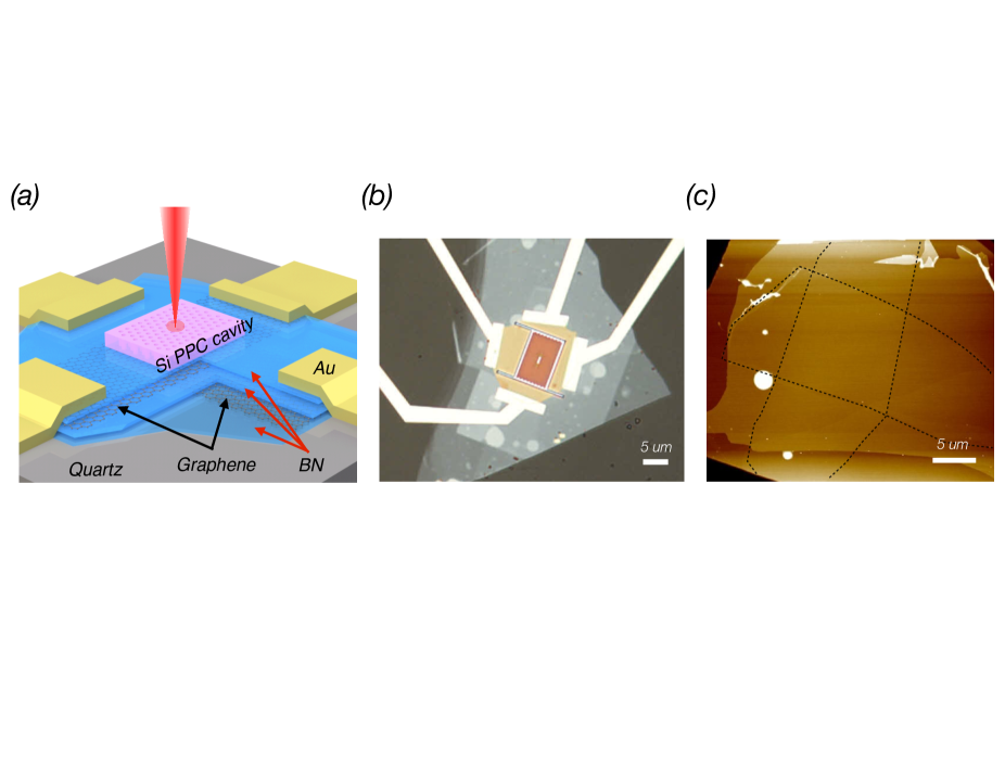
Fig. 1(a) shows the schematic of the cavity-integrated graphene electro-optic modulator. A BN/Graphene/BN/Graphene/BN five-layer stack was built by the van der Waals (vdW) assembly techniqueWang et al. (2013) and then transferred onto a quartz substrate, see Fig. 1(c). Quartz substrates reduce parasitic capacitance compared to more commonly used SiO2/Si substrates. The two graphene sheets were positioned as crossed stripes in order to be contacted individually. The graphene edges were exposed by plasma etchingWang et al. (2013) the five-layer stack using a hydrogen-silsesquioxane (HSQ) resist mask patterned by electron beam lithography (EBL). Metal contacts of Cr/Pd/Au (1/20/50 nm) were deposited by electron beam evaporation, making edge-contact to the two graphene sheets. In this encapsulated dual-layer graphene structure, each one of the graphene sheets can be viewed as a gate and supplys gate voltage to another. The graphene-BN heterostructures made by the vdW technique have demonstrated extremely high room temperature mobility up to 140,000 cm2/Vs, which is comparable to the theoretical acoustic phonon-scattering limitWang et al. (2013).
The PPC cavity was separately fabricated on a silicon-on-insulator (SOI) wafer using a combination of EBL, dry etching, and wet etching. The membrane of the PPC cavity has a thickness of 220 nm and a lattice period of = 420 nm and air hole radius = 0.29 . A linear three-hole (L3) defect defines the cavityAkahane et al. (2003). The PPC lattice was surrounded by a 1-m-wide trench and only connected to the plane of the wafer by four 200-nm-wide bridges, which allowed us to separate them from the parent wafer using an adhesive, transparent Polydimethylsiloxane (PDMS) substrate. Then, using the same vdW technique, we transferred the PPC cavity onto the top surface of the pre-fabricated five-layer-stack device. The PPC cavity was aligned with the overlapping area of the cross-placed two graphene sheets underneath. The completed modulator is shown in Fig. 1(b).
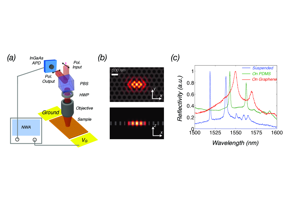
We characterized the PPC cavity using a cross-polarized confocal microscope with a broad-band (super-continuum laser) excitation source, as shown in Fig. 2(a). Before transfer, the suspended cavity membrane exhibited two prominent modes at 1519 nm and 1538 nm with quality factors () of 1500 and 1100, respectively, see blue curve in Fig. 2(c). The polarization of the far-field radiation of the resonance at 1538 nm is orthogonal to the long axis of the L3 cavity, which, together with its energy, indicates the fundamental modeChalcraft et al. (2007). The energy density of this mode, obtained by finite-difference time-domain (FDTD) simulation, is shown in Fig. 2(b). After the cavity was picked up by the PDMS substrate, the cavity resonance red-shifted, and the values dropped to 1050 and 1020, respectively, as seen in the green curve in Fig. 2(c). The red-shift of resonances and decrease of the values are expected due to the increase of the effective cavity mode index and the critical angle for total internal reflection. After the cavity was finally transferred onto the graphene capacitor, shown as red curve in Fig. 2(c), the cavity mode exhibited additional red-shift because of the larger refractive index of quartz () compared to PDMS ( at 1550 nm), and the values sharply descreased to 270 and 250, primarily due to the graphene absorption.
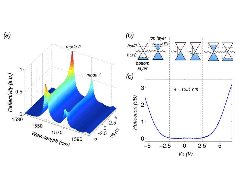
We tested the optical response of the graphene modulator by monitoring the cavity reflection spectrum while slowly sweeping the gate voltage across the top and bottom graphene layer, as shown in Fig. 3(a). When increased from 2.5 V to 6.7 V, the carrier density in the two graphene layers gradually increased, approaching the Fermi energy () of Pauli blocking for an incident photon with angular frequency , as depicted in Fig. 3(b). Therefore, the optical absorption in graphene was reduced, resulting in increased reflection from the cavity and slightly red-shifted peaks. At = 6.7 V, the cavity reflectivity was increased by 2.1 times compared to the near zero-bias regime, i.e., 0 V 2.5 V, corresponding to a maximum modulation depth of 3.2 dB . The spectra for negative bias voltage, -5.6 V 0 V, mimicked the spectra for positive voltage; note that for 0 V, the doping types of top and bottom graphene layers were reversed compared to 0 V. We plot the cavity reflection at nm as a function of in Fig. 3(c). The evolution of the spectrum is symmetric to 0.2 V, indicating low intrinsic doping of the encapsulated dual-layer graphene capacitor.
By fitting the spectrum in Fig. 3(a) to Lorentzian curves, we obtained the variation of values and shift of resonant wavelength as a function of VG. The results are plotted in Fig. S1(a) and Fig. S1(b). The variation of values and shift of resonance wavelength are related to the gate-dependent complex optical conductivity of the graphene sheets. We extracted the real (green) and imaginary (black) components of from the cavity spectra using the perturbation theory modelGan et al. (2012, 2013), as seen in Fig. S1(c) (see supporting information). We notice that the maximum gate voltage applied to the graphene sheets only reduced to half of the value of the undoped graphene, i.e., when . This indicates that the modulation depth could likely be further increased with a larger gate voltage. However, to avoid breakdown ( = 0.3 0.8 V/nmLee et al. (2011); Voskoboynikov et al. (1976)) of the 10 nm central BN layer, we did not push the gate voltage further more. The limitation of the breakdown voltage could be improved by working at longer wavelengths or with high-K materials that provide stronger electric field between two graphene sheets before breakdown.
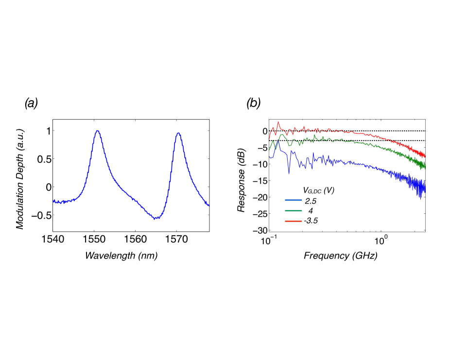
We tested the temporal characteristics by observing the reflected intensity modulation of a narrowband tunable laser (1 MHz spectral bandwidth) coupled into the cavity. The cavity reflection was detected with an InGaAs avalanche photodetector (APD). To address the low coupling efficiency of the probe laser into the cavity, we improved the signal to noise ratio by locking our detection to a 20 kHz amplitude modulation of the probe laser power. To measure the low frequency (3kHz) response, we combined a DC gate voltage of 5.7 V and a sinusoidal signal voltage of = 0.1 V and then applied them across the graphene capacitor. Fig. 4(a) plots the normalized modulation depth for different input laser wavelengths, showing two peaks corresponding to the cavity resonances. For the measurement of high frequency response, we coupled a RF power of -10 dBm with varying DC gate voltages from a 20 GHz network analyzer (NWA) to the dual-layer graphene capacitor. The electrical signal of the InGaAs APD was sent to the input port of the NWA, the measurement result is shown in Fig. 4(b), indicating a high speed response of a low-pass filter characteristic with a 3 dB cut-off frequency of 1.2 GHz. The cut-off frequency is limited by the RC time constant of the dual-layer graphene capacitor, as deduced by the impedance measurement of the device (see supporting information).
In our device, the area of the graphene capacitor is about 100 m2, corresponding to a capacitance of 320 fF. We estimate the switching energy of this device to be approximately 1 pJ (see supporting information). For PPC L3 cavities, the resonant mode area is around 0.5 m2. Therefore, by shrinking the size of the graphene capacitor to only overlap with the mode area, we expect the switching energy to be only 5 fJ and operation spped at 100 GHz (see supporting information). The cavity bandwidth in this work exceeds 600 GHz for a value of 300: i.e., it would be possible to obtain a large modulation contrast without the need of high cavities, as is required in silicon carrier-depletion (injection) modulators. In addition, this broader bandwidth improves temperature stability, which is a limiting factor in the carrier-modulation Si modulatorsManipatruni et al. (2008); Teng et al. (2009); Reed et al. (2010).
In conclusion, we have demonstrated a high-speed, graphene-boron nitride heterostructure based electro-optic modulator integrated with a photonic crystal nanocavity with micrometer scale device footprint. The maximum modulation depth is 3.2 dB with a voltage swing of only 2.5 V. The modulation originates from the variation of optical conductivity of graphene under the effect of different electrostatic potential and the strong coupling between graphene and PPC cavity. At high frequencies, the device exhibits a 3 dB cut-off frequency up to 1.2 GHz. We estimate that by shrinking the device size from 100 m2 to 0.5 m2, the operating speed and switching energy could be improved by two orders of magnitude. These results show that the strong electro-absorptive effect of graphene in a cavity could create efficient optical modulation for on-chip modulators with ultra-low power consumption, ultra-small footprint, high-speed, and relatively broad bandwidth, which make such devices promising for efficient and stable electrical to optical signal conversion in optical communications and signal processing networks.
Acknowledgements.
Financial support was provided by the Office of Naval Research (Award N00014-13-1-0662), Air Force Office of Scientific Research PECASE (supervised by G. Pomrenke), the DARPA Information in a Photon programme (grant no. W911NF-10-1-0416) and by NSF grant DMR-1106225 (T.H.). Device fabrication was partly carried out at the Center for Functional Nanomaterials, Brookhaven National Laboratory, which is supported by the US Department of Energy, Office of Basic Energy Sciences (contract no. DE-AC02- 98CH10886). Device assembly (including graphene transfer) and characterization was supported by the Center for Re-Defining Photovoltaic Efficiency Through Molecule Scale Control, an Energy Frontier Research Center funded by the US Department of Energy, Office of Science, Office of Basic Energy Sciences (award no. DE-SC0001085). R.-J.S. was supported in part by the Center for Excitonics, an Energy Frontier Research Center funded by the US Department of Energy, Office of Science, Office of Basic Energy Sciences under award no. DE-SC0001088.References
- Jalali and Fathpour (2006) B. Jalali and S. Fathpour, Journal of Lightwave Technology 24, 4600 (2006).
- Lee et al. (2010) B. G. Lee, A. Biberman, S. Member, J. Chan, and K. Bergman, 16, 6 (2010).
- Reed et al. (2010) G. T. Reed, G. Mashanovich, F. Y. Gardes, and D. J. Thomson, Nature Photonics 4, 518 (2010).
- Miller (2009) D. A. B. Miller, Proceedings of the IEEE 97, 1166 (2009).
- Liu et al. (2004) A. Liu, R. Jones, L. Liao, D. Samara-Rubio, D. Rubin, O. Cohen, R. Nicolaescu, and M. Paniccia, Nature 427, 615 (2004).
- Xu et al. (2005) Q. Xu, B. Schmidt, S. Pradhan, and M. Lipson, Nature 435, 325 (2005).
- Jacobsen et al. (2006) R. S. Jacobsen, K. N. Andersen, P. I. Borel, J. Fage-Pedersen, L. H. Frandsen, O. Hansen, M. Kristensen, A. V. Lavrinenko, G. Moulin, H. Ou, C. Peucheret, B. Zsigri, and A. Bjarklev, Nature 441, 199 (2006).
- Xu et al. (2007) Q. Xu, S. Manipatruni, B. Schmidt, J. Shakya, and M. Lipson, 15, 430 (2007).
- Alloatti et al. (2011) L. Alloatti, D. Korn, R. Palmer, D. Hillerkuss, J. Li, A. Barklund, R. Dinu, M. Fournier, J. Fedeli, H. Yu, W. Bogaerts, P. Dumon, and R. Baets, 19, 11841 (2011).
- Dong et al. (2012) P. Dong, L. Chen, C. Xie, L. L. Buhl, and Y.-K. Chen, Optics express 20, 21181 (2012).
- (11) G. T. Reed, G. Z. Mashanovich, F. Y. Gardes, M. Nedeljkovic, Y. Hu, D. J. Thomson, K. Li, P. R. Wilson, S.-W. Chen, and S. S. Hsu, Nanophotonics , 1.
- Bonaccorso et al. (2010) F. Bonaccorso, Z. Sun, T. Hasan, and A. C. Ferrari, Nature Photonics 4, 611 (2010).
- Avouris and Freitag (2014) P. Avouris and M. Freitag, IEEE Journal of Selected Topics in Quantum Electronics 20, 6000112 (2014).
- Bao and Loh (2012) Q. Bao and K. P. Loh, ACS nano 6, 3677 (2012).
- Kuzmenko et al. (2008) a. Kuzmenko, E. van Heumen, F. Carbone, and D. van der Marel, Physical Review Letters 100, 117401 (2008).
- Mak et al. (2008) K. F. Mak, M. Y. Sfeir, Y. Wu, C. H. Lui, J. Misewich, and T. F. Heinz, Physical Review Letters 101, 196405 (2008).
- Wang et al. (2008) F. Wang, Y. Zhang, C. Tian, C. Girit, A. Zettl, M. Crommie, and Y. R. Shen, Science (New York, N.Y.) 320, 206 (2008).
- Dean et al. (2010) C. R. Dean, a. F. Young, I. Meric, C. Lee, L. Wang, S. Sorgenfrei, K. Watanabe, T. Taniguchi, P. Kim, K. L. Shepard, and J. Hone, Nature nanotechnology 5, 722 (2010).
- Xia et al. (2009) F. Xia, T. Mueller, Y.-M. Lin, A. Valdes-Garcia, and P. Avouris, Nature nanotechnology 4, 839 (2009).
- Liu et al. (2011) M. Liu, X. Yin, E. Ulin-Avila, B. Geng, T. Zentgraf, L. Ju, F. Wang, and X. Zhang, Nature 474, 64 (2011).
- Liu et al. (2012) M. Liu, X. Yin, and X. Zhang, Nano letters 12, 1482 (2012).
- Gan et al. (2013) X. Gan, R.-J. Shiue, Y. Gao, K. F. Mak, X. Yao, L. Li, A. Szep, D. Walker, J. Hone, T. F. Heinz, and D. Englund, Nano letters 13, 691 (2013).
- Majumdar et al. (2012) A. Majumdar, J. Kim, J. Vuckovic, and F. Wang, arXiv 1210.6716, 1 (2012).
- Li et al. (2008) Z. Q. Li, E. a. Henriksen, Z. Jiang, Z. Hao, M. C. Martin, P. Kim, H. L. Stormer, and D. N. Basov, Nature Physics 4, 532 (2008).
- Gan et al. (2012) X. Gan, K. F. Mak, Y. Gao, Y. You, F. Hatami, J. Hone, T. F. Heinz, and D. Englund, Nano letters 12, 5626 (2012).
- Wang et al. (2013) L. Wang, I. Meric, P. Y. Huang, Q. Gao, Y. Gao, H. Tran, T. Taniguchi, K. Watanabe, L. M. Campos, D. a. Muller, J. Guo, P. Kim, J. Hone, K. L. Shepard, and C. R. Dean, Science (New York, N.Y.) 342, 614 (2013).
- Akahane et al. (2003) Y. Akahane, T. Asano, and B.-s. Song, 425, 4 (2003).
- Chalcraft et al. (2007) A. R. A. Chalcraft, S. Lam, D. O’Brien, T. F. Krauss, M. Sahin, D. Szymanski, D. Sanvitto, R. Oulton, M. S. Skolnick, A. M. Fox, D. M. Whittaker, H.-Y. Liu, and M. Hopkinson, Applied Physics Letters 90, 241117 (2007).
- Lee et al. (2011) G.-H. Lee, Y.-J. Yu, C. Lee, C. Dean, K. L. Shepard, P. Kim, and J. Hone, Applied Physics Letters 99, 243114 (2011).
- Voskoboynikov et al. (1976) V. V. Voskoboynikov, V. A. Gritsenko, V. M. Efimov, V. E. Lesnikovskaya, and F. L. Edelman, Physica Status Solidi (a) 34, 85 (1976).
- Manipatruni et al. (2008) S. Manipatruni, R. K. Dokania, B. Schmidt, N. Sherwood-Droz, C. B. Poitras, A. B. Apsel, and M. Lipson, Optics letters 33, 2185 (2008).
- Teng et al. (2009) J. Teng, P. Dumon, W. Bogaerts, H. Zhang, X. Jian, X. Han, M. Zhao, G. Morthier, and R. Baets, Optics express 17, 14627 (2009).