Accumulation, inversion, and depletion layers in SrTiO3
Abstract
We study potential and electron density depth profiles in accumulation, inversion and depletion layers in crystals with a large and nonlinear dielectric response such as . We describe the lattice dielectric response using the Landau-Ginzburg free energy expansion. In accumulation and inversion layers we arrive at new nonlinear dependencies of the width of the electron gas on an applied electric field . Particularly important is the predicted electron density profile of accumulation layers (including the interface) , where . We compare this profile with available data and find satisfactory agreement. For a depletion layer we find an unconventional nonlinear dependence of the capacitance on voltage. We also evaluate the role of spatial dispersion in the dielectric response by adding a gradient term to the Landau-Ginzburg free energy.
pacs:
73.20.-r,71.10.Ca,73.30.+y,68.47.GhI Introduction
In recent years, there has been growing interest in the investigation of perovskite crystals, which are important for numerous technological applications and show intriguing magnetic, superconducting, and multiferroic properties Chakhalian et al. (2014). Special attention Stemmer and Allen (2014); Zubko et al. (2011) is paid to heterostructures involving which is a semiconductor with a band gap of Noland (1954) and a large dielectric constant ranging from at liquid helium temperatures to at room temperature. As with conventional semiconductors, can be used as a building block for different types of devices, with reasonably large mobility Ohtomo and Hwang (2004); Xie et al. (2013).
Many devices are based on the accumulation layer of electrons near a heterojunction interface involving . For example, one can use modulation doping in the structure / to introduce electrons in the conduction band of from donors within the wider-band-gap material Kajdos et al. (2013). Inside bulk -doping can be used to introduce two accumulation layers of electrons Jalan et al. (2010); Kozuka et al. (2010); Kaiser et al. (2012). One can accumulate an electron gas using a field-effect Thiel et al. (2006); Hosoda et al. (2013); Boucherit et al. (2014) instead of dopants. In Refs. Ueno et al., 2008; Gallagher et al., 2014 the authors accumulated up to electrons on the surface of using ionic liquid gating. Finally, there is enormous interest Ohtomo and Hwang (2004); Xie et al. (2013); Stemmer and Allen (2014) in heterojunctions where electrons are accumulated by the electric field resulting from the “polar catastrophe” Nakagawa et al. (2006). It is natural to think that the depth profiles of the potential and electron density inside have a universal origin in all these devices.
Another type of device based on -doped is the Schottky diode. Due to the built-in Schottky barrier the region near the metal-semiconductor interface in doped is depleted. The large and nonlinear dielectric constant results in unconventional capacitance-voltage characteristics. Schottky diodes with different metals and bulk dopants have been studied: Hikita et al. (2011), Yamamoto et al. (1997), Hikita et al. (2007), and Verma et al. (2014).
All of the devices cited above are based on accumulation and depletion layers. We do not know of any attempts to create a hole inversion layer in -type or an electron inversion layer in -type but they are likely to be of interest as well.
Interface properties determine characteristics of all these devices. Not surprisingly, the potential and electron density depth profiles in such devices have attracted attention from the experimental Minohara et al. (2014); Yamada et al. (2014); Dubroka et al. (2010); Moetakef et al. (2011) and theoretical points of view Khalsa and MacDonald (2012); Ueno et al. (2008); Stengel (2011); Son et al. (2009); Park and Millis (2013); Haraldsen et al. (2012). For example, experimental data show that electrons are distributed in a layer of width near the interface. Theoretical works that attempt to explain such behavior are based on microscopic numerical calculations.
The goal of this paper is to create a simple, mostly phenomenological and analytical approach for describing the potential and the electron density depth profiles in . To account for the nonlinear dielectric response in we use the Landau-Ginzburg free energy expansion Ginzburg (1946); Landau and Lifshitz (1980). Electrons are almost everywhere described in the Thomas-Fermi approximation Thomas (1927). Although we mostly concentrate on , the developed approach is applicable to Rowley et al. (2014) and Kim et al. (1992) as well.
Our main result is a new form for the potential and electron density depth profiles in accumulation, inversion and depletion layers due to the nonlinear dielectric response. In particular, for an accumulation layer in , we find an electron concentration that depends on the distance from the surface as , where the width decreases with the external electric field as . These relations seem to agree with experimental data Dubroka et al. (2010); Yamada et al. (2014).
The remainder of this paper is organized as follows. In Sec. II we define the model based on the Landau-Ginzburg theory for calculating the lattice dielectric response and describe the parameters of . In Sec. III we use the Thomas-Fermi approach for calculating the self-consistent electric field to describe properties of electron accumulation layers. In the Sec. IV we apply our theory to the consideration of interfaces between and polar dielectrics. In particular, we pay attention to the case of an accumulation layer on the interface of and compare our theory with experimental data. In Sec. V we calculate the quantum capacitance of the accumulation layer in . In Sec. VI we use a one sub-band approximation, in which electrons do not affect the electric field, to calculate properties of inversion layers. In Sec. VII we consider a depletion layer in , calculate the capacitance-voltage characteristics of a Schottky barrier for such systems, and compare our results with experimental data. In Sec. VIII we show that our results are not modified by the presence of spatial dispersion in the dielectric response. Sec. IX provides a summary and conclusion.
II The model
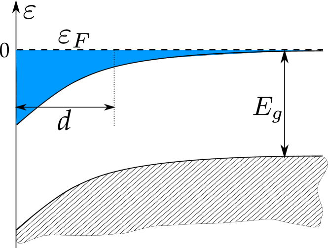
Bulk typically is an -type semiconductor with a concentration of donors . Let us discuss the position of Fermi energy in such crystals. The electron spectrum near the bottom of the conduction band is complicated van der Marel et al. (2011), and in order to make the problem of an accumulation layer tractable analytically we assume that it is isotropic and non-degenerate with the effective mass , Ahrens et al. (2007) where is free electron mass. Within the hydrogenic theory of shallow donors, the donor Bohr radius is equal to , where , is the electron charge, and is dielectric constant of the material. At room temperature when , the Bohr radius is so large that the Mott criterion for the metal-insulator transition in doped semiconductors leads to a very small critical concentration . At helium temperatures and . Thus, at the experimentally relevant concentration of donors , we are dealing with a heavily doped semiconductor in which the Fermi energy lies in the conduction band of . On the other hand, due to the relatively high effective mass the bulk Fermi energy is smaller than the bending energy of the conduction band bottom near the interface (see Figs. 1 and 6). For example, for , the Fermi energy calculated from the bottom of the conduction band is which can be up to times smaller than the bending energy of the conduction band bottom in an accumulation layer for . Therefore, we assume below that the Fermi energy coincides with the bottom of the conduction band.
We are interested in accumulation, inversion and depletion layers near an interface of . We consider the case when the axis is directed perpendicular to the interface (plane ) and lies along the [100] axis of a cubic crystal of . (In fact, changes symmetry from cubic to tetragonal at , but the distortion is small Lytle (1964) and can be neglected). An external electric field applied from the left (see Figs. 1, 4, 6) is directed along the axis. In that case the problem is effectively one-dimensional. If the charge density is denoted by , then the potential depth profile in the system is determined by the equations:
| (1) |
where are electric induction, electric field and polarization in . Equations (1) should be solved with proper boundary conditions. For example, for an accumulation layer the boundary conditions are and .
To solve the system (1) one needs to know two material relationships and . Let us start from the lattice dielectric response . is well known as a quantum paraelectric, where the onset of ferroelectric order is suppressed by quantum fluctuations Itoh et al. (1999).
A powerful approach to describe the properties of ferroelectric-like materials is based on the Landau-Ginzburg theory. For a continuous second-order phase transition the Landau-Ginzburg expression of the free energy density is represented as a power series expansion with respect to the polarization :
| (2) |
where stands for the free energy density at and is the inverse susceptibility . In this work , is the characteristic polarization and Lytle (1964) is the lattice constant. The coefficient A describes the non-linear dielectric response. Analyzing the available data van der Berg et al. (1995); Yamamoto et al. (1997, 1998); Mikheev et al. (2014) in Section VII we find values of between 0.5 and 1.5. For all estimates below we use following from Ref. Mikheev et al. (2014). The last term of Eq. (2) is responsible for the interaction between the polarization and the electric field . In general depends on the components of the vector , but in the chosen geometry the problem is one-dimensional, and all vectors are directed along the axis. The crystal polarization is determined by minimizing the free energy density in the presence of the electric field , . This condition relates and ,
| (3) |
We note that and thus . The electric field at which the transition from linear to nonlinear dielectric response occurs can be found by equating the first and second terms in the expression (3):
| (4) |
If the dielectric response of is linear and one can use the simplified expression for the electric field:
| (5) |
For the dielectric response of is nonlinear and one must instead use the expression:
| (6) |
Next one should specify , which depends on the specific device of interest.
III Accumulation layer: Theory
In an accumulation layer the external electric field attracts electrons with a three-dimensional concentration (see Fig. 1). Our goal is to find the electron depth profile and its characteristic width .
Due to electric neutrality the number of accumulated electrons has to compensate the external field , i.e.,
| (7) |
To take into account the electron screening of the external field we use the Thomas-Fermi approach Thomas (1927) in which the electron concentration and self-consistent potential profile are related as , where
| (8) |
is the chemical potential of the electron gas. Thus, one can obtain the solution of Eqs. (1) by replacing with and using relations (5) and (6). For a linear dielectric response we obtain the equation for the potential:
| (9) |
We use the boundary condition at and get the solution:
| (10) |
| (11) |
where and . ( was derived equivalently in Ref. Stratton, 1955 as a work function reduction for .) For a nonlinear dielectric response we obtain the equation for the potential:
| (12) |
With the same boundary condition we get the solution:
| (13) |
| (14) |
where
The characteristic length can be obtained using the neutrality condition (see Eq. (7)). For a linear dielectric response this gives:
| (15) |
where . For a nonlinear dielectric response:
| (16) |
where . The electric field at which the transition from linear to nonlinear dielectric response occurs can be found from equating Eqs. (15) and (16). This gives
| (17) |
where , consistent with Eq. (4). For , the critical field depends on temperature: for helium temperature and for room temperature.
The three dimensional concentration profile for the nonlinear dielectric response Eq. (14) is the main result of our paper. Note that has a very long tail with a weak power law dependence, which may lead to some arbitrariness in measurements of the width of the electron gas. Indeed, only 39% of electrons are located within the distance near the interface and 68% of electrons are located within . In the calculation above we used a space-continuous model. Actually, along the [100] axis is composed of alternating and layers. The conduction band of corresponds to the bands composed of mainly orbitals of . Integrating over each lattice cell in Table (1) we get a percentage of electrons in each of the 10 first layers of for the case .
| M | 1 | 2 | 3 | 4 | 5 | 6 | 7 | 8 | 9 | 10 |
|---|---|---|---|---|---|---|---|---|---|---|
| Percent | 27.9 | 14.4 | 9.0 | 6.2 | 4.6 | 3.5 | 2.8 | 2.3 | 1.9 | 1.6 |
One can see from Eqs. (11) and (14) that the tails of the electron depth profiles at do not depend on and behave like
and
for linear and nonlinear dielectric responses, respectively. Even for , when the electron distribution at moderately large is described by dependence (14), at very large distances the polarization becomes smaller and the linear dielectric response takes over so that the dependence switches from Eq. (14) to Eq. (11). This happens at the distance
( and for helium and room temperature respectively). Thus, the tail of is universal. For small the tail has the form . For it has the form for and for .
On the other hand, one has to remember that our theory is correct only when is larger than the concentration of donors in the bulk of the material.
Let us verify whether the Thomas-Fermi approximation is applicable, i.e., . Here is the wavevector of an electron at the Fermi level. For
| (18) |
while for
| (19) |
where , One can see that in the range of for room temperature. For lower temperatures this interval is even larger. Thus, the Thomas-Fermi approximation is applicable for practically all reasonable electric fields . 111So far we considered only two limiting cases: the linear and nonlinear dielectric responses, which are correct for and respectively. In fact one can analytically solve Eqs. (1) with Eq. (3) assuming that . For example, in Ref. Gureev et al., 2011 the polarization profile of a charged “head-to-head” domain wall in a ferroelectric was calculated. In the ferroelectric phase, the spontaneous polarization in the domain is approximately equal to our . Therefore a charged domain wall, considered in Ref. Gureev et al., 2011, should be compared with our accumulation layer at the crossover value of the electric field, . Indeed, our results Eqs. (11), (15) taken at agree with those for the charged domain wall.
IV Accumulation layer: Comparison with experimental data
It is widely believed that an electron gas emerges near polar/non-polar interfaces such as Moetakef et al. (2011); Boucherit et al. (2014), He et al. (2012), , , Annadi et al. (2012), Perna et al. (2010) and Ohtsuka et al. (2010) due to the polar catastrophe Nakagawa et al. (2006). For a large enough thickness of the polar crystal Son et al. (2009) the interface electron surface charge density
| (20) |
is equal to , which corresponds to [see Eq. (7)]. For any temperature this field is much larger then the critical field and Eq. (19) gives . Thus, we arrive at Eq. (14) for the electron concentration and Eq. (16) shows that . In this case 68% of electrons are located within . This result agrees with experimental estimates of the width of an electron gas near the interface Moetakef et al. (2011). It also agrees with experimental data Chen et al. (2013) for the interface where a 2DEG is formed due to the formation of oxygen vacancies on . In the case of -doped with one layer of La Ohtomo et al. (2002) one has two accumulation layers each with and a similar width .
To see how important the nonlinear dielectric response is, one can compare its prediction to the one obtained by assuming the response to be linear, given by Eq. (15). For and helium temperature the linear dielectric response gives . A similar result was obtained in Ref. Siemons et al., 2007, where the nonlinear dielectric response was not taken into account.
For the interface the number of electrons accumulated is apparently smaller than what the “polar catastrophe” scenario predicts. For example, only of the electrons are seen in Hall measurements Thiel et al. (2006); Caviglia et al. (2008); Mathew et al. (2013). In order to describe the electron concentration for such a surface charge density, , one can still use Eq. (14) and Eq. (16). As a result, we arrive at a much larger value of .
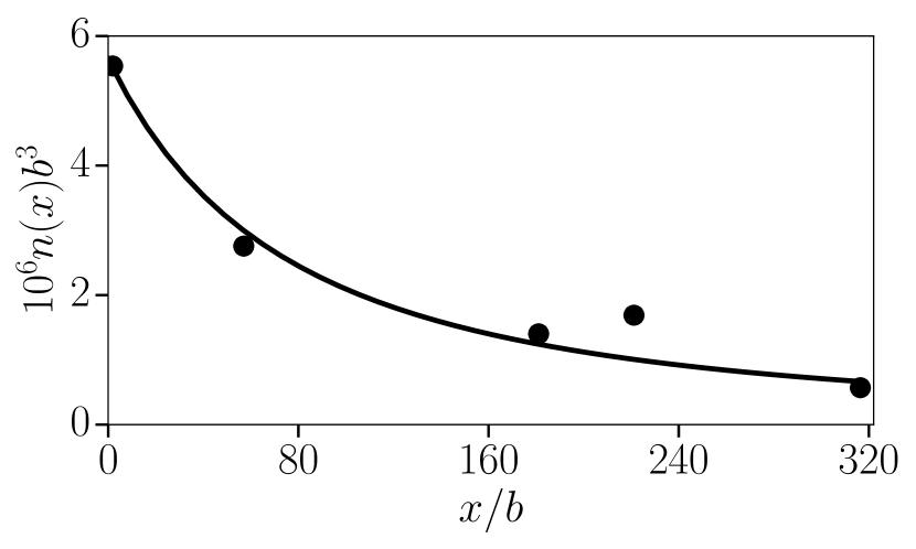
We test our theory for the functional shape of by comparing to experimental data for the electron distribution near the interface of at temperature Dubroka et al. (2010) (see Fig. 2). For such small temperatures the critical field is small and we fit the experimental data by Eq. (14) with as a fitting parameter and get with . Figure 2 shows satisfactory agreement between the data and the shape of described by Eq. (14).
Let us now dwell upon the experimental data for from Ref. Yamada et al., 2014. The data are obtained via time-resolved photoluminescence spectroscopy of the interface, where interface-induced electrons radiatively recombine with photoexcited holes in . Following the assumption from Ref. Yamada et al., 2014 that the photoexcited holes are immobile, the concentration of holes decays with time according to the equation:
| (21) |
where is the hole trapping rate and is the three carrier non-radiative Auger recombination coefficient. The authors of Ref. Yamada et al., 2014 used the decay of the photoluminescence intensity to obtain in with the help of the coefficients from Ref. Yamada et al., 2009. The resulting is shown in Fig. 3 by filled circles. We fit this data by the equation
| (22) |
which is similar to Eq. (14), but is a fitting parameter independent of . We see from Fig. 3 that this fit is good, however, the parameter is seven times larger than the parameter entering Eq. (14). This can be explained by a 50-fold increase of the Auger coefficient of Eq. (21) near the interface. A similar surface effect was observed in Ref. Yamada et al., 2011 for nanocrystals, where is almost 150 times larger than for bulk .
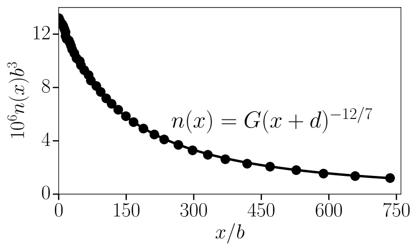
From the fit we get , which corresponds to an electron surface charge density in agreement with other data Thiel et al. (2006); Caviglia et al. (2008); Dubroka et al. (2010). One can check that this result is self-consistent, i.e. for such one can use Eq. (14) for the fitting of experimental data, because (see Eq. (19)) and (see Eq. (17)).
V Quantum capacitance of an accumulation layer
In this section we address the capacitance of an accumulation layer, for example in the double junction . If the width of insulating layer we may view an accumulation layer as a conducting two-dimensional gas (2DEG). One can apply a positive voltage between the metal and the 2DEG and measure the additional charge per unit area and , which are induced on the metal and in the 2DEG, respectively. The capacitance per unit area of junction is . If we imagine that the 2DEG is a perfect metal, the additional charge resides exactly in the plane of the junction and the capacitance is equal to the geometric capacitance , where is the dielectric constant of the layer. Actually, the accumulation layer is not a perfect metal so that an additional negative charge is distributed in a layer of finite width . As a result , where is called the quantum capacitance Luryi (1988). Quantum capacitance is broadly studied for many 2DEGs such as silicon MOSFETs Kravchenko et al. (1990), hetero-structures Eisenstein et al. (1992) and graphene Ponomarenko et al. (2010).
Concentrating on the case of and using Eqs. (12) and (16) for the potential difference between and we have at :
| (23) |
After the transfer of charge from the metal to the electron gas the potential changes as:
| (24) |
Assuming that , linearizing with respect of and adding the voltage drop across the layer we get
Using Eq. (16) for we can write for the total capacitance:
| (25) |
where
is the effective nonlinear dielectric constant at (see Eq. (6)) . The first term of Eq. (25) is the inverse quantum capacitance , and the last term is the inverse geometric capacitance .
Due to the polar catastrophe in we get and . The ratio of inverse capacitances is
For we get . One can extend our calculation to the double junction . In that case the inverse quantum capacitance is the sum of inverse quantum capacitances of both junctions.
VI From accumulation to inversion layer
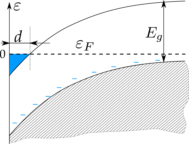
In the previous section we considered an accumulation layer and showed that it can be described by the Thomas-Fermi approximation, when the Fermi level is near the bottom of the conduction band. But the Fermi level can be moved into the gap, for example, by a back gate. In a -type inversion layer in (see Fig. 4) the Fermi level can be even deeper, at the top of the bulk valence band. In both cases, the charge of electrons compensates only a fraction of the external electric field , i. e., Eq. (7) is violated. For example, the rest of the negative charge in the inversion layer is provided by negative acceptors [see Fig. 4] and the electron surface charge density . To calculate the width of the electron density profile below we use a scaling approach, i.e. we neglect all numerical coefficients.
If the surface electron density is high enough , the electron gas is three-dimensional (3DEG), and one can use the Thomas-Fermi approach and the kinetic energy is
[see Fig. 5(a)]. On the other hand at , the electrons are confined to the first sub-band of the triangular potential well, so that the electron gas is two dimensional (2DEG) Ando et al. (1982). The electron kinetic energy is then
In both cases, the characteristic potential energy of electrons is [see Fig.5(b)].
The dielectric response can be linear or nonlinear depending on whether the external electric field is smaller or larger than , respectively. This gives us four cases which correspond to high and low electron charge density, small field, , and large field, . The diagram in Fig. 5 (c) shows the combined scaling results for for all these four domains. We use as an independent coordinate because the three-dimensional concentration can be obtained by Hall effect measurements, while can also be measured independently Yamada et al. (2014).
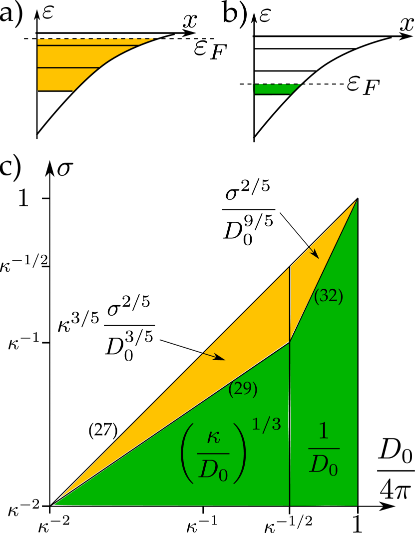
First, let us consider the domain of high electron charge density and small field . The kinetic energy is and the potential energy is . From the condition one obtains:
| (26) |
[see Fig. 5(c)]. When the neutrality relation (7) is satisfied
| (27) |
we recover the previous accumulation layer result, Eq. (15). For low electron charge density and small field we get
| (28) |
This is the classical result for the width of the inversion layer Stern (1972). The critical electron density at which the transition from low to high electron charge density occurs can be obtained from the condition or from equating expressions (26) and (28) for , giving
| (29) |
We emphasize the difference between the two regimes of low [Eq. (28)] and high [Eq. (26)] electron charge densities. Sometimes Khalsa and MacDonald (2012); Ueno et al. (2008), Eq. (28) for of an inversion layer is used for an accumulation layer.
So far we described the two left, low () domains of Fig. 5c. For a large field and a high electron charge density we get
| (30) |
At , i.e. when the neutrality relation is satisfied, we get the previous result Eq. (16). At last, for a low electron charge density and large field we get
| (31) |
The transition from low to high electron charge density at occurs at the critical electron density:
| (32) |
All four results Eqs. (26), (28), (30), (31) and all the border lines between different domains, Eqs. (27), (29), (32), are shown in Fig. 5c.
VII Depletion layer
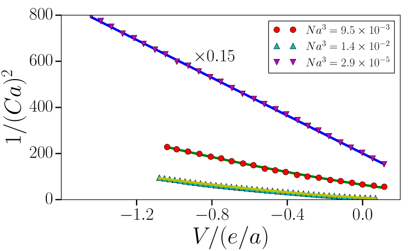
Schottky diodes are metal--type- junctions where the electron gas is depleted near the interface. Below we calculate the capacitance of this junction as a function of concentration of donors and applied voltage , which has been experimentally studied Hikita et al. (2011, 2007); Verma et al. (2014); Yamamoto et al. (1997).
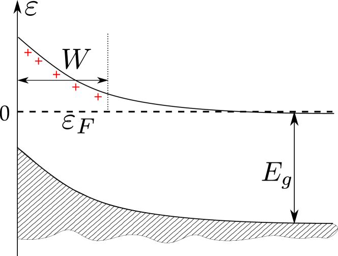
In order to calculate the capacitance of the Schottky diode let us consider Eqs. (1). We use the full depletion approximation, in which we assume that is fully depleted from electrons over a distance from the surface (Fig. 6). The charge density in that region is due to the ionized donors with 3D concentration :
| (33) | |||||
From equations (33) and (1), one can determine the dependence of the width on the potential drop across the depletion layer , where the negative voltage is applied to the metal and is the potential difference between the work functions of and the metal. If one can use the linear relation (5) to get:
| (34) |
If , we use the nonlinear expression (6):
| (35) |
Now one can calculate the capacitance per unit area of the Schottky diode
This gives
| (36) |
for , and
| (37) |
for . With growing the cross-over between Eqs. (36) and (37) happens at where:
| (38) |
To test our theoretical predictions we consider the experimental data obtained at room temperature for lightly and heavier -doped of Ref. Yamamoto et al. (1997), and as well as the more heavily doped sample of Ref. Mikheev et al., 2014 (see Fig. 7). In the first case, one can expect to be small and we use Eq. (36) to fit the experimental data. Using and as fitting parameters we get , , which is close to the room temperature value for . For the heavier doped samples, one can expect that is large and use Eq. (37) to find and from the experimental data. As a result, we get , and , for the data of Refs. Yamamoto et al., 1997 and Mikheev et al., 2014, respectively. 222One can verify whether Eqs. (36) and (37) are applicable for describing the capacitance-voltage characteristics. To do this we consider the critical voltage (38). For small concentration is smaller than the experimental voltage (see Fig. 7). It means that using Eq. (36) is justified. For high concentrations or is larger than the experimental voltage . For such voltages one can use Eq. (37).
In Refs. van der Berg et al., 1995; Yamamoto et al., 1997, 1998; Mikheev et al., 2014; Kahng and Wemple, 1965 data are used to derive , which agrees with the Landau description Yamamoto et al. (1998). Extracting the parameter from of Ref. van der Berg et al., 1995 gives , while in Refs. Yamamoto et al., 1997; Mikheev et al., 2014 lead to the above mentioned values of . The scatter of values of probably can be explained by the effect of a non-controllable “dead layer” of low dielectric constant between and the metal Yamamoto et al. (1997); Mikheev et al. (2014).
It is believed Mikheev et al. (2014) the best interface was made in Ref. Mikheev et al., 2014, whose data lead to . Above we used this value for all numerical estimates. 333Note that there are several other methods Neville et al. (1972); Fleury and Worlock (1968) to study the non-linear dielectric response, but they deal with relatively weak electric fields, while we are interested in strong electric fields.
VIII Does spatial dispersion of dielectric response affect the accumulation layer?
So far we assumed that the external field and polarization change abruptly at the interface, i.e., we have ignored the dispersion of the dielectric response. In this section we show that even without this assumption, the results of previous sections remain intact for . We concentrate on an accumulation layer which can be so narrow that the question of spatial dispersion arises. To take into account that the electric field and polarization can not change abruptly, in the geometry chosen above we add the gradient term to the Landau-Ginzburg free energy density Eq. (2). Here in the general expression for the gradient term
and enumerate the three coordinates . Adding such a term necessitates an additional boundary condition for at . The general form of this condition Kretschmer and Binder (1979) is . It does not bring new physics into the problem if is large. Therefore, we explore the opposite case where can be ignored, . From the condition we get:
| (39) |
Let us first find a solution to Eqs. (1) together with Eq. (39) for a system without electrons (). The electrical induction is constant everywhere and we get an approximate solution for :
| (40) |
where is the electric field in the bulk.
Now, we take electrons into account and start from the case where in Eq. (39) and , so that the role of the gradient term is emphasized. From the resulting equation we get . (We take into account that at , .) From the condition we get an equation for the potential:
| (41) |
(compare with Eq. (9)). The solution to this equation, with boundary condition is:
| (42) |
where and is still an unknown length, which can be found from the boundary condition. Let us describe this solution. First, we see that the solution critically depends on the parameter . If or then one arrives at Eq. (40): the electric field and potential decay exponentially to zero as .
Let us consider the case when or . In that case we get a result similar to Eq. (10), but with
| (43) |
Thus, at the electrons screen the external field much faster than the lattice, and hence the latter does not participate appreciably in the screening response.
One can try to estimate assuming that the majority of electrons are in the region . In that case the potential is given by Eq. (43) and can be found from the condition of neutrality (7):
| (44) |
The condition required for applicability of Eq. (43), is valid only when , where
| (45) |
Let us now consider the opposite case , where most of the electrons are not located in the region . In fact, to find where they are located one has to introduce finite and . The exponential decay of the electric field with saturates at the level of . At larger we reach the electron gas with a larger width given by Eqs. (15) or (16) for linear and nonlinear dielectric responses respectively. In this case, the electron gas resides at large distances and our considerations of the previous section are valid.
If we return to finite and in Eq. (39) in the first case , we arrive to following hybrid picture. An electron gas screens most of the external field at small . At larger distances we again get exponential decay described by Eq. (40), which results from the lattice response. After this exponential decay the electron concentration again follows Eq. (11) or Eq. (14), with the bulk value of the dielectric constant . In other words, the electron density has a two component distribution. The electrons nearest to the interface are likely localized due to disorder. This could, in principle, create hope to explain why at the interface only 10% of the electrons predicted by the polar catastrophe, , are observed in transport measurements.
However, this hope does not survive for actual parameters of , Tagantsev and Gerra (2006) . Although for such parameters the Thomas-Fermi approximation is still valid, the electric field at which all electrons are located within the distance from the interface, is so large that always. One may also worry that for such values of and , which are smaller than the lattice constant of , the continuous theory that we use is not applicable.
However, the applicability of the continuous theory can be much better due to the so called background dielectric constant Tagantsev and Gerra (2006). Indeed, until now we have described the entire dielectric response by the Landau-Ginzburg theory for a single order parameter, which can be identified with the displacement of the transversal optical soft mode of This is a good approach when the dielectric response is very strong. However, near the interface the response of the soft mode is weakened due to the dispersion and the response of other optical modes as well as the polarization of ions must be included. This is done Tagantsev and Gerra (2006) by the addition of the linear non-dispersive background dielectric constant, Tagantsev and Gerra (2006); Shannon (1993). To model this situation one can replace by the soft mode contribution in the free energy density (2) and add to it while keeping in Eqs. (1). Here is the background polarization.
As a result, the small distance dielectric constant becomes instead of 1 and the lengths , and the characteristic field of Eq. (45) are replaced by , and , respectively. For the characteristic lengths and may reach the lattice constant , thereby improving the applicability of our theory. At the same time the critical field becomes even larger so that in all realistic situations, , all electrons are located at distances larger than the lattice constant . This means that the dispersion does not play a substantial role and the dispersion-less approach used in the previous sections is applicable for describing accumulation, inversion and depletion layers in .
IX Conclusion
In this paper we studied the potential and electron density depth profiles in accumulation, inversion and depletion layers for materials with a very large dielectric constant and nonlinear dielectric response such as . In particular, we showed that in a depletion layer at a given donor concentration and for high enough voltage, the dependence of the capacitance on voltage decreases as , which is substantially different from the conventional result with linear dielectric response. For an inversion layer we found that the layer width depends on the external electric field as and for linear and nonlinear dielectric responses, respectively. In accumulation layers near interfaces like , , and we obtained with , due to the nonlinearity of the dielectric response. We found that 70% of electrons are located within of the interfaces and (where the electron surface charge density is ) in agreement with experimental data. The predicted functional shape of the electron depth profile also shows satisfactory agreement with the experimental data. Spatial dispersion in the dielectric response was shown to be negligible for the description of potential and electron density depth profiles in devices. This paper uses a simplified isotropic electron spectrum, while the electronic structure of is multiorbital in nature. In future work we plan to go beyond our simplified description.
Acknowledgements.
We are grateful to A. P. Levanyuk and S. Stemmer for reading the manuscript and attracting our attention to a number of important references. We thank R. M. Fernandes, B. Jalan, A. Kamenev, B. Skinner, C. Leighton, A. J. Millis, A. Sirenko and P. Wölfle for helpful discussions. This work was supported primarily by the National Science Foundation through the University of Minnesota MRSEC under Award Number DMR-1420013.References
- Chakhalian et al. (2014) J. Chakhalian, J. W. Freeland, A. J. Millis, C. Panagopoulos, and J. M. Rondinelli, Rev. Mod. Phys. 86, 1189 (2014).
- Stemmer and Allen (2014) S. Stemmer and S. J. Allen, Annual Review of Materials Research 44, 151 (2014).
- Zubko et al. (2011) P. Zubko, S. Gariglio, M. Gabay, P. Ghosez, and J.-M. Triscone, Annual Review of Condensed Matter Physics 2, 141 (2011).
- Noland (1954) J. A. Noland, Phys. Rev. 94, 724 (1954).
- Ohtomo and Hwang (2004) A. Ohtomo and H. Y. Hwang, Nature 427, 423 (2004).
- Xie et al. (2013) Y. Xie, C. Bell, Y. Hikita, S. Harashima, and H. Y. Hwang, Advanced Materials 25, 4735 (2013).
- Kajdos et al. (2013) A. P. Kajdos, D. G. Ouellette, T. A. Cain, and S. Stemmer, Applied Physics Letters 103, 082120 (2013).
- Jalan et al. (2010) B. Jalan, S. Stemmer, S. Mack, and S. J. Allen, Phys. Rev. B 82, 081103 (2010).
- Kozuka et al. (2010) Y. Kozuka, M. Kim, H. Ohta, Y. Hikita, C. Bell, and H. Y. Hwang, Applied Physics Letters 97, 222115 (2010).
- Kaiser et al. (2012) A. M. Kaiser, A. X. Gray, G. Conti, B. Jalan, A. P. Kajdos, A. Gloskovskii, S. Ueda, Y. Yamashita, K. Kobayashi, W. Drube, S. Stemmer, and C. S. Fadley, Applied Physics Letters 100, 261603 (2012).
- Thiel et al. (2006) S. Thiel, G. Hammerl, A. Schmehl, C. W. Schneider, and J. Mannhart, Science 313, 1942 (2006).
- Hosoda et al. (2013) M. Hosoda, C. Bell, Y. Hikita, and H. Y. Hwang, Applied Physics Letters 102, 091601 (2013).
- Boucherit et al. (2014) M. Boucherit, O. Shoron, C. A. Jackson, T. A. Cain, M. L. C. Buffon, C. Polchinski, S. Stemmer, and S. Rajan, Applied Physics Letters 104, 182904 (2014).
- Ueno et al. (2008) K. Ueno, S. Nakamura, H. Shimotani, A. Ohtomo, N. Kimura, T. Nojima, H. Aoki, Y. Iwasa, and M. Kawasaki, Nat Mater 7, 855 (2008).
- Gallagher et al. (2014) P. Gallagher, M. Lee, J. R. Williams, and D. Goldhaber-Gordon, Nature Physics 10, 748 (2014).
- Nakagawa et al. (2006) N. Nakagawa, H. Y. Hwang, and D. A. Muller, Nature Materials 5, 204 (2006).
- Hikita et al. (2011) Y. Hikita, M. Kawamura, C. Bell, and H. Y. Hwang, Applied Physics Letters 98, 192103 (2011).
- Yamamoto et al. (1997) T. Yamamoto, S. Suzuki, H. Suzuki, K. Kawaguchi, K. Takahashi, and Y. Yoshisato, Japanese Journal of Applied Physics 36, L390 (1997).
- Hikita et al. (2007) Y. Hikita, Y. Kozuka, T. Susaki, H. Takagi, and H. Y. Hwang, Applied Physics Letters 90, 143507 (2007).
- Verma et al. (2014) A. Verma, S. Raghavan, S. Stemmer, and D. Jena, Applied Physics Letters 105, 113512 (2014).
- Minohara et al. (2014) M. Minohara, Y. Hikita, C. Bell, H. Inoue, M. Hosoda, H. K. Sato, H. Kumigashira, M. Oshima, E. Ikenaga, and H. Y. Hwang, arXiv:1403.5594 (2014).
- Yamada et al. (2014) Y. Yamada, H. K. Sato, Y. Hikita, H. Y. Hwang, and Y. Kanemitsu, Applied Physics Letters 104, 151907 (2014).
- Dubroka et al. (2010) A. Dubroka, M. Rössle, K. W. Kim, V. K. Malik, L. Schultz, S. Thiel, C. W. Schneider, J. Mannhart, G. Herranz, O. Copie, M. Bibes, A. Barthélémy, and C. Bernhard, Phys. Rev. Lett. 104, 156807 (2010).
- Moetakef et al. (2011) P. Moetakef, T. A. Cain, D. G. Ouellette, J. Y. Zhang, D. O. Klenov, A. Janotti, C. G. Van de Walle, S. Rajan, S. J. Allen, and S. Stemmer, Applied Physics Letters 99, 232116 (2011).
- Khalsa and MacDonald (2012) G. Khalsa and A. H. MacDonald, Phys. Rev. B 86, 125121 (2012).
- Stengel (2011) M. Stengel, Phys. Rev. Lett. 106, 136803 (2011).
- Son et al. (2009) W.-j. Son, E. Cho, B. Lee, J. Lee, and S. Han, Phys. Rev. B 79, 245411 (2009).
- Park and Millis (2013) S. Y. Park and A. J. Millis, Phys. Rev. B 87, 205145 (2013).
- Haraldsen et al. (2012) J. T. Haraldsen, P. Wölfle, and A. V. Balatsky, Phys. Rev. B 85, 134501 (2012).
- Ginzburg (1946) V. Ginzburg, J. Phys. USSR 10, 107 (1946).
- Landau and Lifshitz (1980) L. D. Landau and E. M. Lifshitz, Statistical Physics: Volume 5 (Course of Theoretical Physics) (Butterworth-Heinemann; 3 edition, 1980) p. 564.
- Thomas (1927) L. H. Thomas, Mathematical Proceedings of the Cambridge Philosophical Society 23, 542 (1927).
- Rowley et al. (2014) S. E. Rowley, L. J. Spalek, R. P. Smith, M. P. M. Dean, M. Itoh, J. F. Scott, G. G. Lonzarich, and S. S. Saxena, Nature Physics 10, 367 (2014).
- Kim et al. (1992) I.-S. Kim, M. Itoh, and T. Nakamura, Journal of Solid State Chemistry 101, 77 (1992).
- van der Marel et al. (2011) D. van der Marel, J. van Mechelen, and I. Mazin, Phys. Rev. B 84, 205111 (2011).
- Ahrens et al. (2007) M. Ahrens, R. Merkle, B. Rahmati, and J. Maier, Physica B: Condensed Matter 393, 239 (2007).
- Lytle (1964) F. W. Lytle, Journal of Applied Physics 35, 2212 (1964).
- Itoh et al. (1999) M. Itoh, R. Wang, Y. Inaguma, T. Yamaguchi, Y.-J. Shan, and T. Nakamura, Phys. Rev. Lett. 82, 3540 (1999).
- van der Berg et al. (1995) R. A. van der Berg, P. W. M. Blom, J. F. M. Cillessen, and R. M. Wolf, Applied Physics Letters 66, 697 (1995).
- Yamamoto et al. (1998) T. Yamamoto, S. Suzuki, K. Kawaguchi, and K. Takahashi, Japanese Journal of Applied Physics 37, 4737 (1998).
- Mikheev et al. (2014) E. Mikheev, B. D. Hoskins, D. B. Strukov, and S. Stemmer, Nat Comms 5, 3990 (2014).
- Stratton (1955) R. Stratton, Proceedings of the Physical Society. Section B 68, 746 (1955).
- Note (1) So far we considered only two limiting cases: the linear and nonlinear dielectric responses, which are correct for and respectively. In fact one can analytically solve Eqs. (1) with Eq. (3) assuming that . For example, in Ref. \rev@citealpnumGureev_ferroelectric_electrons the polarization profile of a charged “head-to-head” domain wall in a ferroelectric was calculated. In the ferroelectric phase, the spontaneous polarization in the domain is approximately equal to our . Therefore a charged domain wall, considered in Ref. \rev@citealpnumGureev_ferroelectric_electrons, should be compared with our accumulation layer at the crossover value of the electric field, . Indeed, our results Eqs. (11), (15) taken at agree with those for the charged domain wall.
- He et al. (2012) C. He, T. D. Sanders, M. T. Gray, F. J. Wong, V. V. Mehta, and Y. Suzuki, Phys. Rev. B 86, 081401 (2012).
- Annadi et al. (2012) A. Annadi, A. Putra, Z. Q. Liu, X. Wang, K. Gopinadhan, Z. Huang, S. Dhar, T. Venkatesan, and Ariando, Phys. Rev. B 86, 085450 (2012).
- Perna et al. (2010) P. Perna, D. Maccariello, M. Radovic, U. Scotti di Uccio, I. Pallecchi, M. Codda, D. Marré, C. Cantoni, J. Gazquez, M. Varela, S. J. Pennycook, and F. M. Granozio, Applied Physics Letters 97, 152111 (2010).
- Ohtsuka et al. (2010) R. Ohtsuka, M. Matvejeff, K. Nishio, R. Takahashi, and M. Lippmaa, Applied Physics Letters 96, 192111 (2010).
-
Chen et al. (2013)
Y. Z. Chen, N. Bovet,
F. Trier, D. V. Christensen, F. M. Qu, N. H. Andersen, T. Kasama, W. Zhang, R. Giraud, J. Dufouleur, T. S. Jespersen, J. R. Sun, A. Smith, J. Nyg
aard, L. Lu, B. Büchner, B. G. Shen, S. Linderoth, and N. Pryds, Nature Communications 4, 1371 (2013). - Ohtomo et al. (2002) A. Ohtomo, D. A. Muller, J. L. Grazul, and H. Y. Hwang, Nature 419, 378 (2002).
- Siemons et al. (2007) W. Siemons, G. Koster, H. Yamamoto, W. A. Harrison, G. Lucovsky, T. H. Geballe, D. H. Blank, and M. R. Beasley, Phys. Rev. Lett. 98, 196802 (2007).
- Caviglia et al. (2008) A. D. Caviglia, S. Gariglio, N. Reyren, D. Jaccard, T. Schneider, M. Gabay, S. Thiel, G. Hammerl, J. Mannhart, and J.-M. Triscone, Nature 456, 624 (2008).
- Mathew et al. (2013) S. Mathew, A. Annadi, T. K. Chan, T. C. Asmara, D. Zhan, X. R. Wang, S. Azimi, Z. Shen, A. Rusydi, Ariando, M. B. H. Breese, and T. Venkatesan, ACS Nano 7, 10572 (2013).
- Yamada et al. (2009) Y. Yamada, H. Yasuda, T. Tayagaki, and Y. Kanemitsu, Applied Physics Letters 95, 121112 (2009).
- Yamada et al. (2011) Y. Yamada, K. Suzuki, and Y. Kanemitsu, Applied Physics Letters 99, 093101 (2011).
- Luryi (1988) S. Luryi, Applied Physics Letters 52, 501 (1988).
- Kravchenko et al. (1990) S. Kravchenko, D. Rinberg, S. Semenchinsky, and V. Pudalov, Phys. Rev. B 42, 3741 (1990).
- Eisenstein et al. (1992) J. P. Eisenstein, L. N. Pfeiffer, and K. W. West, Phys. Rev. Lett. 68, 674 (1992).
- Ponomarenko et al. (2010) L. Ponomarenko, R. Yang, R. Gorbachev, P. Blake, A. Mayorov, K. Novoselov, M. Katsnelson, and A. Geim, Phys. Rev. Lett. 105, 136801 (2010).
- Ando et al. (1982) T. Ando, A. B. Fowler, and F. Stern, Rev. Mod. Phys. 54, 437 (1982).
- Stern (1972) F. Stern, Phys. Rev. B 5, 4891 (1972).
- Note (2) One can verify whether Eqs. (36) and (37) are applicable for describing the capacitance-voltage characteristics. To do this we consider the critical voltage (38). For small concentration is smaller than the experimental voltage (see Fig. 7). It means that using Eq. (36) is justified. For high concentrations or is larger than the experimental voltage . For such voltages one can use Eq. (37).
- Kahng and Wemple (1965) D. Kahng and S. H. Wemple, Journal of Applied Physics 36, 2925 (1965).
- Note (3) Note that there are several other methods Neville et al. (1972); Fleury and Worlock (1968) to study the non-linear dielectric response, but they deal with relatively weak electric fields, while we are interested in strong electric fields.
- Kretschmer and Binder (1979) R. Kretschmer and K. Binder, Phys. Rev. B 20, 1065 (1979).
- Tagantsev and Gerra (2006) A. K. Tagantsev and G. Gerra, Journal of Applied Physics 100, 051607 (2006).
- Shannon (1993) R. D. Shannon, Journal of Applied Physics 73, 348 (1993).
- Gureev et al. (2011) M. Y. Gureev, A. K. Tagantsev, and N. Setter, Physical Review B 83, 184104 (2011).
- Neville et al. (1972) R. C. Neville, B. Hoeneisen, and C. A. Mead, Journal of Applied Physics 43, 2124 (1972).
- Fleury and Worlock (1968) P. A. Fleury and J. M. Worlock, Phys. Rev. 174, 613 (1968).