Localized guided-mode and cavity-mode double resonance in photonic crystal nanocavities
Abstract
We investigate the use of guided modes bound to defects in photonic crystals for achieving double resonances. Photoluminescence enhancement by more than three orders of magnitude has been observed when the excitation and emission wavelengths are simultaneously in resonance with the localized guided mode and cavity mode, respectively. We find that the localized guided modes are relatively insensitive to the size of the defect for one of the polarizations, allowing for flexible control over the wavelength combinations. This double resonance technique is expected to enable enhancement of photoluminescence and nonlinear wavelength conversion efficiencies in a wide variety of systems.
Photonic crystals allow high degree of control over light through periodic modulation of refractive index Joannopoulos et al. (2008). In particular, the photonic band gap, which inhibits propagation of light with a frequency within the gap, can be used to confine light and form optical nanocavities with state-of-the-art quality factors exceeding one million Takahashi et al. (2007); Sekoguchi et al. (2014). Combined with their small mode volumes, these nanocavities are ideal for coupling to a variety of nanoscale emitters Yoshie et al. (2001); Fushman et al. (2005); Englund et al. (2010); Watahiki et al. (2012). By matching the luminescence wavelength to the cavity resonance, emission rates can be enhanced and radiation patterns can be redirected to achieve higher efficiencies Noda et al. (2007); Fujita et al. (2008).
When the emitters are optically excited, further control can be achieved by tuning another mode in a cavity to the excitation wavelength to obtain a double resonance Ota et al. (2008); Imamura et al. (2013). Such a double resonance would also be desirable for nonlinear wavelength conversion processes such as sum and difference frequency generation, four-wave mixing, and Raman scattering. It is, however, a challenge to match two cavity modes to a specific pair of wavelengths, as they are usually not independently tunable. A recent demonstration of a silicon Raman laser takes advantage of modes with different symmetry to fine-tune the double resonance Takahashi et al. (2013), while polarization can also be used to control the mode separation Zhang et al. (2009); McCutcheon et al. (2011). For independent tuning of resonances at large wavelength differences, a cross-beam design has also been used Rivoire et al. (2011a, b).
Here we characterize guided-mode resonances localized at defects in photonic crystals using photoluminescence (PL) microscopy for their use in achieving double resonances. Unlike the cavity-mode resonances, these localized guided modes are at frequencies outside the photonic band gap, and large wavelength separation from the cavity modes is possible. When both the excitation and the emission wavelengths coincide with the localized guided mode and the cavity mode, respectively, we observe PL enhancement factor as high as 2400. Changing the defect structure does not cause significant shifts in the localized resonances for one of the polarizations, allowing for a simple design procedure to achieve double resonances for various wavelength combinations. We demonstrate such flexibility by tuning the double resonance in a wide range of excitation and emission wavelengths.
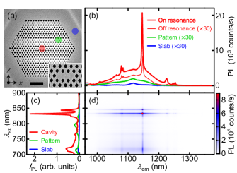
Our devices are L-type cavities in hexagonal lattice photonic crystal slabs made from silicon-on-insulator wafers Iwamoto et al. (2007); Watahiki et al. (2012). Electron beam lithography followed by a dry etching process defines the air holes in the 200-nm-thick top Si layer. We have designed the air hole radius to be where is the lattice constant. Linear defects are introduced to form L cavities, where denotes the number of missing holes. Subsequent selective wet etching removes the 1000-nm-thick buried oxide layer, thereby forming a free-standing photonic crystal membrane. Scanning electron micrographs of a typical device are shown in Fig. 1(a).
The cavities are characterized with a laser-scanning confocal microscope Moritsubo et al. (2010); Watahiki et al. (2012). A wavelength-tunable continuous-wave Ti:sapphire laser allows for PL excitation (PLE) spectroscopy, and PL images are acquired by scanning the laser beam with a fast steering mirror. An objective lens with a numerical aperture (NA) of 0.8 focuses the excitation laser beam on the sample to a spot size of 1 m, and the same lens collects the PL from silicon. Linear polarization of the excitation laser can be rotated using a half-wave plate placed just before the objective lens. A single-grating spectrometer disperses PL onto a liquid-nitrogen-cooled InGaAs photodiode array for detection. All measurements are done in air at room temperature.
Typical PL spectra are shown in Fig. 1(b) for excitation with its electric field polarized along the -axis and an incident power mW. The thin red line is the spectrum taken with the laser spot on the cavity at an excitation wavelength nm, clearly showing a cavity mode at an emission wavelength nm with a quality factor , which is assigned to the 5th mode of the L3 defect Fujita et al. (2008). Interestingly, when is tuned to 832 nm, we observe 50-fold increase in the PL intensity throughout the spectrum (thick red line).
In order to study this effect in detail, PLE spectroscopy is performed [Figs. 1(c) and 1(d)]. We see a clear “cross” pattern in the PLE map taken at the cavity [Fig. 1(d)], where the vertical line corresponds to the cavity mode in resonance with emission, while the horizontal line represents a resonance in the excitation wavelength. At the intersection, we have a double resonance, where both excitation and emission are resonant. In Fig. 1(b), the double resonance condition is met at the strongest peak in the thick red curve, and we find that the detected PL peak intensity is enhanced by a factor of 2400 compared to an unetched part of the Si slab (blue curve) at the same wavelength.
We characterize the excitation resonance using PLE spectra obtained by plotting the integrated PL intensity as a function of [Fig. 1(c), red curve]. The spectral integration has been performed over a 40-nm window centered at nm to eliminate the effects of the cavity modes. There are several sharp peaks on top of a broad spectral feature, and the strongest excitation resonance at nm has .
Such high- resonances cannot be attributed to cavity modes that are confined by the photonic band gap, as the high-energy band edge is located at around 1100 nm for this lattice constant Fujita et al. (2008). At shorter wavelengths, guided modes exist which allow photons to freely propagate in the plane of the photonic crystal slab. These guided modes can couple to free-space modes if they exist above the light line Ochiai and Sakoda (2001) and can enhance light emission over a large area because they are delocalized Fujita et al. (2008); Noda (2010).
We evaluate the effects of the guided modes by performing measurements within the photonic crystal pattern but away from the cavity. The green curve in Fig. 1(b) shows a PL spectrum with some enhancement compared to the emission from the unetched slab area, although the enhancement is significantly smaller than that observed at the cavity. A PLE spectrum on the pattern [Fig. 1(c), green curve] shows a broad spectral feature which is expected for guided modes because they have angle-dependent frequency Ochiai and Sakoda (2001) and excitation with a high NA lens would couple to a wide range of frequencies. We note that the high- resonances are absent in this spectrum, suggesting that they are only observed near the defect.
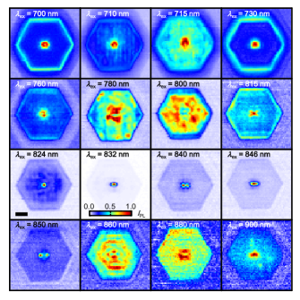
The spatial extent of the high- excitation resonances are investigated by performing imaging measurements. In Fig. 2, we present PL images taken at 16 different excitation wavelengths. As the emission spectral integration window has been chosen not to include the cavity modes, these images mostly reflect the excitation efficiency profiles. The images change drastically for the different wavelengths, and an image taken at nm shows that the PL enhancement occurs throughout the photonic crystal pattern, consistent with the delocalized nature of the guided modes. In comparison, it is clear that the high- excitation resonances at nm and 846 nm are highly localized at the defect. Similar localized resonances can be seen at other wavelengths as well, although the PL enhancements are smaller.
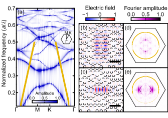
In order to identify the physical origin of the high- excitation resonances, three-dimensional finite-difference time-domain (FDTD) calculations are performed. Figure 3(a) shows the photonic band diagram for transverse-electric modes in a defect-free hexagonal-lattice photonic crystal slab. The band gap is formed at normalized frequencies to 0.33, where is the free-space wavelength. The strongest excitation resonance at nm observed in the experiments corresponds to a normalized frequency of 0.445, far above the band gap. Looking at the band diagram near this frequency, several modes exist above the light line around the point. Calculations have shown that these modes can be weakly bound to a defect to form a localized state with a reasonably high Lin and Vučković (2010).
Using FDTD simulations, we have searched for such localized states bound to an L3 defect. Indeed, several modes have been identified, and Fig. 3(b) shows field distribution for an -polarized resonance with a mode volume and . The mode profile shows that the field is localized at the defect, consistent with the results of imaging measurements. In addition, the mode has a normalized frequency which is in the vicinity of the strongest resonance observed in the experiments. Although precise mode assignment is difficult at these frequencies because of dispersion and absorption effects, the characteristics of the excitation resonances can be explained by the simulated mode. With a reasonable agreement between calculations and experiments, we attribute the high- excitation resonances to localized guided modes (LGMs). We have also performed calculations for -polarization [Fig. 3(c)], and have found LGMs at similar frequencies.
The spatial Fourier transform of the mode profile gives additional insight to the origin of the LGMs. As shown in Fig. 3(d), the -polarized mode has most of its amplitude within the light line, which implies good coupling to free-space modes. It can also be seen that there are two points with intense amplitudes above and below the zone center. Such a reciprocal space distribution suggests a simple interpretation that this LGM consists of linear combinations of unbound guided-modes. It is reasonable that reciprocal space amplitude shows high intensities at points along the -axis, because these guided-modes are -polarized. As expected from this picture, the spatial Fourier transform of the -polarized mode [Fig. 3(e)] shows strong amplitudes for wave vectors along the -axis.
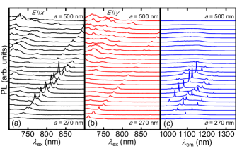
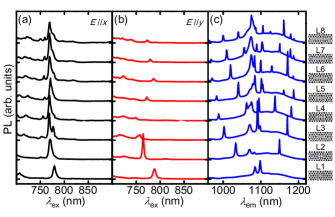
Now we consider how the LGMs can be controlled. We expect the resonances to shift linearly with the lattice constant, as they should depend on the photonic band structure. In Fig. 4(a), we present -dependence of PLE spectra from L3 defects taken with -polarized excitation. Indeed, the LGMs can be tuned over more than 100 nm by changing the lattice constant. In addition to the two prominent resonances observed for the device with nm, we observe a few other series of weaker resonances. For larger lattice constants, we observe an emergence of a broader spectral structure at shorter wavelengths, likely composed of many peaks. This is reasonable as the band structure becomes more complicated for higher normalized frequencies Fujita et al. (2008).
We have also investigated PLE spectra under -polarized excitation [Fig. 4(b)]. Here we find excitation resonances that scale with as well, but at slightly different wavelengths compared to those observed for -polarization. For guided modes in a perfect photonic crystal, both polarizations should be degenerate at the point where coupling to free-space modes are allowed Ochiai and Sakoda (2001). As the defect reduces the symmetry of the system, such an energy splitting for different polarization is expected for the LGMs.
If tuning of a double resonance to a specific combination of two wavelengths is desired, the LGMs and cavity modes need to be controlled independently. When we change the lattice constant, however, the cavity modes also shift linearly [Fig. 4(c)]. This shows that the resonances cannot be tuned independently, and implies that the double resonance can only be moved along a line in a - plane.
In order to find a way to design doubly resonant cavities, we have investigated PLE spectra from linear defects of various lengths. Interestingly, for -polarized excitation, the LGM resonances appear at similar wavelengths despite the different cavity structures [Fig. 5(a)]. In contrast, the -polarized resonances can differ in wavelength by almost 40 nm [Fig. 5(b)]. The cavity mode spectra [Fig. 5(c)] show a complex evolution as the defect length is increased. The number of the modes increases and the resonances appear at different positions within the photonic band gap.
The lattice constant dependence and the defect length dependence of the LGMs and the cavity modes are summarized in Fig. 6. We have located the peak positions for -polarized and -polarized LGMs ( and , respectively), as well as the cavity resonance wavelength . Relatively weak intensity peaks that are hard to identify in Fig. 4 are also plotted in Figs. 6(a-c). The defect length dependence of the cavity modes are shown in Fig. 6(d), where the mode polarization have been identified by placing a linear polarizer in the collection path. Cavity size dependence of the strongest LGMs are shown in Figs. 6(e) and 6(f). It is noted that both -polarized LGMs and the cavity modes are relatively insensitive to the defect length, while the -polarized modes show large changes.
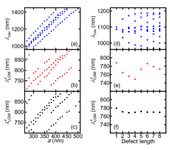
Such a different behavior depending on the polarization can be intuitively understood if we consider the LGMs as linear combinations of unbound guided modes. The -polarized modes will consist of guided modes with wave vectors along the -axis, and therefore they should be sensitive to the index of refraction profile along the -direction. Since we are comparing linear defects, the index profiles along the -axis are similar for all cavities, and it is reasonable that the LGMs appear at similar wavelengths. In comparison, for the -polarized modes, the wave vectors will be in the -direction. Changing the length of the defect directly affects the index profile that those guided waves see, and this should result in different resonant wavelengths for the -polarized modes.
The insensitivity of the -polarized LGMs to the length of the defect provides a simple procedure for tuning the double resonance to a specific combination of wavelengths. First, we can choose to tune an LGM to one wavelength, then we can look for a cavity size which has a mode at the other wavelength. Since the -polarized cavity modes are sensitive to the length of the defect, it should be possible to find a cavity mode near the desired wavelength as long as it is within the photonic band gap. Even though we are changing the defect structure in the latter step, the LGMs would have more or less the same resonance wavelength, allowing for independent tuning of the cavity modes.
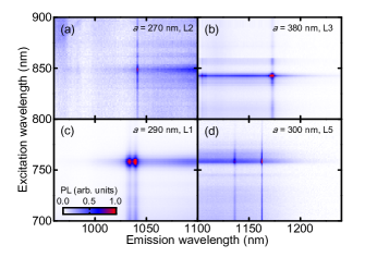
We demonstrate such flexibility in Fig. 7 by tuning the double resonance to four different combinations of excitation and emission wavelengths. First, we use the lowest normalized-frequency LGM that we have observed, which is resonant at 850 nm for nm. An L2 defect has a cavity mode at 1040 nm, producing a double resonance in the top-left corner of our PLE maps. Next, we can use an L3 cavity with nm to utilize the strong LGM at 844 nm and the 5th cavity mode at 1173 nm, obtaining a double resonance at the top-right corner. Reducing the lattice constant down to 290 nm, this LGM is now at nm, and by using an L1 cavity, the double resonance is tuned to the bottom-left corner. Finally, keeping the same LGM for excitation resonance, an L5 defect offers a cavity mode at 1162 nm, completing the last corner. The ratio of the two wavelengths for the double resonance shown in Fig. 7(d) is 1.53, comparable to those achieved in nanobeam cavities Rivoire et al. (2011a, b); Buckley et al. (2014a, b).
The flexible tuning offered by the LGM and cavity-mode double resonance should allow enhancement of emission from a wide variety of luminescent materials, such as quantum dots, molecules, fluorophores, and proteins. For emitters that show sharp resonances in absorption such as carbon nanotubes Bachilo et al. (2002), tuning the double resonance would be particularly effective. It should also be possible to enhance Raman scattering from nanoscale materials such as graphene Gan et al. (2012). Increased efficiency in wavelength conversion such as sum and difference frequency generation is expected as well, if materials with large nonlinearity are used Rivoire et al. (2011b); Buckley et al. (2014a). Although the quality factors of LGMs are smaller compared to typical cavity modes, they may be limited by the strong absorption of silicon. By using a larger electronic band gap material and an enhancement of the -factors in the L-type cavities Kuramochi et al. (2014), further increase in the efficiencies are anticipated.
In summary, we have investigated the use of LGMs for achieving doubly resonant cavities in photonic crystals, and an enhancement of silicon PL by a factor of 2400 has been demonstrated. We have characterized guided modes bound to linear defects in hexagonal lattice photonic crystal slabs using PL spectroscopy and imaging techniques, and found that LGMs have weak dependence on the defect length for one of the polarizations. Taking advantage of such a property, we have shown that the double resonance can be tuned in a flexible manner by choosing a combination of lattice constant and defect length. Our technique offers a simple method for achieving double resonance in a nanocavity, and is expected to be useful for enhancing PL and wavelength conversion at the nanoscale.
Acknowledgements.
Work supported by KAKENHI (24340066, 24654084, 26610080, 26870167), SCOPE, Canon Foundation, Asahi Glass Foundation, and KDDI Foundation, as well as the Project for Developing Innovation Systems, Nanotechnology Platform, and Photon Frontier Network Program of MEXT, Japan.References
- Joannopoulos et al. (2008) J. D. Joannopoulos, S. G. Johnson, J. N. Winn, and R. D. Meade, Photonic Crystals: Molding the Flow of Light, 2nd ed. (Princeton Univ. Press, Princeton, 2008).
- Takahashi et al. (2007) Y. Takahashi, H. Hagino, Y. Tanaka, B.-S. Song, T. Asano, and S. Noda, High- nanocavity with a 2-ns photon lifetime, Opt. Express 15, 17206 (2007).
- Sekoguchi et al. (2014) H. Sekoguchi, Y. Takahashi, T. Asano, and S. Noda, Photonic crystal nanocavity with a -factor of 9 million, Opt. Express 22, 916 (2014).
- Yoshie et al. (2001) T. Yoshie, J. Vučković, A. Scherer, H. Chen, and D. Deppe, High quality two-dimensional photonic crystal slab cavities, Appl. Phys. Lett. 79, 4289 (2001).
- Fushman et al. (2005) I. Fushman, D. Englund, and J. Vučković, Coupling of PbS quantum dots to photonic crystal cavities at room temperature, Appl. Phys. Lett. 87, 241102 (2005).
- Englund et al. (2010) D. Englund, B. Shields, K. Rivoire, F. Hatami, J. Vučković, H. Park, and M. D. Lukin, Deterministic coupling of a single nitrogen vacancy center to a photonic crystal cavity, Nano Lett. 10, 3922 (2010).
- Watahiki et al. (2012) R. Watahiki, T. Shimada, P. Zhao, S. Chiashi, S. Iwamoto, Y. Arakawa, S. Maruyama, and Y. K. Kato, Enhancement of carbon nanotube photoluminescence by photonic crystal nanocavities, Appl. Phys. Lett. 101, 141124 (2012).
- Noda et al. (2007) S. Noda, M. Fujita, and T. Asano, Spontaneous-emission control by photonic crystals and nanocavities, Nature Photon. 1, 449 (2007).
- Fujita et al. (2008) M. Fujita, Y. Tanaka, and S. Noda, Light emission from silicon in photonic crystal nanocavity, IEEE J. Sel. Top. Quantum Electron. 14, 1090 (2008).
- Ota et al. (2008) Y. Ota, M. Nomura, N. Kumagai, K. Watanabe, S. Ishida, S. Iwamoto, and Y. Arakawa, Enhanced photon emission and absorption of single quantum dot in resonance with two modes in photonic crystal nanocavity, Appl. Phys. Lett. 93, 183114 (2008).
- Imamura et al. (2013) S. Imamura, R. Watahiki, R. Miura, T. Shimada, and Y. K. Kato, Optical control of individual carbon nanotube light emitters by spectral double resonance in silicon microdisk resonators, Appl. Phys. Lett. 102, 161102 (2013).
- Takahashi et al. (2013) Y. Takahashi, Y. Inui, M. Chihara, T. Asano, R. Terawaki, and S. Noda, A micrometre-scale Raman silicon laser with a microwatt threshold, Nature 498, 470 (2013).
- Zhang et al. (2009) Y. Zhang, M. W. McCutcheon, I. B. Burgess, and M. Loncar, Ultra-high- TE/TM dual-polarized photonic crystal nanocavities, Opt. Lett. 34, 2694 (2009).
- McCutcheon et al. (2011) M. W. McCutcheon, P. B. Deotare, Y. Zhang, and M. Lončar, High- transverse-electric/transverse-magnetic photonic crystal nanobeam cavities, Appl. Phys. Lett. 98, 111117 (2011).
- Rivoire et al. (2011a) K. Rivoire, S. Buckley, and J. Vučković, Multiply resonant high quality photonic crystal nanocavities, Appl. Phys. Lett. 99, 013114 (2011a).
- Rivoire et al. (2011b) K. Rivoire, S. Buckley, and J. Vučković, Multiply resonant photonic crystal nanocavities for nonlinear frequency conversion, Opt. Express 19, 22198 (2011b).
- Iwamoto et al. (2007) S. Iwamoto, Y. Arakawa, and A. Gomyo, Observation of enhanced photoluminescence from silicon photonic crystal nanocavity at room temperature, Appl. Phys. Lett. 91, 211104 (2007).
- Moritsubo et al. (2010) S. Moritsubo, T. Murai, T. Shimada, Y. Murakami, S. Chiashi, S. Maruyama, and Y. K. Kato, Exciton diffusion in air-suspended single-walled carbon nanotubes, Phys. Rev. Lett. 104, 247402 (2010).
- Ochiai and Sakoda (2001) T. Ochiai and K. Sakoda, Dispersion relation and optical transmittance of a hexagonal photonic crystal slab, Phys. Rev. B 63, 125107 (2001).
- Noda (2010) S. Noda, Photonic crystal lasers—ultimate nanolasers and broad-area coherent lasers, J. Opt. Soc. Am. B 27, B1 (2010).
- Lin and Vučković (2010) Z. Lin and J. Vučković, Enhanced two-photon processes in single quantum dots inside photonic crystal nanocavities, Phys. Rev. B 81, 035301 (2010).
- Buckley et al. (2014a) S. Buckley, M. Radulaski, J. L. Zhang, J. Petykiewicz, K. Biermann, and J. Vučković, Nonlinear frequency conversion using high-quality modes in GaAs nanobeam cavities, Opt. Lett. 39, 5673 (2014a).
- Buckley et al. (2014b) S. Buckley, M. Radulaski, J. L. Zhang, J. Petykiewicz, K. Biermann, and J. Vučković, Multimode nanobeam cavities for nonlinear optics: high quality resonances separated by an octave, Opt. Express 22, 26498 (2014b).
- Bachilo et al. (2002) S. M. Bachilo, M. S. Strano, C. Kittrell, R. H. Hauge, R. E. Smalley, and R. B. Weisman, Structure-assigned optical spectra of single-walled carbon nanotubes, Science 298, 2361 (2002).
- Gan et al. (2012) X. Gan, K. F. Mak, Y. Gao, Y. You, F. Hatami, J. Hone, T. F. Heinz, and D. Englund, Strong enhancement of light-matter interaction in graphene coupled to a photonic crystal nanocavity, Nano Lett. 12, 5626 (2012).
- Kuramochi et al. (2014) E. Kuramochi, E. Grossman, K. Nozaki, K. Takeda, A. Shinya, H. Taniyama, and M. Notomi, Systematic hole-shifting of L-type nanocavity with an ultrahigh factor, Opt. Lett. 39, 5780 (2014).