Ball-grid array architecture for microfabricated ion traps
Abstract
State-of-the-art microfabricated ion traps for quantum information research are approaching nearly one hundred control electrodes. We report here on the development and testing of a new architecture for microfabricated ion traps, built around ball-grid array (BGA) connections, that is suitable for increasingly complex trap designs. In the BGA trap, through-substrate vias bring electrical signals from the back side of the trap die to the surface trap structure on the top side. Gold-ball bump bonds connect the back side of the trap die to an interposer for signal routing from the carrier. Trench capacitors fabricated into the trap die replace area-intensive surface or edge capacitors. Wirebonds in the BGA architecture are moved to the interposer. These last two features allow the trap die to be reduced to only the area required to produce trapping fields. The smaller trap dimensions allow tight focusing of an addressing laser beam for fast single-qubit rotations. Performance of the BGA trap as characterized with 40Ca+ ions is comparable to previous surface-electrode traps in terms of ion heating rate, mode frequency stability, and storage lifetime. We demonstrate two-qubit entanglement operations with 171Yb+ ions in a second BGA trap.
I Introduction
Trapped atomic ions are a leading platform in quantum information research, offering the advantages of precise optical manipulation and long qubit coherence times. The transport architecture proposed for scalable trapped-ion quantum computing Kielpinski, Monroe, and Wineland (2002) requires a complex system in which large numbers of ions are shuttled to various locations in the trap structure. Towards this goal, microfabrication techniques have enabled miniaturization of ion traps Chiaverini et al. (2005) that allow for the incorporation of arrays of microfabricated electrodes on a planar substrate (see, for example, Refs. Stick et al. (2006); Seidelin et al. (2006); Schulz et al. (2008); Allcock et al. (2010); Brady et al. (2011); Moehring et al. (2011); Wright et al. (2013)). In the typical trap, surface electrode structures are fabricated on a thin chip that sits atop a commercial ceramic pin-grid array (CPGA) carrier. To supply DC trapping potentials for each electrode, pads on the CPGA are wirebonded to pads on the trap chip. Capacitors on the surface of the chip or bonded at the perimeter of the carrier are used to filter out radio frequency (RF) pickup on the electrodes.
Existing fabrication techniques will limit scaling surface-electrode ion traps far beyond those in use today. Recent trap designs have grown to incorporate nearly 100 DC control electrodes Wright et al. (2013). For linear traps with as few as 50 electrodes Doret et al. (2012), the capacitors and bond pads can consume a majority of the overall trap chip area and perimeter, strongly constraining the layout of electrode structures and DC/RF lead traces. Wirebonds must be carefully arranged to minimize obstructions to laser access, as beams for trapping and qubit manipulation must interact with ions confined m above the chip surface. The large periphery (non-trap area) of the trap die presents geometric limitations to focusing these lasers onto the ion while maintaining the narrow beam waists preferred for operations such as addressing individual ions in a chain or driving hyperfine Raman transitions Rohde et al. (2001); Ozeri et al. (2007); Choi et al. (2014). For example, a 729 nm beam for single qubit addressing, focused to a waist of 3.4 m as in Ref. Rohde et al. (2001), has a Rayleigh range of 0.05 mm and would diverge to a beam radius of 100 m within 1.5 mm, incompatible with existing traditional surface trap dimensions. Novel trap architectures remove portions of the trap in several dimensions but are still constrained by wirebonds along two edges Maunz et al. (2013).
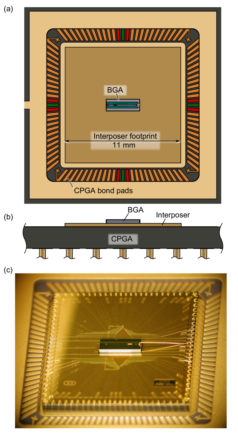
We demonstrate here a new architecture for microfabricated ion traps, built around ball-grid array (BGA) connections. Our BGA design (Fig. 1) mitigates scalability concerns related to the capacitors and wirebond connections, providing a flexible architecture for traps of increased complexity. Electrodes in the BGA trap are connected with through-substrate vias (TSVs) to pads on the back side of the trap die. Gold-ball bump bonds then connect these back-side pads to traces on an interposer. The interposer is wirebonded to a CPGA carrier for signal routing. The 100-pin Kyocera CPGA used here is compatible with our existing test setups; alternate carriers would require only a redesign of the relatively simple interposer, rather than modifications to the trap chip itself. Trench capacitors are fabricated into the trap die, similar to a proposal in Ref. Allcock et al. (2012), reducing the trap die area by a factor of thirty over traps with planar capacitors. Filter capacitors located at the edge of the CPGA would be less effective in this architecture, due to distance from the trap. With the wirebond connections relocated to the interposer, the surface of the BGA trap chip remains unobstructed for laser access. Gold is utilized for the electrode surfaces, minimizing oxide formation which is a potential source of charging and stray fields in surface electrode traps. A re-entrant metallization profile screens any trapped charge that might accrue on dielectric surfaces Harlander et al. (2010); Allcock et al. (2012). Details of the BGA trap fabrication process are provided in Section II.
We characterize the BGA trap by loading single and multiple 40Ca+ ions. Performance of the trap is comparable to previous microfabricated surface traps in terms of ion heating rate, axial mode stability, and storage lifetime for one and two trapped ions Daniilidis et al. (2011); Doret et al. (2012); Guise et al. (2014); Graham et al. (2014). We take advantage of the reduced trap die size and improved optical access to demonstrate tighter focusing of a 729 nm laser beam with resulting speedup in single-qubit rotation rates. Results from the BGA ion trap testing are presented in Section III. We present in Section IV a demonstration of two-qubit entanglement with 171Yb+ ions in a second BGA trap.
II Fabrication
II.1 Overview
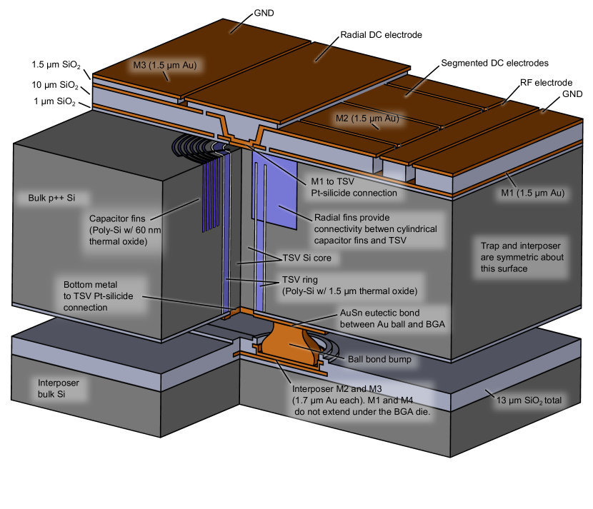
The BGA trap includes 48 trench capacitors and 48 TSVs connected to a total of 48 DC electrodes. A schematic cross section of the BGA trap is shown in Figure 2, highlighting the metal and insulator layers, trench capacitors, and TSVs. The trap die is bonded to an interposer (Sec. II.2.2), which serves to elevate the trap above the carrier for improved laser access and to route electrical connections from the package to the trap die.
II.2 Processing Details
II.2.1 Trap Die Fabrication
The process for making the trap die begins with a 500 m-thick p++ (heavily boron-doped) silicon wafer with a resistivity of cm. The key fabrication steps are described below.
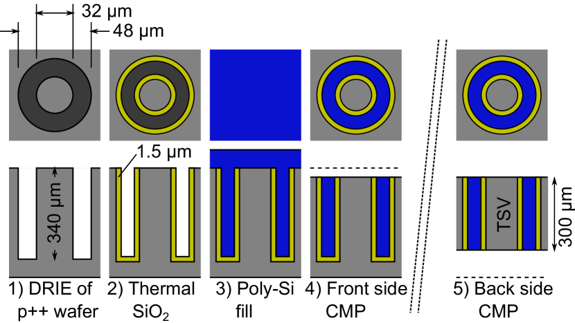
(i) Making TSVs: Figure 3 shows the complete process for forming the TSVs. Scanning electron microscope (SEM) images of the TSV features are shown in Fig. 4. The outlines for the TSVs are patterned with ring-shaped features and etched m into the wafer using a Deep Reactive Ion Etch (DRIE) tool (Fig. 3, step 1). The side and bottom walls of the TSVs are oxidized in a thermal oxidation furnace to a thickness of 1.5 m (step 2). The trenches are filled with m of highly conductive p++ polysilicon, completely sealing the tops of the holes (step 3). A Chemical Mechanical Polish (CMP) is performed from the front side to expose the original bulk silicon wafer (step 4). Much later in the fabrication process (after front-side metallization), a back-side CMP operation (step 5) reduces the wafer thickness to 300 m and exposes the TSV ring. The TSV resistances are , with breakdown voltages in excess of 380 V, above the range of the test equipment used.
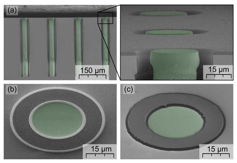
(ii) Making Trench Capacitors: Fabrication of the trench capacitors begins with DRIE of trenches arranged in concentric rings around the TSVs, 55-70 m into the silicon wafer. Thermal oxide of thickness 60 nm is grown on the sidewalls of the trenches. The trenches are then filled with p++ polysilicon. CMP is performed on the wafer surface until the bulk silicon wafer is exposed. Finally, 0.5 m of thermal SiO2 is grown to consume CMP damage. Figure 5 shows SEM images at various stages of trench capacitor fabrication. At the end of trench capacitor processing (Fig. 5d), the trench capacitors remain electrically isolated from the TSVs by a thin oxide layer.
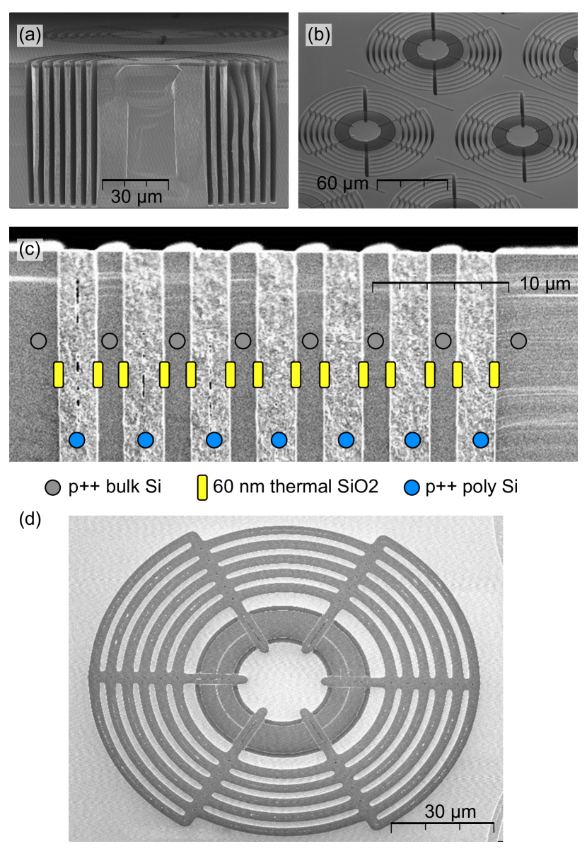
We measure capacitance values of pF for the 48 trench capacitors on a trap die. Capacitance values in the final packaged trap increase to pF, with variation dominated by differences in the lengths and widths of lead traces and electrodes. Typical breakdown voltage for a trench capacitor is V, determined by testing 100 capacitors on a test wafer.
(iii) Making Ohmic Contacts to TSVs and Trench Capacitors: Once the trench capacitors and TSVs have been formed, a 1.0 m layer of chemical vapor deposition (CVD) SiO2 is deposited on top of the wafers. A layer of photoresist is patterned connecting the TSV cores and radial arms of the trench capacitors. The wafers are then etched using a RIE (Reactive Ion Etch) process. Once the underlying silicon has been reached, we form a platinum silicide layer on the tops of the trench capacitors and TSV cores. The platinum silicide provides Ohmic contacts for electrical connections between the doped silicon structures (TSVs and associated trench capacitors) and the front-side metallization layers described below.
(iv) Patterning Metal Layers: The three front-side metallization and dielectric layers are shown schematically in Fig. 2. The bottom most metal layer (M1) is essentially a large ground plane, interrupted only where there are TSVs. The second metal layer (M2) forms the trap DC and RF electrodes. A 10 m oxide layer between M1 and M2 limits the capacitance of the RF electrodes. We utilize a third metal layer (M3) so that the M1 to TSV connection can be planarized with oxide, which prevents topography caused by that connection from affecting the ion trapping potentials. M3 contains the radial DC electrodes and a ground plane. Appendix A.1 provides additional fabrication details of the front-side metallization.
After M3 is patterned, a hour RIE step anisotropically removes exposed SiO2 by etching in the vertical direction. A 3 m BOE (Buffered Oxide Etch) process then etches the SiO2 laterally, leaving overhanging metal features which aid in screening dielectric from laser light during trap operation and which shield the ion to some extent from stray fields caused by trapped charge on the dielectrics.
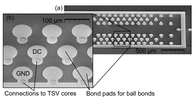
On the back side of the trap die (Fig. 6), 48 silicided contacts make electrical connections to the cores of the TSVs and to bond pads; 28 contacts make ground connections to the bulk silicon part of the die. Gold and tin are deposited on the bond pads for gold/tin eutectic solder-bonding to the interposer (Sec. II.3).
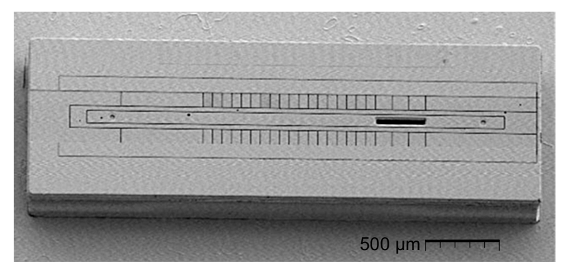
(v) Making Loading Slots: Slots in the trap die allow passage of a thermal flux of neutral atoms for ion loading (Sec. III.1). The loading slot is coated with gold to minimize the potential for charge build-up. The etch that defines the loading slots also opens up the perimeters of each die so that the die are singulated (separated from one another and from the bulk wafer). Figure 7 shows a completed trap die after it has been removed from its carrier wafer.
II.2.2 Interposer Processing
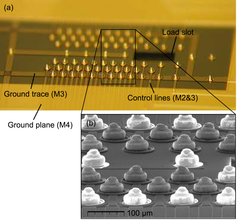
The interposer is a separate die (1 cm 1 cm by 1.3 mm-thick) whose purpose is to elevate the trap die above the rim of the package and to carry electrical signals from the package to the trap die. Signals are routed on two metal layers (Interposer M3 and M2 in Fig. 2), each 1.7 m Au with Ti and Pt adhesion/barrier layers above and below. Top and bottom ground layers (Interposer M4 and M1), each 1.7 m Au, provide electrical shielding. Slots for ion loading are DRIE-etched 300-350 m into the front side of the interposer wafer and 1000 m in from the back side, meeting to create a continuous opening that aligns with the loading slot in the trap die. Appendix A.2 provides details of the interposer fabrication process.
II.3 Assembly
For final assembly of the ion trap, we bond together the separately fabricated trap die and interposer, then package the combined unit into a CPGA carrier. A conventional gold ball bonder, programmed to leave short bond wires ( m from base to tip), attaches gold studs to the bond pads on top of the interposer (Fig. 8). With the gold studs as interconnects, the trap die is bonded with a solder-reflow process to the interposer with previously deposited gold and tin layers acting as a gold/tin eutectic solder.
A separate layer of gold studs is placed on the base of the CPGA package, and the interposer (plus trap) is ultrasonically bonded to the CPGA. Wirebonds are then attached from the CPGA to the interposer. One wire bond goes directly from the interposer to the trap die, providing a low-resistance routing for the trap RF signal. The final packaged trap is shown in Figure 1c.
III Testing
III.1 Overview
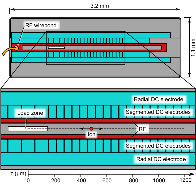
We test the BGA trap by trapping 40Ca+ ions, using techniques discussed in Refs. Doret et al. (2012); Vittorini et al. (2013). An oven located below the CPGA carrier supplies neutral Ca atoms which pass through the loading slots in the interposer and trap chip and are photoionized 60 m above the trap surface. A potential is applied to the RF electrodes (Fig. 9), where V and MHz. This creates a ponderomotive pseudopotential which confines ions radially. Ions are confined axially by applying voltages to the DC electrodes and are transported by varying these voltages to translate the axial potential minimum.
For the following measurements, the axial mode frequency (Sec. III.2) is 1.0 MHz and the radial frequencies are 4.2 MHz and 3.7 MHz. The experiments described below are performed with the ion at m (see Fig. 9).
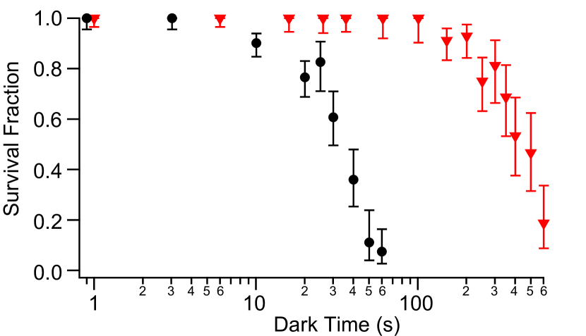
Ions are manipulated with laser light directed parallel to the trap surface. We use a 397 nm laser tuned near the transition for Doppler cooling and state detection. Fluorescence is collected onto a charge-coupled device (CCD) camera and a photomultiplier tube. An 866 nm laser repumps ions out of the metastable level. With the Doppler cooling beam on, the storage lifetime for a Ca+ ion is several hours. With the Doppler cooling beam mechanically shuttered, the ion dark lifetime (50% average survival fraction) is 450 s for a single trapped ion (Fig. 10).
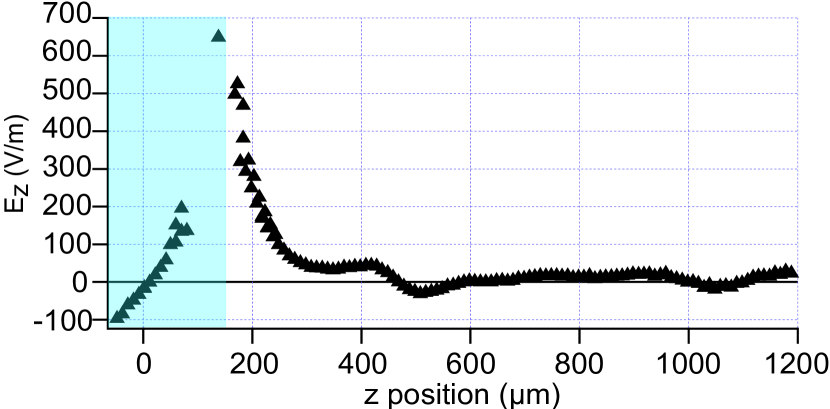
By measuring shifts in the ion equilibrium position as the harmonic trapping potential is varied, we map out stray axial electric field strength over the length of the trap (Fig. 11). We are able to trap and transport the ion within a 1.2 mm region. Stray fields near the load zone edge reach several hundred V/m but drop well below 100 V/m at a distance of 100 m from the load slot. These axial stray fields are comparable to those measured in earlier surface-electrode traps Doret et al. (2012); Guise et al. (2014); Narayanan et al. (2011).
III.2 Motional Modes
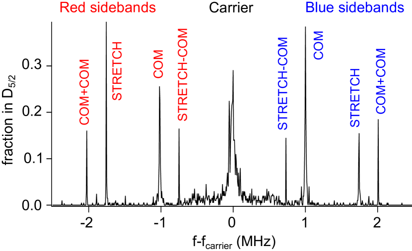
To characterize the ion’s secular frequencies, we investigate motional sidebands of the trapped ion around a motion-independent carrier frequency. The chosen carrier is an electric quadrupole transition, , with wavelength 729 nm. We apply a weak magnetic field of gauss to split the Zeeman sublevels. The carrier frequency shifts in direct proportion to magnetic field strength; we use an active compensation coil, driven by feedback from a field probe near the trap, to null out slow B field drift including 60 Hz line noise. Fig. 12 shows the spectrum around our carrier transition. Various sidebands appear due to trapped ion motion relative to the driving laser field. Axial sidebands of 1st order ( MHz) and 2nd order () are clearly resolved along with sidebands at the radial secular frequencies 4.2 MHz and 3.7 MHz.
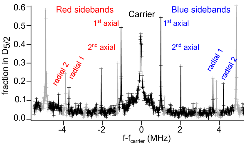
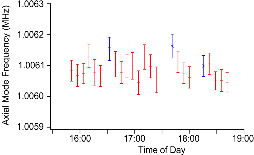
Axial mode stability is measured by repeatedly scanning over the axial red and blue sideband transitions (labeled “1st axial” in Fig. 12). The axial mode frequency remains within a range of 200 Hz (0.02%) over three hours (Fig. 13). Small shifts of Hz (0.01%) are observed due to ion reload events, which may result from charging of the trap surface by the loading beams. These reload shifts typically decay on a timescale of 5-10 minutes.
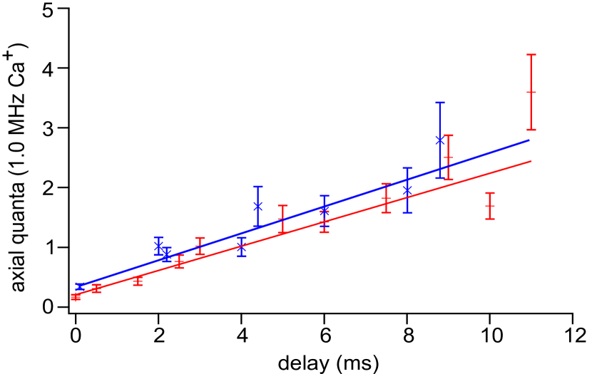
We use the average phonon occupation number in the axial mode to determine ion heating rates. For low temperatures, may be measured by comparing strengths of the 1st axial red and blue sidebands; i.e. where is the ratio of sideband strengths Turchette et al. (2000). The ion is sideband cooled to , then allowed to sit without any cooling for a controlled duration. Following the delay, is remeasured to determine the heating. Results of this measurement are shown in Fig. 14. A weighted linear fit to the data gives a heating rate of 0.21(1) quanta/ms. To check for additional heating due to ion transport, we repeat the experiment with continuous transport of the ion during the delay time. The transport rate is 0.3 m/s over a 300 m region of the trap (round trips between m and m). Transport of the ion in this manner does not affect the measured heating rate within our measurement uncertainty (blue points and fit in Fig. 14). The corresponding frequency-scaled electric field noise density, Vm2, is comparable to previous traps with similar ion-electrode separation Daniilidis et al. (2011).
III.3 Multiple Ions
We load multiple-ion chains in a single potential well (Fig. 15). After calibrating transport waveforms to correct for stray electric fields in the direction (Fig. 11), we reliably co-transport multiple ions out of the load slot to our experiment zone at m. Transport success rates are near 100% for co-transport of two or three ions at speeds of 0.33 m/s or slower.

In the experiment zone, the two-ion storage lifetime is typically 1-2 hours with Doppler cooling and 35 seconds without (Fig. 10). Note that for a two-ion chain we define lifetime by the loss of either ion. The two-ion center-of-mass (COM, MHz) and stretch ( MHz) axial sidebands are identified in Fig. 16. In preparation for two-qubit operations, we sideband cool both axial modes to near the motional ground state, quanta in each mode.
III.4 Beam Focusing
A key advantage of the BGA architecture is the possibility to focus laser beams more tightly on the ion. Tighter focus of a gate beam can speed up qubit rotation times by increasing intensity at the ion while also reducing crosstalk to neighboring ions. A focused Gaussian beam will diverge in inverse proportion to the ultimate beam waist; that is, a beam tightly focused above the trap surface will exhibit large angular spread as it enters and exits the trapping region. The dimensions of the trap chip and carrier thus impose a limit on how tightly we may focus the beam before scattering off some surface enroute.
We use various lens combinations to focus our 729 nm gate beam onto the trapped ion. The carrier Rabi rate for single qubit rotations is proportional to the amplitude of the driving electric field (square root of laser intensity) at the ion. The laser beam profile is measured by translating the ion while holding the 729 nm laser fixed and measuring the associated Rabi frequency; beam waist radius is defined as the half-width of intensity profile. Results for four different beam waists are shown in Fig. 17. The 729 nm beam is incident at 45∘ to the trap axis, giving rise to a factor of between the physical beam waists and the effective beam waists as measured by this technique.
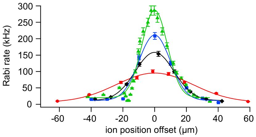
We model these results by measuring the collimated input beam with a beam profiler, then treating the focusing lenses as ideal optical elements to calculate effective beam waists at the ion. The tightest waist shown in Fig. 17 represents the approximate limit of beam focusing over the BGA trap; at 8 m waist our model indicates the beam will begin to clip on the CPGA carrier edge, resulting in a loss of a few percent of the beam power (Table 1). Deviations from the Gaussian fit are evident in the wings of the 8 m beam (green) in Fig. 17, indicating beam distortion. Beam waists of 10 m or larger, meanwhile, are predicted to experience less than 1% power loss due to clipping. For comparison, the ion separation distance for two co-trapped ions is roughly 6 m. As shown in Table 1, such tight beam focusing far exceeds what could be achieved with the same optics in a previous GTRI trap design with larger trap chip area.
| Power loss due to beam clipping | ||
| nm beam waist | ||
| (m) | in BGA trap | in Gen-V trap |
| 24.1 | % | 6.4% |
| 12.2 | 0.05% | 21.0% |
| 9.3 | 0.6% | 26.9% |
| 7.4 | 3.1% | 32.4% |
IV Entangling gates
Two qubit entangling gates in Ca+ are highly sensitive to magnetic field noise in the laboratory. Subsequent to the Ca+ testing (Sec. III), we trapped 171Yb+ in a second BGA trap (see Refs. Balzer et al. (2006); Olmschenk et al. (2007) and references therein for details on 171Yb+). The to clock transition of 171Yb+ is magnetic field insensitive at zero field and these states serve as our and qubit states, respectively. We trap pairs of qubits at z = 548 m with axial frequency 0.6 MHz and radial frequencies 1.7 MHz and 2.1 MHz. Following the work in Refs. Hayes et al. (2010); Campbell et al. (2010); Islam et al. (2014), we span the hyperfine qubit with a pulsed 355 nm Raman laser. The Raman lasers are counter propagating along the surface of the trap with approximately 10 mW in the first beam at a waist of 15 m and 30 mW in the second beam at a waist of 7 m.
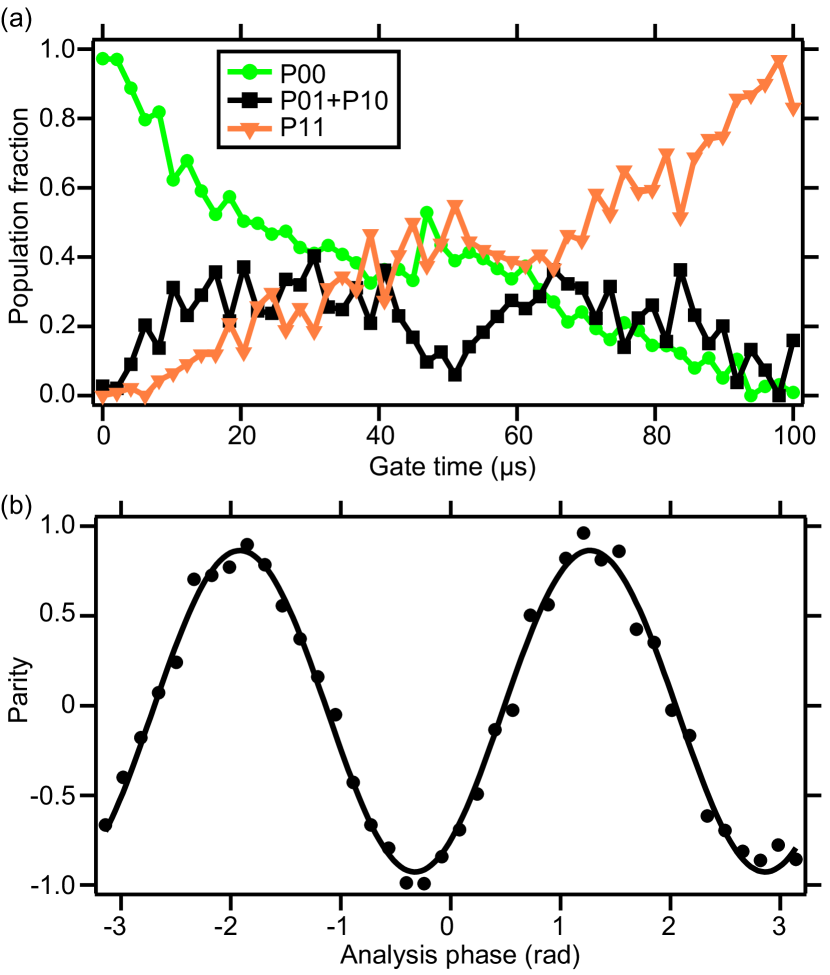
Starting in the state, we implement a Mølmer-Sørensen gate Sørensen and Mølmer (2000) on the 1.7 MHz radial mode to entangle the two ions into the state . Figure 18 shows the population evolution during the entangling gate. It also shows the parity signal at a gate time of 50 s as a function of the phase of a subsequent pulse on the carrier transition. Following Ref. Sackett et al. (2000), the resulting two qubit entanglement fidelity is 93(2)%.
V Summary and Conclusions
A ball-grid array architecture offers significant improvements in size and scalability for microfabricated ion traps. Trench capacitors fabricated into the trap die replace surface filter capacitors, providing a reduction in trap die area over traps with planar capacitors. Through-substrate vias connect the electrodes to pads on the back side of the trap die, eliminating wirebonds from the trap surface. The trap die is bump-bonded to a separate interposer chip for signal routing to a CPGA carrier. Optical access to a trapped ion is improved by the reduced BGA trap chip area and the absence of wirebond obstructions, allowing tighter focusing of laser beams for qubit operations and addressing.
BGA ion trap performance is characterized with 40Ca+ ions. We measure stray axial electric fields, motional mode stability, heating rate with and without ion transport, and dark lifetimes for one and two ions. By all measures, the BGA trap equals or exceeds results from earlier GTRI surface-electrode traps fabricated with aluminum electrodes and standard wirebonding Doret et al. (2012); Guise et al. (2014) and the heating rate is competitive with most microfabricated traps from other groups Brownnutt et al. (2014). We demonstrate focusing of an addressing 729 nm laser beam to a waist of m, approaching the separation distance for two co-trapped ions, with minimal power loss due to scattering off trap surfaces. Further improvements in ion addressing could be obtained with cylindrical optics to tighten focus along the trap axis while maintaining beam divergence in the vertical direction relevant to scattering loss. In a second BGA trap, we demonstrate a Mølmer-Sørensen gate with 93% entanglement fidelity, enabled by tight focusing of 355 nm Raman beams onto a pair of 171Yb+ ions.
Primary challenges in fabricating the BGA trap involve the trap-to-interposer ball bonding and the TSVs. An ultrasonic process proved unreliable for bonding the trap to the interposer without damaging the die; the solder reflow process described in Sec. II.3 was developed as a robust alternative. The doped silicon TSV process (Sec. II.2.1i) was developed to mitigate risks encountered in fabricating lower-resistance metal vias. In particular, filling the narrow via holes with plated metal can create voids that trap small amounts of air and degrade the ultra-high vacuum trap environment.
The BGA architecture extends readily to traps of increasing complexity. BGA techniques could simplify fabrication of intricate junction traps, such as the NIST Racetrack Amini et al. (2010) and Sandia MUSIQC Circulator Monroe and Kim (2013), which feature rings of RF rails encircling isolated islands of control electrodes; in such designs it becomes impossible to route leads to all electrodes on a single metal layer. BGA interposer design is flexible and easily modified for signal routing from carriers other than the standard CPGA presented here. The BGA architecture could be integrated with recently demonstrated in-vacuum electronics Guise et al. (2014) to produce ion traps with significantly larger numbers of electrodes at manageable physical size.
VI ACKNOWLEDGMENTS
This material is based upon work supported by the Office of the Director of National Intelligence (ODNI), Intelligence Advanced Research Projects Activity (IARPA) under U.S. Army Research Office (ARO) contracts W911NF1210605 and W911NF1010231. All statements of fact, opinion, or conclusions contained herein are those of the authors and should not be construed as representing the official views or policies of IARPA, the ODNI, or the U.S. Government.
Appendix A Fabrication Details
A.1 Trap Die Front-side Metallization
On the trap die, the bottom-most metal layer (M1) is a 1.5 m-thick layer of gold surrounded below by a TiW/Pt adhesion/diffusion barrier and above by a Ti adhesion layer. At the locations of TSVs, M1 is patterned into 50 m-diameter discs that are separated from the ground plane by 5 m gaps. The discs are connected to the TSVs below through Ohmic contacts and to the above metal layer (M2) by vias. The dielectric between the TSVs and M1 is 1.5 m thick; the dielectric between M1 and M2 is 10 m thick. Vias in the second dielectric are formed by thermally sloping photoresist and etching the vias in a recipe that transfers the slope into the SiO2.
M2 forms the trap DC and RF electrodes. M2 is 1.5 m of gold with 30 nm of Ti above and below to ensure good adhesion to the SiO2 dielectric. After M2 has been patterned, CVD SiO2 is deposited over the entire wafer, and a CMP operation is performed to remove most of the topography associated with M2 and the M1-to-M2 vias. After CMP an additional layer of 1.5 m of TEOS SiO2 is deposited.
The last metal layer (M3) is also 1.5 m of gold. A via is etched through the 3.5 m SiO2 prior to 3rd metal deposition. A via plug (also 3.5 m thick) is used to fill the via and thereby improve the planarity of the 3rd metal surface. There is minimal print-through into M3 of features other than the via plugs. A temporary layer of Ti and Pt protects M3 during the subsequent oxide etch.
A.2 Interposer Fabrication
The process for making the interposer is summarized below, with some detail shown in Figures 2 and 8.
-
1.
Interposer M1 (first metallization layer): M1 forms a uniform ground plane beneath the signal carrying lines excluding the region under the BGA, which is left as bare silicon. M1 is 1.7 m of Au, with Ti and Pt adhesion/barrier layers above and below. A blanket layer of 4 m of SiO2 is deposited above.
-
2.
Interposer M2 (second metallization layer): M2, also 1.7 m of Au surrounded by Ti and Pt, carries signals from M3 (see below) to the ball bonds under the BGA. This allows the control signals to pass under ground connections made on M3. A blanket layer of 6 m of SiO2 is deposited above.
-
3.
First via: The first via process etches holes through the SiO2 dielectric down to the metal layer beneath. In cases where there is a feature on M2 under the via, the etch stops on M2. Otherwise the etch continues down to M1 (ground).
-
4.
Interposer M3 (third metallization layer): M3 (1.7 m Au) carries signals to M2 from the edges of the interposer and grounds a series of ball bonds on the perimeter of the BGA. The grounded ball bonds provide a low impedance ground path between the BGA and the interposer. A blanket layer of 3 m of SiO2 is deposited above.
-
5.
Second via: The second via process opens up holes though the 3 m of SiO2 down to M3. Holes near the perimeter of the interposer expose pads on M3 for wire-bonding to the package. Holes near the center of the interposer expose pads on M3 for solder-bonding to the trap die.
-
6.
Interposer M4 (fourth metallization layer): M4 (1.7 m Au) is a ground plane covering the bulk of the die except for the region under the BGA.
-
7.
Bond pads: An additional layer of metal is deposited, with thickness and properties optimized for bonding.
-
8.
Front-side loading slots: Holes for the ion loading slots are DRIE-etched 300-350 m into the front side of the wafer.
-
9.
Back-side loading slots: Holes for the ion loading slots are DRIE-etched 1000 m in from the back side of the wafer, meeting the front-side loading slot holes 300 m from the front surface of the interposer to create a continuous opening.
References
- Kielpinski, Monroe, and Wineland (2002) D. Kielpinski, C. Monroe, and D. J. Wineland, “Architecture for a large-scale ion-trap quantum computer,” Nature 417, 709–711 (2002).
- Chiaverini et al. (2005) J. Chiaverini, R. B. Blakestad, J. Britton, J. D. Jost, C. Langer, D. Leibfried, R. Ozeri, and D. J. Wineland, “Surface-electrode architecture for ion-trap quantum information processing,” Quantum Inf. Comput. 5, 419 (2005).
- Stick et al. (2006) D. Stick, W. K. Hensinger, S. Olmschenk, M. J. Madsen, K. Schwab, and C. Monroe, “Ion trap in a semiconductor chip,” Nature Physics 2, 36 (2006).
- Seidelin et al. (2006) S. Seidelin, J. Chiaverini, R. Reichle, J. J. Bollinger, D. Leibfried, J. Britton, J. H. Wesenberg, R. B. Blakestad, R. J. Epstein, D. B. Hume, W. M. Itano, J. D. Jost, C. Langer, R. Ozeri, N. Shiga, and D. J. Wineland, “Microfabricated surface-electrode ion trap for scalable quantum information processing,” Phys. Rev. Lett. 96, 253003 (2006).
- Schulz et al. (2008) S. A. Schulz, U. Poschinger, F. Ziesel, and F. Schmidt-Kaler, “Sideband cooling and coherent dynamics in a microchip multi-segmented ion trap,” New Journal of Physics 10, 045007 (2008).
- Allcock et al. (2010) D. T. C. Allcock, J. A. Sherman, D. N. Stacey, A. H. Burrell, M. J. Curtis, G. Imreh, N. M. Linke, D. J. Szwer, S. C. Webster, A. M. Steane, and D. M. Lucas, “Implementation of a symmetric surface-electrode ion trap with field compensation using a modulated Raman effect,” New Journal of Physics 12, 053026 (2010).
- Brady et al. (2011) G. Brady, A. Ellis, D. Moehring, D. Stick, C. Highstrete, K. Fortier, M. Blain, R. Haltli, A. Cruz-Cabrera, R. Briggs, J. Wendt, T. Carter, S. Samora, and S. Kemme, “Integration of fluorescence collection optics with a microfabricated surface electrode ion trap,” Applied Physics B 103, 801–808 (2011).
- Moehring et al. (2011) D. L. Moehring, C. Highstrete, D. Stick, K. M. Fortier, R. Haltli, C. Tigges, and M. G. Blain, “Design, fabrication and experimental demonstration of junction surface ion traps,” New Journal of Physics 13, 075018 (2011).
- Wright et al. (2013) K. Wright, J. M. Amini, D. L. Faircloth, C. Volin, S. C. Doret, H. Hayden, C.-S. Pai, D. W. Landgren, D. Denison, T. Killian, R. E. Slusher, and A. W. Harter, “Reliable transport through a microfabricated x -junction surface-electrode ion trap,” New J. Phys. 15, 033004 (2013).
- Doret et al. (2012) S. C. Doret, J. M. Amini, K. Wright, C. Volin, T. Killian, A. Ozakin, D. Denison, H. Hayden, C. Pai, R. E. Slusher, and A. W. Harter, “Controlling trapping potentials and stray electric fields in a microfabricated ion trap through design and compensation,” New J. Phys. 14, 073012 (2012).
- Rohde et al. (2001) H. Rohde, S. T. Gulde, C. F. Roos, P. A. Barton, D. Leibfried, J. Eschner, F. Schmidt-Kaler, and R. Blatt, “Sympathetic ground-state cooling and coherent manipulation with two-ion crystals,” Journal of Optics B: Quantum and Semiclassical Optics 3, S34 (2001).
- Ozeri et al. (2007) R. Ozeri, W. M. Itano, R. B. Blakestad, J. Britton, J. Chiaverini, J. D. Jost, C. Langer, D. Leibfried, R. Reichle, S. Seidelin, J. H. Wesenberg, and D. J. Wineland, “Errors in trapped-ion quantum gates due to spontaneous photon scattering,” Phys. Rev. A 75, 042329 (2007).
- Choi et al. (2014) T. Choi, S. Debnath, T. A. Manning, C. Figgatt, Z.-X. Gong, L.-M. Duan, and C. Monroe, “Optimal quantum control of multimode couplings between trapped ion qubits for scalable entanglement,” Phys. Rev. Lett. 112, 190502 (2014).
- Maunz et al. (2013) P. Maunz, M. Blain, F. Benito, C. Chou, C. Clark, M. Descour, R. Ellis, R. Haltli, E. Heller, S. Kemme, J. Sterk, B. Tabakov, C. Tigges, and D. Stick, “Surface ion trap structures with excellent optical access for quantum information processing,” Bulletin of the American Physical Society 58 (2013).
- Allcock et al. (2012) D. Allcock, T. Harty, H. Janacek, N. Linke, C. Ballance, A. Steane, D. Lucas, J. Jarecki, R.L., S. Habermehl, M. Blain, D. Stick, and D. Moehring, “Heating rate and electrode charging measurements in a scalable, microfabricated, surface-electrode ion trap,” Applied Physics B 107, 913–919 (2012).
- Harlander et al. (2010) M. Harlander, M. Brownnutt, W. Hänsel, and R. Blatt, “Trapped-ion probing of light-induced charging effects on dielectrics,” New Journal of Physics 12, 093035 (2010).
- Daniilidis et al. (2011) N. Daniilidis, S. Narayanan, S. A. Möller, R. Clark, T. E. Lee, P. J. Leek, A. Wallraff, S. Schulz, F. Schmidt-Kaler, and H. Häffner, “Fabrication and heating rate study of microscopic surface electrode ion traps,” New Journal of Physics 13, 013032 (2011).
- Guise et al. (2014) N. D. Guise, S. D. Fallek, H. Hayden, C.-S. Pai, C. Volin, K. R. Brown, J. T. Merrill, A. W. Harter, J. M. Amini, L. M. Lust, K. Muldoon, D. Carlson, and J. Budach, “In-vacuum active electronics for microfabricated ion traps,” Review of Scientific Instruments 85, 063101 (2014).
- Graham et al. (2014) R. D. Graham, S.-P. Chen, T. Sakrejda, J. Wright, Z. Zhou, and B. B. Blinov, “A system for trapping barium ions in a microfabricated surface trap,” AIP Advances 4, 057124 (2014).
- Vittorini et al. (2013) G. Vittorini, K. Wright, K. R. Brown, A. W. Harter, and S. C. Doret, “Modular cryostat for ion trapping with surface-electrode ion traps,” Review of Scientific Instruments 84, 043112 (2013).
- Narayanan et al. (2011) S. Narayanan, N. Daniilidis, S. A. Möller, R. Clark, F. Ziesel, K. Singer, F. Schmidt-Kaler, and H. Häffner, “Electric field compensation and sensing with a single ion in a planar trap,” Journal of Applied Physics 110, 114909 (2011).
- Turchette et al. (2000) Q. A. Turchette, D. Kielpinski, B. E. King, D. Leibfried, D. M. Meekhof, C. J. Myatt, M. A. Rowe, C. A. Sackett, C. S. Wood, W. M. Itano, C. Monroe, and D. J. Wineland, “Heating of trapped ions from the quantum ground state,” Phys. Rev. A 61, 063418 (2000).
- Balzer et al. (2006) C. Balzer, A. Braun, T. Hannemann, C. Paape, M. Ettler, W. Neuhauser, and C. Wunderlich, “Electrodynamically trapped Yb+ ions for quantum information processing,” Phys. Rev. A 73, 041407 (2006).
- Olmschenk et al. (2007) S. Olmschenk, K. C. Younge, D. L. Moehring, D. N. Matsukevich, P. Maunz, and C. Monroe, “Manipulation and detection of a trapped Yb+ hyperfine qubit,” Phys. Rev. A 76, 052314 (2007).
- Hayes et al. (2010) D. Hayes, D. N. Matsukevich, P. Maunz, D. Hucul, Q. Quraishi, S. Olmschenk, W. Campbell, J. Mizrahi, C. Senko, and C. Monroe, “Entanglement of atomic qubits using an optical frequency comb,” Phys. Rev. Lett. 104, 140501 (2010).
- Campbell et al. (2010) W. C. Campbell, J. Mizrahi, Q. Quraishi, C. Senko, D. Hayes, D. Hucul, D. N. Matsukevich, P. Maunz, and C. Monroe, “Ultrafast gates for single atomic qubits,” Phys. Rev. Lett. 105, 090502 (2010).
- Islam et al. (2014) R. Islam, W. C. Campbell, T. Choi, S. M. Clark, C. W. S. Conover, S. Debnath, E. E. Edwards, B. Fields, D. Hayes, D. Hucul, I. V. Inlek, K. G. Johnson, S. Korenblit, A. Lee, K. W. Lee, T. A. Manning, D. N. Matsukevich, J. Mizrahi, Q. Quraishi, C. Senko, J. Smith, and C. Monroe, “Beat note stabilization of mode-locked lasers for quantum information processing,” Opt. Lett. 39, 3238–3241 (2014).
- Sørensen and Mølmer (2000) A. Sørensen and K. Mølmer, “Entanglement and quantum computation with ions in thermal motion,” Phys. Rev. A 62, 022311 (2000).
- Sackett et al. (2000) C. A. Sackett, D. Kielpinski, B. E. King, C. Langer, V. Meyer, C. J. Myatt, M. Rowe, Q. A. Turchette, W. M. Itano, D. J. Wineland, and C. Monroe, “Experimental entanglement of four particles,” Nature 404, 256–259 (2000).
- Brownnutt et al. (2014) M. Brownnutt, M. Kumph, P. Rabl, and R. Blatt, “Ion-trap measurements of electric-field noise near surfaces,” arXiv preprint arXiv:1409.6572v1 (2014).
- Amini et al. (2010) J. M. Amini, H. Uys, J. H. Wesenberg, S. Seidelin, J. Britton, J. J. Bollinger, D. Leibfried, C. Ospelkaus, A. P. VanDevender, and D. J. Wineland, “Toward scalable ion traps for quantum information processing,” New Journal of Physics 12, 033031 (2010).
- Monroe and Kim (2013) C. Monroe and J. Kim, “Scaling the ion trap quantum processor,” Science 339, 1164–1169 (2013), http://www.sciencemag.org/content/339/6124/1164.full.pdf .