Manipulating quantum channels in weak topological insulator nanoarchitectures
Abstract
In strong topological insulators protected surface states are always manifest, while in weak topological insulators (WTI) the corresponding metallic surface states are either manifest or hidden, depending on the orientation of the surface. One can design a nanostep on the surface of WTI such that a protected helical channel appears along it. In a more generic WTI nanostructure, multiple sets of such quasi-1D channels emerge and are coupled to each other. We study the response of the electronic spectrum associated with such quasi-1D surface modes against a magnetic flux piercing the system in the presence of disorder, and find a non-trivial, connected spectral flow as a clear signature indicating the immunity of the surface modes to disorder. We propose that the WTI nanoarchitecture is a promising platform for realizing topologically protected nanocircuits immune to disorder.
pacs:
71.23.-k, 71.55.Ak,I Introduction
Three-dimensional (3D) topological insulators are classified into weak and strong. Moore and Balents (2007); Fu et al. (2007); Roy (2009) The strong topological insulator (STI) exhibits a single Dirac cone in the surface Brillouin zone (BZ), which is immune to backscattering by non-magnetic impurities. Nomura et al. (2007); Bardarson et al. (2007) The immunity to backscattering also implies that an electronic state in the single Dirac cone cannot be confined in a finite area. Instead, it is extended to the entire surface of STI,Takane and Imura (2012) making all its facets metallic. On contrary, the weak topological insulator (WTI) exhibits an even number of (typically two) Dirac cones in the surface BZ, which can be confined; among surfaces of a WTI sample oriented in different directions there are also gapped surfaces. In this sense topological non-triviality is always manifest in STI, while in WTI it is either manifest or hidden. Ran et al. (2009); Imura et al. (2011a); Ringel et al. (2012); Liu et al. (2012); Imura et al. (2012); Yoshimura et al. (2013); Takane (2014); Kobayashi et al. (2014) Besides, in WTI one can actually switch it on and off. We have previously shown Yoshimura et al. (2013) that a one-dimensional (1D) helical channel emerges along a step formed on the surface of a WTI, and it can be regarded as a perfectly conducting channel (PCC) without backscattering. Using such PCCs, one can possibly construct a nano-circuit of protected 1D helical modes on the surface of WTI by simply patterning it with the use of lithography and etching. This controllability of the topological non-trivialness sometimes makes WTI more useful than STI.
An experimental realization of a WTI has been reported in a bismuth-based layered compound Bi14Rh3I9. Rasche et al. (2013) More recently, a helical 1D channel emergent on a step-like surfaces of a WTI Yoshimura et al. (2013) has been also observed experimentally.Pauly et al. (2015) Yet, in spite of the number of realizations of 3D topological insulators, Ando (2013) there have not been many proposals for realizing a WTI in stoichiometric compounds. Bahramy et al. (2012) WTI may be realized in superlattice systems. Yan et al. (2012); Fukui et al. (2013); Yang et al. (2014); Yoshimura et al. (2014) Features specific to WTI can be also seen in the so-called topological crystalline insulators (TCI). Fu (2011); Hsieh et al. (2012); Tanaka et al. (2012); Dziawa et al. (2012) Unlike the standard topological insulators protected by time-reversal symmetry, TCI is protected by crystalline symmetry.Morimoto and Furusaki (2013)
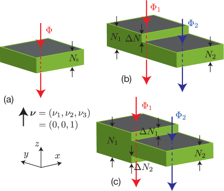
In Ref. 12, the case of a single nano-circuit emergent on a WTI surface has been analyzed in some detail. In reality, however, in the case of any realistic nano-circuit useful for application, there would be more than a single circuit, interacting with each other on the chip. Here, in this paper we highlight, in contrast to Ref. Yoshimura et al., 2013, such multi-channel cases. As a typical setup for realizing a mentioned PCC we consider patterned surfaces of a WTI film or a flake; panel (a) of Fig. 1 represents an idealized example of such nano-flake. We need a step of height corresponding to an odd number of atomic layers formed on a gapped surface [see panel (b) of Fig. 1]; a robust PCC is guaranteed to exist in this case (see Sec. II-A for a more detailed description). If the height of the step is even, the channel tends to get gapped and localized. Such an even/odd feature has been also studied in Ref. Yoshimura et al., 2013, and the arguments given there can be used to characterize a single isolated channel. However, a circuit of such a PCC is inevitably closed on a surface of WTI nanoflake reflecting its topological nature. Then, one has to consider not only the height of a step but also that of the base nano-flake. As an idealistic example we first consider the case of a single step on such a nano-flake (see Sec. IV A), before considering the more interesting case of two steps as a nontrivial example (Sec. IV B).
So far we have in mind the cases of single and double PCC nano-circuits, discussed respectively in Sec. IV A and in Sec. IV B. We analyze in these sections how they respond to disorder, localized vs. delocalized, etc. By studying response of the system against flux insertion numerically, we characterize quantum junctions at which multiple sets of quasi-1D channels meet and couple to one another under a certain “traffic rule”. Nano-circuits formed on the surface of the WTI sample are composed of different parts incident either at the step or on side surfaces of the sample. They meet typically at either end of the step region, forming a junction of quantum channels. At such junctions they are connected under the rule revealed by the above flux-insertion numerical experiment: some are strongly (smoothly) connected to form a part of PCC, others not. As a concrete example of double PCC we consider a rather specific geometry with two steps; one on the top and the other at the bottom of a nano-flake, but the obtained traffic rules could be equally applied to a more generic but topologically equivalent geometries. In a generic situation we will have multiple sets of such nano-circuits. Yet, based on the observation we establish here in the single and double PCC cases, we can naturally conjecture that characteristics of such multiple setup can be reduced to those of the single and double PCC nano-circuits. In the same sense that the single and double PCC nano-circuits are immune to backscattering by disorder, a more generic setup with multiple PCCs is also considered to be immune to disorder.
The paper is organized as follows. In Sec. II we introduce and define our model employed in the (tight-binding) numerical simulation presented in the subsequent sections. In Sec. III we discuss even/odd features in the case of a WTI nano-flake. In Sec. IV, we extend this observation to characterize different variations of the 1D helical modes emergent in WTI nano-structures, typically at a step or at steps. It is shown to be possible to realize various types of non-trivial junctions that involve 1D PCCs in WTI nano-structures. Sec. V is devoted to conclusions.
II Model
To study the robustness of 1D helical channels emergent on the surface of a WTI nano-structure, we first need to design such a nano-structure. We define our bulk effective Hamiltonian, introduce the type of random potentials distributed over the sample, and then sketch our standard recipe for performing a numerical simulation.
II.1 Bulk material: a specific type of time-reversal invariant topological insulator
Our bulk topological insulator (TI) is a standard type protected by the time reversal symmetry (TRS). It is also called a TI, since it is distinguished from the trivial band insulator by a type topological number. Kane and Mele (2005) Compared with the trivial band insulator it has an inverted band gap; this inversion is usually due to a strong spin-orbit coupling which preserves TRS. When the primary index is nonzero (i.e., ), such a TI is called a “strong” TI and exhibits a single Dirac cone on all the facets of the sample. When , we still have a possibility that the insulator is nontrivial; the secondary indices , , could be still nonzero. In the reminder of the paper we focus on cases in which our bulk material falls on the class of such a “weak” TI or WTI. The WTI exhibits generally an even number of Dirac cones on its surface, while the surface normal to the direction exhibits no gapless Dirac cone.
II.2 Model geometries
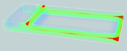
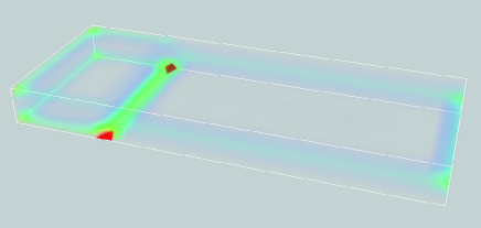
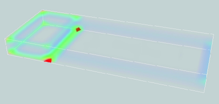
As a toy example of such a nano-architecture, we first consider the case of a WTI nano-flake, as represented in Fig. 1 (a). In the figure, the film thickness is somewhat exaggerated for clarity, and here we consider a typical and realistic situation Rasche et al. (2013) in which the top and bottom surfaces of the film are gapped. As shown in the figure, this has been encoded in the choice of weak indices: . For this case, the WTI nanofilm consists of unit atomic layers stacked in the -direction, where each layer can be regarded as a 2D quantum spin-Hall (QSH) insulator having a counter-propagating pair of 1D (gapless) helical edge channels. Let be the number of unit atomic layers. In the limit of decoupled such 2D QSH states there are pairs of 1D helical edge channels, each circulating around the corresponding 2D QSH layer. When such 2D QSH layers are coupled to form a WTI in the bulk, the corresponding 1D channels are also coupled to form surface states of the bulk WTI which appears only on side surfaces of the film. In the film geometry, here represented as a flattened rectangular prism of height , the conducting property of such WTI surface states is a drastic function of , since they are confined in a finite width of side surfaces. Takane (2004); Ringel et al. (2012); Imura et al. (2012); Kobayashi et al. (2014) If is odd, there always remain, after recombination, a single pair of helical modes that are gapless, extended and perfectly conducting: formation of the PCC in the case of odd. If is even, all the channels are gapped and tend to get localized.
Once the electronic properties of such WTI films are properly addressed, we proceed to analyzing the case of WTI terraces. In Fig. 1 (b) a simplest example of such terraces is modeled by two prisms of different heights and joined together through a side surface. A scenario similar to the nanofilm case applies to this case of single step geometry; when the height of the step is an odd-integer multiple of atomic layers, there appears a robust 1D channel along the step. Yoshimura et al. (2013) If one thinks of a more generic WTI nanostructure, multiple sets of such 1D channels are expected to appear, and couple to each other. If isolated, each set of 1D channels acts according to the even/odd rule we find in the case of the prism, while when they get together, interact, and eventually recombine, it is less trivial to tell what would happen.
In panel (c) of Fig. 1 we give an example of multiple 1D channels along steps that run in parallel; one stemming from the top, the other from the bottom surface. Let us assume that and are both odd, giving rise to 1D channels that are robust against disorder. If and are also odd, the robust 1D channels are extended to side surfaces either on the or to the side. An interesting question is how the two channels incident at the step recombine to either of the side surfaces at the junction of quantum channels formed at both ends of the step. If two channels at the step are spatially well separated () they do not interact and will act as two independent, perfectly conducting channel. In the opposite limit: , we address in this paper, two odd-number channels run in parallel close to each other. In this situation it is a priori not clear whether or not this pair of an odd-number of channels merge together to become a single set of gapped even-number channels. To probe the nature of helical modes along the step and around the side surfaces, we study response of the system to a magnetic flux. We try different ways of inserting a flux: e.g., and in Fig. 1 (c) to obtain further insight on how different 1D channels couple and recombine to each another.
II.3 Effective Hamiltonian, model parameters
To represent a bulk TI we consider the following Wilson-Dirac type effective Hamiltonian Zhang et al. (2010); Liu et al. (2010)
| (1) |
where
| (2) |
In Eqs. (1) and (2) a summation over the repeated index is not shown explicitly. Eq. (1) can be regarded as a matrix, spanned by two types of Pauli matrices and each representing physically real and orbital spins. Eq. (1) can be regarded as a lattice version of the continuum Dirac Hamiltonian
| (3) |
at the -point, where . Here, in Eqs. (1), (2) the lattice is chosen to be simple cubic for simplicity. On top of Eqs. (1), (2) we also consider on-site potential disorder of strength . On each site of the cubic lattice a random potential of magnitude is introduced, and distributed uniformly in the range of .
II.4 Numerical simulations
The tight-binding form of our model Hamiltonian (1) is also useful for implementing the real space geometries introduced in Sec. A. Indeed, Eq. (1) represents a tight-binding Hamiltonian with only onsite and nearest neighbor hopping terms defined on the cubic lattice. Then, the real space geometries as depicted in the three panels of Fig. 1 can be implemented by setting all the hopping parameters outside the designed nano-structure to be null in the real space representation of Eq. (1). In the actual implementation we can simply truncate the real space Hamiltonian into a matrix, where is the number of sites representing the nano-structure.
(a)
 (b)
(b)
(c)
 (d)
(d)
(a)
 (b)
(b)
(c)
 (d)
(d)
III WTI nanofilm: case of even vs. odd number of atomic layers
The specificity of the WTI surface states is that it has “dark” surfaces (gapped surfaces). Yoshimura et al. (2013) Below we will make the best use of this existence of the dark surfaces in the study of the robustness of edge state network against disorder. The transport character of a WTI thin film shows also a peculiar dependence (an even/odd feature) on the number of stacked atomic layers. Here, we focus on a rectangular nano-flake geometry as depicted in Fig. 1 (a), and quantify such an even/odd feature in spectrum and in the behavior of the wave function in the presence of disorder.
III.1 Response to disorder, response to the flux
A standard way to quantify the response of the system to disorder is to study the conductance in an open geometry. Kobayashi et al. (2013) But here, since our primary purpose is to examine the robustness of the edge state network against disorder, we have chosen to consider a finite, closed system with circulating quasi-1D surface states, and study their response to disorder by examining the spectral flow when an external magnetic flux is introduced piercing the system. Such an approach can be more straightforwardly adapted to the case of the edge state network. A non-trivial spectral flow is a smoking gun for the existence of a robust surface state, and is protected by the Kramers degeneracy, an immediate consequence of the time-reversal symmetry.
Note that our bulk material is in a WTI phase with specific weak indices: ; i.e., surfaces normal to the -direction (the top and bottom surfaces) are dark/gapped surfaces, so that the flux inserted (in the -direction) through such surfaces does not touch the surface states emergent on side surfaces of the system (see Fig. 1). The role of the flux is then to twist the boundary condition applied to such helical surface states circulating around the flux Ringel et al. (2012); Sbierski and Brouwer (2014) The flow of the spectrum in the presence of disorder as a function of the flux encodes information on the response of the surface states against disorder; i.e., whether the surface states are localized or extended.
In a WTI nano-flake as depicted in Fig. 1 (a) electrons in the mid-gap states are confined onto side surfaces, forming a closed 1D circuit consisting of a pair of helical modes. The electronic properties of the helical states are governed by the thickness of the flake. The even/odd feature in the clean limit is discussed in the next subsection. In the presence of disorder, such a difference in the behavior of surface 1D modes is further accentuated. When is odd, the 1D modes remain to be perfectly conducting; while, when is even, all the 1D channels tend to get localized. These two contrasting behaviors can indeed be triggered by our diagnosis focusing on the flow of the spectrum as a function of the flux inserted.
Each eigenstate on the 1D circuit is characterized by a component of momentum along the circumferential direction [see also part B, where is explicitly introduced in the formulation given there]. Naturally, is discretized, reflecting the finite circumference of the nano-flake [see Eqs. (11) and (12)] so that the energy spectrum is also discretized. The flux is here inserted through a single plaquette centered roughly at the position of the axis of the prism [see Fig. 1(a)]. An electron in the 1D surface state circulating the prism “feels” the flux inserted through the Aharonov-Bohm (AB) effect, provided, of course, that such an (extended) state is existent; in the presence of disorder this happens only in the case of odd. Introduction of the flux results in the shift of by an amount of with . As varying over one cycle of AB oscillation: , the discretized energy eigenvalues are interpolated and reconstructed; see the arguments given in the next subsection. The above arguments can be generalized, and holds also true in the presence of disorder.Buettiker et al. (1983)
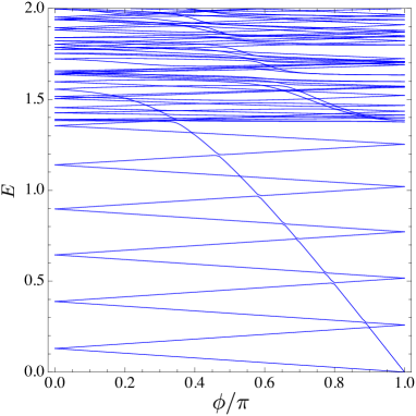
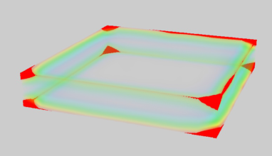
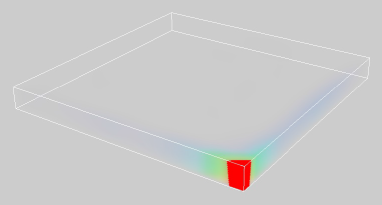
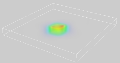
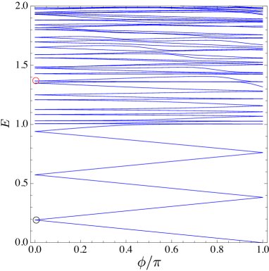
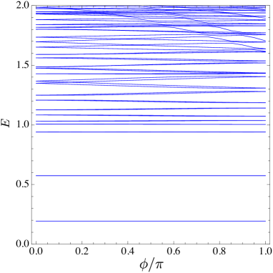
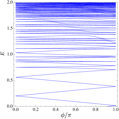
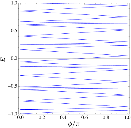
Fig. 2 (a-d) are examples of the calculated spectral flow. Panels (a), (b) deal with the clean limit, while panels (c), (d) correspond to the disordered case with (hereafter is measured in units of ). They both demonstrate the contrasting behaviors in the -dependence of the spectrum: in the cases of odd vs. even. In panels (a), (b) of Fig. 3, the contrasting behavior of typical surface wave functions are shown: when is odd [case of panel (a)], the surface wave function is extended and covers the entire side surfaces. On contrary, when is even [case of panel (b)], the surface wave function is localized in the vicinity of one corner of the prism. In the spectral shown in Fig. 2 one can also recognize a branch of spectrum due to bound states formed along the flux introduced [see also Fig. 3 (c), (d)].
III.2 Nature of the electronic states on WTI surfaces
To have further insight on the contrasting behaviors in spectral flow revealed in Fig. 2 in the cases of odd and even, we start by analyzing this issue based on the effective theory for WTI surface states. Such an effective theory has been employed in the analyses of Refs. Mong et al., 2012; Fu and Kane, 2012; Morimoto and Furusaki, 2013; Obuse et al., 2014, while more recently it has been explicitly derived from the bulk effective Hamiltonian. Arita and Takane (2014) The central ingredients of the theory are two Dirac cones that appear in the surface BZ for a side surface that is parallel to .
In the following simulations we choose the parameters as in Eq. (4) to realize a WTI with indices . We then put this system into a geometry as shown in Fig. 1 (a), i.e., a prism of height and with a constant cross sectional area of size . As a result, surface electronic states associated with the two Dirac cones that appear on side surfaces of the prism are regrouped into those of sub-bands. The entire spectrum takes the following form; see Appendix for its justification:
| (5) |
where both (i) and (ii) take discrete values due to quantization associated, respectively, with (i) confinement of the surface wave function into a width of , and (ii) the circular motion around the prism of circumference . Naturally, the effect of (i) -quantization is more important, since here we have in mind a situation in which .
Let us note that the following arguments [and the arguments leading to Eq. (5)] are based on an analysis of an idealized circular system, and is not entirely justified in the rectangular system which is employed in the numerical study. Yet, as we see below, features deduced from the analysis of this idealistic circular model are shown to be indeed useful in the interpretation of numerical results in the rectangular system, to a degree which allows for a quantitative comparison (Sec. III-C and Sec. III-D). The underlying hypothesis is that the physics triggered here is quasi-1D so that the essential features encoded in the spectral flow is well explained by the idealized circular model.
Let us now focus on the quantization of . This -quantization regroups the spectrum represented by Eq. (5) into sub-bands specified by a band index such that
| (6) |
i.e., has been quantized as
| (7) |
where is an integer, or . Yet, an essential observation is here to be added. Depending on the parity of , not all the values of in Eq. (7) are allowed:
-
1.
If is odd, the allowed values of in Eq. (7) are restricted to integers: . Since appears squared in Eq. (5), or more explicitly,
(8) the sub-band is non-degenerate, while all the remaining sub-bands are doubly degenerate: . Note that the non-degenerate sector represents a linearly dispersing, gapless sub-band:
(9) while the remaining degenerate sub-bands are all gapped.
-
2.
If is even, in Eq. (7) is an half odd integer; . This signifies, in contrast to the odd case, all the sub-bands are without exception doubly degenerate: . Since these degenerate sub-bands are all gapped, the entire spectrum is also gapped. The bottom of the lowest-energy sub-band is located at
(10)
The second source of the quantization is (ii) the circular motion around the prism, which is applied to discretization of . Here, let us take account of also the effect of the flux inserted. Then, the periodic boundary condition associated with the circular motion is twisted by two types of AB effect: extrinsic and intrinsic. The extrinsic effect is due to the flux , while the intrinsic effect refers to the Berry phase associated with the so-called spin connection. Zhang et al. (2009); Zhang and Vishwanath (2010); Bardarson et al. (2010); Ostrovsky et al. (2010); Imura et al. (2011a, b) In any case, the boundary condition associated with the circular motion is given by
| (11) |
where is the circumference of this orbital motion. Eq. (11) determines the quantization rule for , which reads
| (12) |
Generally, introduction of a flux breaks time reversal symmetry of the system. Only at and at the symmetry remains to hold, implying that all the states at these values of are two-fold degenerate (Kramers degeneracy). Since
| (13) |
and appears squared in Eq. (5), a pair of circular modes with and are Kramers partners at :
| (14) |
where
| (15) | |||||
The two partners evolve, however, differently on introduction of . At , both th and th modes find a new partner:
| (16) |
i.e.,
| (17) |
Indeed, all the Kramers pairs at change their partners as evolves from 0 to , and as argued in Ref. Nomura et al. (2007) this change of the partner is the origin of a characteristic spectral flow . Here, is an energy spectrum at a given value of , with energy eigenvalues sorted in the increasing (or decreasing) order. A spectral flow is the entire image of the trajectories of such a set of eigenvalues when is varied over one cycle of AB oscillation, . In Fig. 2 and in the subsequent figures only half of the flow is shown, since here is guaranteed by time reversal symmetry of the original model. In Eqs. (16) and (17) the case of needs a separate consideration.Yoshimura et al. (2013) The following relation holds:
| (18) |
instead of Eq. (17).
Let us focus on the spectral flow shown in Fig. 2. First recall that the spectrum is doubly degenerate at and at , and this degeneracy is ensured by the Kramers theorem. This holds true both in the clean limit [panels (a) and (b)] and in the presence of disorder [panels (c) and (d)]. In the case of even, additional degeneracies occur at an intermediate [see panel (b)], and these crossings are not protected. In the presence of disorder such accidental degeneracies are indeed lifted [panel (d)]. When is odd, typically a single non-degenerate subband appears in the relevant low-energy regime; such a situation is indeed predominant in panels (a), (c). Then, the spectral flow is free from accidental crossings as mentioned above. Generally, degenerate subbands with may also appear in a relatively high-energy region and be superposed on top of non-degenerate subband. However, mixing with such pseudo two-fold degenerate subbands does not destroy the non-trivial spectral flow. Here, non-trivialness refers to the fact that the spectral flow is a connected line traversing the entire gap region as shown in the case of panel (c). The reason why this is so is essentially due to the same logic leading to the classification of 2D QSH states. Kane and Mele (2005) In the case of even, anti-crossings at an intermediate make the spectral flow trivial, i.e., the spectrum consists of disconnected lines.
(a)
 (b)
(b)
(c)
 (d)
(d)
III.3 Even/odd features in the spectral flow
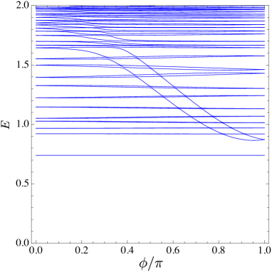
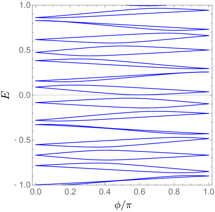
Based on the observations so far established in the light of the surface effective theory, let us re-examine the spectral flow shown in the four panels of Fig. 2 in more detail. Panels (a), (c) show a calculated spectral flow in the case of odd (), while panels (b), (d) correspond to the case of even (). Panels (a), (b) represent a spectral flow in the clean limit, while (c), (d) are those of the disordered case: . Model parameters are set as and (measured in units of ).
III.3.1 Case of odd: extended, perfectly conducting
Let us first focus on Fig. 2 (a): case of in the clean limit. In the range of energies shown in the figure, the low-lying part of three sub-bands with and of Eq. (8), are relevant, contributing to the spectral flow. The sub-band is non-degenerate and gapless, which is responsible for the non-trivialness of the flow. In the sector, the bottom of the degenerate sub-bands are located at
| (19) |
The simple zigzag pattern below this threshold energy is purely due to the sub-band, while above this energy the two contributions are superposed.
In the pure regime the pitch of the zigzag pattern is given as
| (20) |
[see Eq. (15)]. In the presence of disorder [Fig. 2 (c)] this pitch is modified by the mixing of and sub-bands, while the connectedness of the zigzag pattern is maintained; the spectral flow remains non-trivial. Crossing of the spectra at and is a consequence of the time reversal symmetry (Kramers degeneracy), which is unaffected by introduction of non-magnetic impurities considered here. Robustness of the continuous zigzag pattern is a clear signature that a pair of surface helical channels are robust against disorder, and the corresponding wave function is extended despite the presence of disorder [Fig. 3 (a)].
III.3.2 Case of even: all the states get localized
If is even, the situation is much different. First, the spectrum is gapped by a finite-size quantization [see Eq. (10)]. The half width of this gap is in the present choice of parameters [cf. Fig. 2, panel (b)]. Above this threshold energy, two pseudo degenerate sub-bands with become available for edge/surface conduction. In the clean limit [panel (b)] these two sub-bands form a zigzag pattern somewhat resembling the case of odd. Note that the two sub-bands are not completely degenerate; they interfere due to the existence of corners, and as a result their spectrum repel each other. Also importantly, there is a crossing once per each period between these pseudo degenerate sub-bands at a (non-protected) intermediate value of (recall the arguments in the previous subsection). Crossings occur with a counter-propagating partner, and between neighboring modes [see Eq. (12)].
Now, as we switch on disorder [see panel (d)], a crucial difference arises from the case of odd [panels (c)]. The zigzag is broken apart into many pieces; the spectral flow is indeed trivial in this case. In Fig. 3 (b) the spatial profile of the corresponding wave function is shown. In consistency with the trivial spectral flow the wave function is localized in the vicinity of one corner of the prism.
(a)
 (b)
(b)
III.4 Bound states
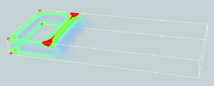
In the spectral flow shown in the four panels of Fig. 2, one can recognize a separate branch that are superposed on top of the spectral flow we have so far focused on. This separate branch stems from a bound state induced by the flux insertion. Imura et al. (2011a, b); Ran et al. (2009) This can be verified explicitly by inspecting the spatial profile of the corresponding wave function as shown in Fig. 3 (c), (d). The figure indicates that such bound states are localized around a plaquette through which the flux is inserted. That is, they can be regarded as localized states on the surface of a prism-shaped hole (i.e. flux tube) corresponding to the plaquette, where the circumference of the hole is with being the lattice constant. The reason why such bound states appear in the spectrum can be read from Eq. (15), while here the typical length scale is associated with the quantization of [see Eq. (12)]. As is chosen to be unity in the simulation, . The fact that is on the order of implies that -quantization and -quantization are equally important. This is contrasting to the case of surface states on side surfaces, in which holds, indicating that the -quantization is much more important. In the low-energy regime shown in Fig. 2 only the (or on the side) sector is relevant.
When is odd, -quantization allows for a zero mode: in Eq. (7). The separate branch that appears in the spectral flow shown in Fig. 2 (a), (c), and the spatial profile of the wave function shown in Fig. 3 (c) are due to such a bound state with and . Since
| (21) |
the energy of this bound state is zero at . Taking into account, one can also estimate the rough energy “dispersion” of this bound state from Eq. (15) as
| (22) |
In the spectral flow shown in Fig. 2 (a), (c), the separate branch due to bound state shows indeed such a linear dispersion in the vicinity of the gap closing at . In the high energy part of the spectral flow in the clean limit [Fig. 2 (a)], one can also recognize the second sets of bound states, which are due to and .
When is even, -quantization has no zero mode. The separate branch that can be seen in Fig. 2 (b), (d) are due to bound states with and . The spatial profile of the wave function in this case is shown in Fig. 3 (d). From Eq. (15) one can make a rough estimate of for such gapped bound states:
| (23) |
where in the present case with , i.e.,
| (24) |
Setting , one can apply Eq. (23) to the second excited bound states in the case of ,
| (25) |
Though such estimates as given in Eqs. (22), (23), (24), (25) are very rough ones, they still show a qualitatively good agreement with the calculated spectral flow presented as four panels in Fig. 2.
(a)
 (b)
(b)
IV Perfectly conducting channels emergent in WTI nano-architectures
Let us consider the step geometries as depicted in Fig. 1 (b), (c). A PCC appears along a step (or steps) etched on the surface of a WTI. In the case of a single step, the width of an otherwise uniform nano-flake differs on the two sides of the step simply by the height of the step, which we assume to be odd. Then, the height of the two sides is either odd-even, or even-odd. A PCC appears naturally on the side the width of which is odd, and is smoothly connected to the PCC along the step, forming a closed nano-circuit of PCC. We probe the nature of such PCC along the step and around the side surfaces by studying response of the system to flux and introduced on either side of the step, independently.
In the case of the double step [see panel (c) of Fig. 1], provided that the height of two steps is both odd, there are two possible options for the width of nano-flake on the two sides of the step. The height of the two sides is either odd-odd or even-even. In the case of the even-even combination there appears no PCC circulating around the nano-flake, so that two PCCs in the step region connect with each other, forming a single closed loop. This means that this combination reduces to the previous case of a single nano-circuit. The odd-odd combination realizes a typical example of multiple nano-circuit we intend to highlight in part B of this section.
IV.1 Case of the single step: a robust perfectly conducting channel running along the step
The model geometries depicted in Fig. 1 (b), (c) can be regarded as a set of two rectangular prisms of different height, say, and joined together via side surfaces. The gapped surfaces are on the top and bottom surfaces. Here, we align them such that the bottom surfaces are smoothly connected (case of the single step). Then, if , a step of height appears on the top surface. If is odd, there appears a pair of 1D protected helical modes (i.e., PCCs) along the step,Yoshimura et al. (2013) while if is even, this is no longer the case; pseudo 1D modes are gapped out by the finite size effect and do not appear in the low energy spectrum. Indeed, this odd/even feature with respect to stems from the difference of spectrum in the two cases [see Eq.(8)].
Let us consider a situation in which is odd and is even, say, and . Since is odd (), there appears a pair of 1D protected modes along the step. Yoshimura et al. (2013) Here, one can apply the same arguments leading to Eq. (8) for surface states emergent at the step. Naturally, these 1D helical modes cannot be confined in a finite segment of the step. They must be extended over to side surfaces of the prism. Surface states on such side surfaces become gapless [i.e., excepting the -discretization due to Eq. (12)] when is odd [case of Eqs. (8) with ]. In the situation we consider, this happens on the -side [Fig. 1 (b)]. Thus, in the region of but below the bottom of the surface sub-band on the -side located at the energy given by Eq. (10), the 1D modes along the step form a closed loop solely with the pseudo 2D surface modes on the -side [see Fig. 4 (c)]. Above this threshold energy (i.e., the bottom of the sub-band on the -side) an electron propagating via a 1D channel along the step and incident at a quantum junction that appears at the end of the step can turn either to the - or to the -side [see Fig. 4 (d)]. At energies above the bottom of second sub-band on the -side, given by Eq. (19), there seem to be a priori three, two and one pair of channels, incident, respectively, from the -, - and the step sides to the quantum junction.
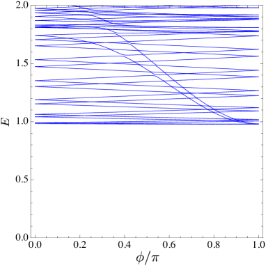
In the presence of disorder, however, not all of these channels survive. To see the robustness of different channels against disorder, here, we have studied the spectral flow in the system under insertion of a magnetic flux in two different configurations. In Figs. 4 and 5 such a spectral flow is presented in panel (a) under a flux configuration of , where and represent, respectively, a flux inserted on the -side and on the -side. In panel (b) of Figs. 4 and 5 a different configuration of is studied. Two panels of Fig. 4 represent a spectral flow in the clean limit (), while a moderate strength of disorder () is introduced in the examples shown in Fig. 5. As one can clearly see in Fig. 5 a nontrivial spectral flow is still persistent in panel (a), i.e., the spectral flow is non-trivial in this case, while the flux dependence is almost extinct in panel (b); the spectral flow is trivial in this case. This indicates that in the single step geometry as depicted in Fig. 1 (b) with odd (), even () [and therefore, odd ()], an electron in the 1D protected channel at the step is selectively transmitted to the -side in the presence of disorder: .
(a)
 (b)
(b)
IV.2 Two step geometry: an even number of channels running in parallel
In the previous examples, only surfaces consisting of an odd number of channels are robust against disorder, and such surfaces occur when the layer number is odd. A natural question that arises here is what happens in a geometry as depicted in Fig. 1 (c) if , , , are all odd? We consider typically the case of and with and .
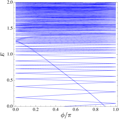
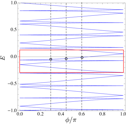
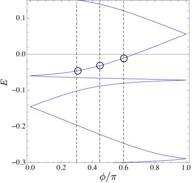
Fig. 6 shows response of such a system against flux insertion both on the - and -sides [see configuration of the two types of flux insertion and in Fig. 1 (b)]. The two panels of Fig. 6 show evolution of the spectrum at as a function of the flux when the flux is inserted either on the - or on the -side; in panel (a), and in panel (b).
We begin by pointing out two specific features that can be seen in the two panels of Fig. 6. First, both panels show a non-trivial spectral flow, in which each member of a Kramers pair at changes its partner at . This means that there exists a robust perfectly conducting channel both around the prism 1 and around the prism 2. Provided that and are both odd (), one expects a priori an even number () of channels running in parallel at the connection of two prisms. Yet, the obtained spectral flow implies that the two channels behave as if there were an odd number of channels. We will clarify this point later. Secondly, the two spectra are complementary in the sense that those partners that are sensitive to are insensitive to , and vice versa. Note that at the two plots coincide, since the two simulation is done for the same configuration of impurities.
Those states that are sensitive to the flux in Fig. 6 (a) stem from states that goes around the prism 1 [1c and 1a modes in Fig. 7, panel (b)], while those which are insensitive to the flux are states that goes around the prism 2 (2c and 2a, ibid.). To check these assumptions, here, we have designed the system such that the circumference of 2c and 2a modes is twice as long as that of 1c and 1a (): . Note that separation of the levels associated with a 1D channel due to finite size is inversely proportional to its circumference. In panel (a) those pairs that are sensitive to the flux are spaced by a distance twice as large as those which are insensitive to the flux. Since the former is assumed to stem from 1c and 1a, while the latter from 2c and 2a, this makes perfectly sense.
These being said, let us come back to the question: why are the even number of channels incident at the steps robust against disorder? Why do they behave like an odd number of channels, showing a nontrivial spectral flow? Our short answer is the following: if we focus on some energy , say, in the spectrum shown in Fig. 6 (a), there exists indeed an odd number of (here, only one) channel(s) at the step. To elaborate what this actually implies, let us divide the spectrum in energy into two types of pieces. The first type of pieces are sensitive to the flux , while the remaining pieces are insensitive. The first type of pieces are due to states which in real space distributed predominantly in prism 1, while the remaining part of the spectrum is due to states stemming from prism 2. As varying , one can evolve a state incident mainly in prism 1, into a state extended over to the side of prism 2 [see Fig. 8], but then the energy is changed. Or, conversely, if an energy is given, there exists a certain value of at which an eigenstate of the system is available. Then at this energy, the spatial profile of the available electronic state is uniquely determined. When energy is varied, both electronic states in prism 1 and the ones in prism 2 become available, but never at the same energy. As a result, the spectral flow “segregates” into two regions. The two regions do not coexist, but are connected smoothly. At a given energy , there exists only a single state (at some value of ) either on the - or on the -side (or sometimes in between). This serves as the “traffic rule” applied here to the T-junctions at both ends of the step. The signal at the T-junction permits either a left or a right turn depending on the energy of the incident electron.
(a)
 (b)
(b)
 (c)
(c)
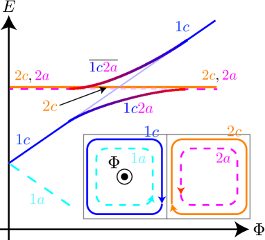
Let us try to formulate how this segregation occurs by zooming up a part of the spectral flow shown in the red frame of Fig. 6 (a). Fig. 7 (a) shows an enlarged image of this part of the flow. Those parts of the spectrum that are sensitive to the flux are due to states circulating the prism 1 either in the clockwise or in the anti-clockwise direction [1c and 1a modes in Fig. 7 (b)]. On contrary, those parts of the spectrum that are insensitive to the flux are due to states circulating the prism 2 (2c and 2a modes). However, in the presence of the step region at which two prisms are coupled, the eigenstates of the system become a combination of 1c/1a and 2c/2a states; they are mixed and recombined in the step region. In Fig. 7 (a) two Kramers pairs, 1c/1a and 2c/2a, are incident at apart in energy. Here, we consider the spectral flow of the system under a flux inserted in the configuration of . As () is increased, 1c/1a pair breaks; is the upward branch, which intersects with the 2c/2a pair located initially above. As schematically illustrated in panel (b), the spectral feature in the vicinity of this intersection can be understood as the result of anti-crossing between and, intrinsically, a linear combination of and . Since the spin quantization axis of the two helical pairs: 1c/1a and 2c/2a, are not not necessarily aligned, one expects a priori recombination of such modes at the step region. In principle, is coupled to either or , or to both. Let us introduce the linear combination:
| (26) |
where and are some constants normalized such that , and assume that is coupled to at the step region. Then, this signifies that is orthogonal to , and represents a branch that is unaffected by the proximity to . Indeed, state remains flat, insensitive to the flux, and there is no anti-crossing between and . Only at it reunites with . In contrast to the flat -subband, and show a clear anti-crossing feature. The two branches of the anti-crossing may be presented as
| (27) |
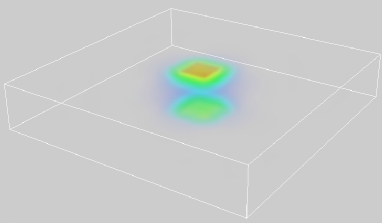
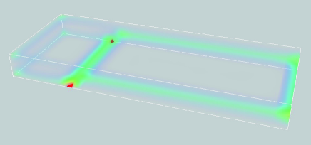
where and are some constants that vary as a function of : and . The constants and are also normalized such that . Let us assume that represents the bonding branch focused in Fig. 7 (a) and (b), while corresponds to the anti-bonding branch. To illustrate the evolution of as a function of , we have plotted in Fig. 8, the spatial profile of the corresponding wave function at different values of (). One can see that a dominant weight of the wave function is on the -side at , which is shifted to the -side as is increased.
(a)
(b)
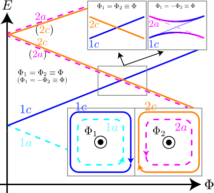
In Eq. (26) we assumed simply that is coupled to the -combination, without actually specifying what a percentage comes from in this combination, and what a percentage from . In this last part, we clarify this point by studying yet another type of spectral flow. Two panels of Fig. 9 show such a spectral flow in the cases of flux configurations such that in panel (a), i.e., case of the flux introduced in the same direction on the and sides, while in panel (b), i.e., case of the flux inserted in the opposite directions. Whether the spectrum responds either in the upward or downward direction is a combined effect of the direction of the propagating 1D channel and that of the flux introduced. Therefore, by changing the relative sign of with respect to , one can bring together different combinations of channels in the flow of the spectrum (see Fig. 10).
For example, in the -configuration, combinations such as (1c, 2a) and (2c, 1a), i.e., pairs of co-propagating modes, get close to one another in the spectral flow. As one can see in Fig. 9 (a), the two branches show clear anti-crossing, making the flow of the spectrum disconnected. These co-propagating pairs indeed couple and recombine at the step region. On contrary, in the -configuration [Fig. 9 (b)], combinations such as (1c, 2c) and (1a, 2a), i.e., a pair of counter-propagating modes, meet in the spectral flow, and show practically no conspicuous anti-crossing. These imply that at the step region the co-propagating combinations such as (1c, 2a) and (2c, 1a) are coupled, while counter-propagating combinations such as (1c, 2c) and (1a, 2a) are not coupled, i.e., , in terms of Eq. (26), implying actually . The co-propagating combinations compose the -dependent part, while the counter-propagating combinations are responsible for the -independent part, i.e., the flat part of the spectral flow shown in Figs. 6 and 7, ensuring together the connectedness of the nontrivial spectral flow.
In the situation studied so far we have seen that the entire circuit is no longer perfectly conducting as a result of the coupling between multiple channels. Yet, there still exists a perfectly conducting channel in the network, which is now nontrivially distributed in space, extended over coupled circuits (see Fig. 8). A prominent feature also manifests in the energy-momentum space as a specific type of continuous spectral flow (Fig. 7).
V concluding remarks
We have studied protected helical conducting channels that appear in WTI nano-flakes, WTI terraces, and WTI nanoarchitectures, and their robustness against disorder. After a close inspection of the nano-flake case in Sec. III, we have highlighted the cases of WTI terraces and steps in Sec. IV. In contrast to the case of a single step, an electron incident at the step region in the two-step geometry can be transmitted to either side of the step. To study the nature of the corresponding spectral flow, encoding the robustness or non-robustness of the helical channel, was one of the central issues addressed in the paper. In the geometry studied an even number of helical channels are incident at the step region, which can, in principle, be gapped out and get localized in the presence of disorder. Yet, we find a nontrivial, connected spectral flow as a clear signature of the immunity to disorder. This happens in such a way that each part of the spectrum corresponding to a different 1D channel appear in segregated energy regions, but as a whole the spectral flow is connected, i.e., each piece of the spectrum in a segregated energy region combines to give the entire connected spectrum. As a result, these even number of channels are protected and robust against disorder, alike the case of an odd number of channels. At a quantum junction at each end of the step region a non-trivial, energy dependent “traffic rule” emerges.
In nano-circuits fabricated on surfaces of a WTI, a number of 1D channels appear, meet and couple in a nontrivial manner, forming nontrivial quantum junctions at which more than two channels meet in a nontrivial manner. Ilan et al. (2014) Here, we have shown an example in which incident 1D channels stay extended in spite of such coupling. The obtained results indicate that robustness of the 1D helical channels established in simple nano-structures, such as WTI nano-flakes and steps, is a generic feature that can be applied to more involved and realistic nanoarchitectures.
Acknowledgements.
Y.Y. is supported by JSPS as a Special Doctoral Researcher and by Grant No. 15J06436. Y.T. and K.I. are supported by a Grant-in-Aid for Scientific Research (B) and (C) (Nos. 24540375, 15H0370001, 15K05130 and 15K05131).Appendix A Derivation of Eqs. (5), (7), (8)
The low-enery electron states that appear on the side surface of are described by the following effective Hamiltonian:Arita and Takane (2014)
| (33) | |||||
where represents two-component state vector for the th 1D helical channel, and represents a component of the momentum in the direction the side surface is extended, say, or .
Eq.(33) exhibits two Dirac cones centered at and in the reciprocal space. The wave function for a surface state with is expressed as
| (36) |
where or . In the expression Eq. (36)
| (41) |
where the transverse function must satisfy the boundary condition of
| (42) |
By superposing plane wave solutions stemming from two Dirac cones: , , one can construct a wave function compatible with Eqs. (41) and (42) such that
| (47) | |||||
| (50) |
where satisfies
| (51) |
From Eq. (51), one finds
| (52) |
Allowed discrete values of given in Eq. (7) are specified by the second equality of Eq. (42) by the vanishing of at , i.e.
| (53) |
where is either an integer or a half-odd integer. For an odd , takes an integral value; . While for even, becomes a half-odd integer; . Substituting Eq. (53) into Eq. (52), one completes the derivation of Eqs. (5) and (8).
References
- Moore and Balents (2007) J. E. Moore and L. Balents, Phys. Rev. B 75, 121306 (2007), URL http://link.aps.org/doi/10.1103/PhysRevB.75.121306.
- Fu et al. (2007) L. Fu, C. L. Kane, and E. J. Mele, Phys. Rev. Lett. 98, 106803 (2007), URL http://link.aps.org/doi/10.1103/PhysRevLett.98.106803.
- Roy (2009) R. Roy, Phys. Rev. B 79, 195322 (2009), URL http://link.aps.org/doi/10.1103/PhysRevB.79.195322.
- Nomura et al. (2007) K. Nomura, M. Koshino, and S. Ryu, Phys. Rev. Lett. 99, 146806 (2007), URL http://link.aps.org/doi/10.1103/PhysRevLett.99.146806.
- Bardarson et al. (2007) J. H. Bardarson, J. Tworzydlo, P. W. Brouwer, and C. W. J. Beenakker, Phys. Rev. Lett. 99, 106801 (2007), URL http://link.aps.org/doi/10.1103/PhysRevLett.99.106801.
- Takane and Imura (2012) Y. Takane and K.-I. Imura, Journal of the Physical Society of Japan 81, 093705 (2012), eprint http://dx.doi.org/10.1143/JPSJ.81.093705, URL http://dx.doi.org/10.1143/JPSJ.81.093705.
- Ran et al. (2009) Y. Ran, Y. Zhang, and A. Vishwanath, Nature Physics 5, 298 (2009).
- Imura et al. (2011a) K.-I. Imura, Y. Takane, and A. Tanaka, Phys. Rev. B 84, 035443 (2011a), URL http://link.aps.org/doi/10.1103/PhysRevB.84.035443.
- Ringel et al. (2012) Z. Ringel, Y. E. Kraus, and A. Stern, Phys. Rev. B 86, 045102 (2012), URL http://link.aps.org/doi/10.1103/PhysRevB.86.045102.
- Liu et al. (2012) C.-X. Liu, X.-L. Qi, and S.-C. Zhang, Physica E Low-Dimensional Systems and Nanostructures 44, 906 (2012), eprint 1110.3420.
- Imura et al. (2012) K.-I. Imura, M. Okamoto, Y. Yoshimura, Y. Takane, and T. Ohtsuki, Phys. Rev. B 86, 245436 (2012), URL http://link.aps.org/doi/10.1103/PhysRevB.86.245436.
- Yoshimura et al. (2013) Y. Yoshimura, A. Matsumoto, Y. Takane, and K.-I. Imura, Phys. Rev. B 88, 045408 (2013), URL http://link.aps.org/doi/10.1103/PhysRevB.88.045408.
- Takane (2014) Y. Takane, Journal of the Physical Society of Japan 83, 103706 (2014), eprint http://dx.doi.org/10.7566/JPSJ.83.103706, URL http://dx.doi.org/10.7566/JPSJ.83.103706.
- Kobayashi et al. (2014) K. Kobayashi, K.-I. Imura, Y. Yoshimura, and T. Ohtsuki, ArXiv e-prints (2014), eprint 1409.1707.
- Rasche et al. (2013) B. Rasche, A. Isaeva, M. Ruck, S. Borisenko, V. Zabolotnyy, B. Buechner, K. Koepernik, C. Ortix, M. Richter, and J. van den Brink, Nature materials 12, 422 (2013).
- Pauly et al. (2015) C. Pauly, B. Rasche, K. Koepernik, M. Liebmann, M. Pratzer, M. Richter, J. Kellner, M. Eschbach, B. Kaufmann, L. Plucinski, et al., Nat Phys 11, 338 (2015), URL http://dx.doi.org/10.1038/nphys3264.
- Ando (2013) Y. Ando, Journal of the Physical Society of Japan 82, 102001 (2013), eprint http://journals.jps.jp/doi/pdf/10.7566/JPSJ.82.102001, URL http://journals.jps.jp/doi/abs/10.7566/JPSJ.82.102001.
- Bahramy et al. (2012) M. Bahramy, B.-J. Yang, R. Arita, and N. Nagaosa, Nature communications 3, 679 (2012).
- Yan et al. (2012) B. Yan, L. Muechler, and C. Felser, Phys. Rev. Lett. 109, 116406 (2012), URL http://link.aps.org/doi/10.1103/PhysRevLett.109.116406.
- Fukui et al. (2013) T. Fukui, K.-I. Imura, and Y. Hatsugai, Journal of the Physical Society of Japan 82, 073708 (2013), eprint http://journals.jps.jp/doi/pdf/10.7566/JPSJ.82.073708, URL http://journals.jps.jp/doi/abs/10.7566/JPSJ.82.073708.
- Yang et al. (2014) G. Yang, J. Liu, L. Fu, W. Duan, and C. Liu, Phys. Rev. B 89, 085312 (2014), URL http://link.aps.org/doi/10.1103/PhysRevB.89.085312.
- Yoshimura et al. (2014) Y. Yoshimura, K.-I. Imura, T. Fukui, and Y. Hatsugai, Phys. Rev. B 90, 155443 (2014), URL http://link.aps.org/doi/10.1103/PhysRevB.90.155443.
- Fu (2011) L. Fu, Phys. Rev. Lett. 106, 106802 (2011), URL http://link.aps.org/doi/10.1103/PhysRevLett.106.106802.
- Hsieh et al. (2012) T. H. Hsieh, H. Lin, J. Liu, W. Duan, A. Bansil, and L. Fu, Nature Communications 3, 982 (2012), URL http://www.nature.com/ncomms/journal/v3/n7/full/ncomms1969.html.
- Tanaka et al. (2012) Y. Tanaka, Z. Ren, T. Sato, K. Nakayama, S. Souma, T. Takahashi, K. Segawa, and Y. Ando, Nature Physics 8, 800 (2012), URL http://www.nature.com/nphys/journal/v8/n11/abs/nphys2442.html.
- Dziawa et al. (2012) P. Dziawa, B. Kowalski, K. Dybko, R. Buczko, A. Szczerbakow, M. Szot, E. Lusakowska, T. Balasubramanian, B. M. Wojek, M. Berntsen, et al., Nature Materials 11, 1023 (2012), URL http://www.nature.com/nmat/journal/v11/n12/full/nmat3449.html.
- Morimoto and Furusaki (2013) T. Morimoto and A. Furusaki, Phys. Rev. B 88, 125129 (2013), URL http://link.aps.org/doi/10.1103/PhysRevB.88.125129.
- Kane and Mele (2005) C. L. Kane and E. J. Mele, Phys. Rev. Lett. 95, 146802 (2005), URL http://link.aps.org/doi/10.1103/PhysRevLett.95.146802.
- Takane (2004) Y. Takane, Journal of the Physical Society of Japan 73, 1430 (2004), URL http://jpsj.ipap.jp/link?JPSJ/73/1430/.
- Zhang et al. (2010) H. Zhang, C.-X. Liu, X.-L. Qi, X. Dai, Z. Fang, and S.-C. Zhang, Nature Physics 5, 438 (2010).
- Liu et al. (2010) C.-X. Liu, X.-L. Qi, H. Zhang, X. Dai, Z. Fang, and S.-C. Zhang, Phys. Rev. B 82, 045122 (2010).
- Kobayashi et al. (2013) K. Kobayashi, T. Ohtsuki, and K.-I. Imura, Phys. Rev. Lett. 110, 236803 (2013), URL http://link.aps.org/doi/10.1103/PhysRevLett.110.236803.
- Sbierski and Brouwer (2014) B. Sbierski and P. W. Brouwer, Phys. Rev. B 89, 155311 (2014), URL http://link.aps.org/doi/10.1103/PhysRevB.89.155311.
- Buettiker et al. (1983) M. Buettiker, Y. Imry, and R. Landauer, Physics Letters A 96, 365 (1983), ISSN 0375-9601, URL http://www.sciencedirect.com/science/article/pii/0375960183900117.
- Mong et al. (2012) R. S. K. Mong, J. H. Bardarson, and J. E. Moore, Phys. Rev. Lett. 108, 076804 (2012), URL http://link.aps.org/doi/10.1103/PhysRevLett.108.076804.
- Fu and Kane (2012) L. Fu and C. L. Kane, Phys. Rev. Lett. 109, 246605 (2012), URL http://link.aps.org/doi/10.1103/PhysRevLett.109.246605.
- Obuse et al. (2014) H. Obuse, S. Ryu, A. Furusaki, and C. Mudry, Phys. Rev. B 89, 155315 (2014), URL http://link.aps.org/doi/10.1103/PhysRevB.89.155315.
- Arita and Takane (2014) T. Arita and Y. Takane, Journal of the Physical Society of Japan 83, 124716 (2014), eprint http://dx.doi.org/10.7566/JPSJ.83.124716, URL http://dx.doi.org/10.7566/JPSJ.83.124716.
- Zhang et al. (2009) Y. Zhang, Y. Ran, and A. Vishwanath, Phys. Rev. B 79, 245331 (2009), URL http://link.aps.org/doi/10.1103/PhysRevB.79.245331.
- Zhang and Vishwanath (2010) Y. Zhang and A. Vishwanath, Phys. Rev. Lett. 105, 206601 (2010), URL http://link.aps.org/doi/10.1103/PhysRevLett.105.206601.
- Bardarson et al. (2010) J. H. Bardarson, P. W. Brouwer, and J. E. Moore, Phys. Rev. Lett. 105, 156803 (2010), URL http://link.aps.org/doi/10.1103/PhysRevLett.105.156803.
- Ostrovsky et al. (2010) P. M. Ostrovsky, I. V. Gornyi, and A. D. Mirlin, Phys. Rev. Lett. 105, 036803 (2010), URL http://link.aps.org/doi/10.1103/PhysRevLett.105.036803.
- Imura et al. (2011b) K.-I. Imura, Y. Takane, and A. Tanaka, Phys. Rev. B 84, 195406 (2011b), URL http://link.aps.org/doi/10.1103/PhysRevB.84.195406.
- Ilan et al. (2014) R. Ilan, F. de Juan, and J. E. Moore, ArXiv e-prints (2014), eprint 1410.5823.