Stacking sequence dependence of electronic properties in double-layer graphene heterostructures
Abstract
First-principles calculation has been performed to investigate the stability and electronic properties of double-layer graphene heterostructure (DLGH). In this system, two graphene layers are separated by hexagonal boron-nitride (h-BN) layers which work as a insulating barrier. Our results show that the stability of the system is determined by the atomistic configurations between graphene and its adjacent h-BN layer. Among different stacking sequences, Ab-stacking is most stable. Since the inserted h-BN layers modulate the on-site energies for carbon atoms of graphene layers, the electronic states of the system can be classified into metallic or semiconducting by the stacking sequence. And the stacking sequence dependence of the energy band structures of DLGHs are well described by the orbital interaction model.
1 Introduction
Monolayer graphene invokes great interest in electronic application owing to the unique properties such as ultra-high electronic mobility, anomalous quantum Hall effects and so on. [1, 2, 3, 4, 5, 6, 7] These unconventional electronic properties are originated from the unusual band structure near the Fermi level of graphene, where the electronic states are well described as massless Dirac electrons, i.e. a zero energy gap with linear bands crossing at the point. In few-layer graphene system, however, the weak interaction between graphene layers changes the electronic properties near the Fermi level. [8, 9, 10, 11, 12] For bilayer graphene, Bernal AB-stacking graphene which is more stable than AA-stacking one shows a metallic behavior with chiral parabolic dispersions near the point. For trilayer graphene, there are two kinds of stacking sequences, i.e. Bernal AB and rhombohedral ABC stacking. Though both of them are semi-metallic, the detailed band structures differ depending on the stacking sequence. Accordingly, their electronic properties under external electric fields and the optical conductivity depend on the stacking sequence. [8, 13] Thus, even if the interlayer interaction is weak, the stacking structures are crucial in determining the electronic properties of the layered materials.
Recently, double-layer graphene heterostructures (DLGHs), in which hexagonal boron-nitride (h-BN) layers are inserted between two graphene layers, are investigated and exhibit many interesting properties such as tunable metal-insulator transition, good room-temperature switching ratios, strong coulomb drag and so on. [14, 15, 16, 17, 18, 19, 20] In these experiments, h-BN layers are used as a tunnel barrier with varying thickness from one to dozens of layers. It is shown that the tunneling resistance of the heterostructure is sufficiently high for the h-BN spacer of three atomic layers, and becomes unacceptable low for bilayer h-BN. [16, 21, 22] In these DLGHs, where the number of h-BN layers is one, two and three, the interlayer interaction between graphene and its adjacent h-BN layer influences on the electronic properties of the graphene. In addition, owing to the short distance between graphene layers, the interlayer interaction between two graphene layers is still not negligible similar to tri- and tetra-layer graphenes. Therefore, the electronic properties of DLGHs are different from mono- and bi-layer graphenes on a h-BN substrate. To clarify this difference in electronic properties, in this paper we investigate the electronic structures of DLGHs on the basis of density functional theory. We discuss the stability and energy band structure of the DLGHs by changing the number of h-BN layers and the stacking sequence. Our results show that the coupling between graphene layer and its adjacent h-BN layer becomes most stable with Ab-stacking sequence. It is also shown that the electronic states of DLGHs can be classified into metallic or semiconducting by the stacking sequence. The simple orbital interaction model qualitatively well describe the stacking sequence dependence of the energy band structures of DLGHs.
2 Calculation Method and Simulation Model
The calculations are performed using density functional theory based Vienna Ab initio Simulation Package (VASP). [23] Core and valence electrons are described with the projector-augmented wave method (PAW). [24] The local density approximation (LDA) is used to treat the exchange-correlation functional.[25] The plane-wave basis set cutoff is 500 eV and the Brillouin zone is sampled with 13131 Monkhorst-Pack mesh. The DLGHs investigated in this paper have the sandwiched structures; h-BN layers are inserted as the spacer between two graphene monolayers. We label the system as G-BN-G. The number of h-BN layers is changed from one to three. As the lattice mismatch between graphene and h-BN monolayer is around 1.8%, the graphene and h-BN layers can be assumed to be commensurate. To ensure negligible interaction between periodic images of the slabs in the stacking direction, 20Å vacuum is used. In this study, all the structures are fully optimized including atomic coordinates and supercell. The convergence thresholds for energy and force are 10-4eV and 0.01eV/Å.
3 Results and Discussions
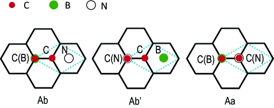
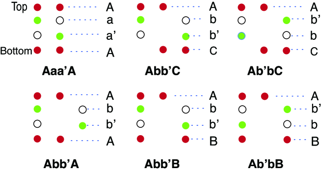
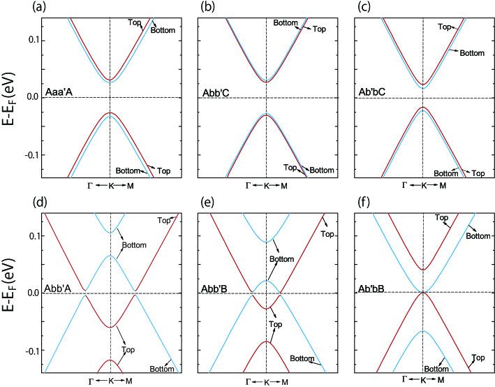
In this work, the stacking sequences are distinguished using the naming convention defined in the paper of Sakai et al. [26, 27] The capital letters (A, B, C) and small letters (a, b, c) represent the relative stacking positions of graphene and h-BN layer, respectively. For example, the Bernal stacking sequence of bilayer graphene is labeled as AB, and the stacking form of bulk h-BN is aa′. The prime symbol represents exchange of the positions of boron and nitrogen atoms in the adjacent h-BN layers. Figure 1 shows three nonequivalent orientations of graphene on h-BN monolayer (Ab, Ab′ and Aa). Since h-BN layers always have an aa′ stacking, a DLGH can have six different stacking sequences with a fixed thickness. Figure 2 shows the six different stacking configurations of G-2BN-G. The corresponding energy band structures are shown in Fig.3.
Let us try to find out the most stable stacking sequence of DLGHs. In order to clarify the relative stability among different stacking sequences for a fixed thickness, we have evaluated the relative differences of the total energy E for each stacking configuration shown in Table Stacking sequence dependence of electronic properties in double-layer graphene heterostructures . E is defined as the energy difference of the total energy for each configuration measured from that of the most stable structure for a fixed thickness of DLGH. We can see that the most stable structure in each thickness group favor Ab-stacking between graphene and its adjacent h-BN layer except G-2BN-G. Ab-stacking sequence is that the carbon atoms on one of two sublattices are above boron atoms and carbon atoms on the other sublattice are above the centers of the BN hexagonal rings. According to this definition, b′C-stacking is equivalent to bA-stacking. Therefore, the most stable configuration in G-2BN-G is Abb′C, where both layers of graphene are also Ab-stacking with their adjacent h-BN layers. The DLGHs with Aa or Aa′ stacking sequence, which are least stable, have 40meV higher total energy than that of the most stable structure.
The stability of DLGHs can also be embodied by the interlayer distance between graphene and its adjacent h-BN layer. We find that the average interlayer distances between the graphene and the h-BN layer are 3.24Å for Ab-stacking, 3.46Å for Ab′-stacking and 3.52Å for Aa-stacking, respectively. This fact means that the shorter interlayer distance gives the larger stability of DLGHs due to the stronger interaction. Since Ab-stacking is most stable, the interaction between boron and carbon atoms is favorable. This fact is consistent with the results of the graphene/h-BN bilayer superlattices. [26, 27]
The energy band gaps of G-BN-G are shown in Table Stacking sequence dependence of electronic properties in double-layer graphene heterostructures . First, we discuss the band structures of G-2BN-G and G-3BN-G. In these two cases, the band gaps can be classified into two types: (1) larger band gaps of dozens of meV and (2) very tiny band gaps of less than 10meV. To clarify the mechanism of two types of the band gaps, we investigate the effect of interlayer interaction and stacking sequence on the band structures of heterostructures. In the DLGHs, the two graphene layers are separated by h-BN layers, therefore graphene interacts with h-BN directly. Previous studies showed that this interaction causes the difference of on-site energies for carbon atoms between two sublattices, which induces a small band gap of dozens of meV. [28, 29, 30] Since G-1BN-G has much stronger interlayer interaction between graphenes than other cases, its electronic band structure will be discussed later.
In addition to the interlayer interaction, the stacking sequences crucially affect the electronic states near the Fermi energy. Let us consider the configuration Abb′A as an example (see Fig. 2). The corresponding energy band structure is shown in Fig. 3(d). As for the top (bottom) graphene layer, the carbon atoms on two different sublattices are located above (below) the boron (nitrogen) atoms and the centers of hexagonal h-BN rings, respectively. Therefore, the electrostatic potential of the top and bottom graphene layers in Abb′A heterostructure is different. In accordance with this fact, the energy dispersion related to the top (bottom) graphene layer shifts about 0.07 eV downward (upward) as can be seen in Fig. 3(d). On the contrary, for Abb′C, as the carbon atoms on two different sublattices in top (bottom) graphene layer are located above (under) the boron atoms and centers of h-BN hexagonal rings, both the layers of graphene have same electrostatic potential. Therefore, the energy dispersion related to the top and bottom graphene layers overlaps at almost same place as can be seen in Fig.3(b).
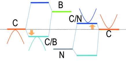
To understand the effect of different stacking sequences on energy band structure of DLGH, an orbital interaction model is employed. [31] Here we just consider the interaction between the orbitals of adjacent atoms. According to atom electronegativity, i.e. NCB, the energy levels of the orbitals of N, C, B atoms (EN, EC, EB) are EBECEN. In Fig.4, schematic energy diagram is shown to illustrate the shift of energy levels induced by the interaction between graphene and h-BN layer. For h-BN monolayer, at point, the top of valence band is mainly contributed by nitrogen atoms and the bottom of conduction band is contributed by boron atoms, respectively. Therefore, when the carbon atom is located above or below the boron atom, the occupied carbon orbital interacts with the empty boron orbital, leading to the downward shift of the bonding state from the original carbon level. As for the interaction between carbon and nitrogen atoms, the situation is opposite. The empty carbon orbital interacts with nitrogen orbital, resulting in the upward shift of energy level of anti-bonding state.
The shift of orbital energy for carbon atom can explain the band structures of DLGHs. In the case of tetralayer heterostructures, for Aaa′A, Abb′C, Ab′bC configurations, the top and bottom graphene layers have the same stacking sequence with their adjacent h-BN layers. Therefore, the interaction with the adjacent h-BN layers makes the carbon energy levels move in the same direction. In this situation, as shown in Figs.3(a)-(c), the energy band structures of those heterostructures are similar to that of graphene monolayer on h-BN layer. For another three heterostructures Abb′A, Abb′B and Ab′bB, the stacking of the top and bottom graphene layers with h-BN layers are in different ways, which induces the carbon orbital energies of two graphenes shift towards opposite directions, as shown in Figs.3(d)-(f). Let us take Abb′A as an example. The energy band corresponding to bottom graphene moves upwards and the energy band corresponding to top graphene moves downwards. Around the Fermi level, the energy bands from top and bottom graphenes intersect. At the crossing point, there are small openings of energy band gap. For Abb′A, it is 8meV and for Abb′B, it is 5meV. We attribute the band gap opening at the crossing points to the coupling of the top and bottom graphene layers mediated by h-BN layers. For penta layer heterostructures Abb′bB and Abb′bC where three layers of h-BN are inserted, the band structures are similar to that of Abb′A and Abb′B tetralayer heterostructures. However, the band gaps at the cross points are almost zero, which indicates the much weakened inter-graphene interaction.
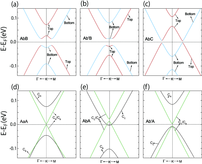
Figure 5 shows the energy band structures of G-1BN-G for six different stacking sequences. For G-1BN-G, the coupling between top and bottom graphene layers is stronger than that of G-2BN-G and G-3BN-G. As a result, the band structures near the Fermi level become more complex. For AbB, Ab′B and AbC configurations, their energy band structures become similar to those of Abb′bB, Ab′bb′B and Abb′bC, because of the similar stacking configuration between graphene and its adjacent h-BN layer. The only difference is that the interlayer distance between two graphenes is shorter in trilayer heterostructures, resulting in the larger band gaps owing to the stronger interlayer interaction. For AbA, Ab′A and AaA configurations, though the stacking sequences between graphene and h-BN are same as those of Abb′bA, Ab′bb′A and Aaa′aA, the band structures are totally different. As shown in Figs.5(d)-(f), there are two kinds of energy bands around the Fermi level. One energy band is approximately linear at point, and the other one is non-linear. We find that this linear energy band is contributed by all four carbon atoms in the unit cell, which is similar to the linear band state existing in ABA-stacking trilayer graphene.[8]. For ABA-stacking trilayer graphene, the linear band states are referred to be the bonding state of orbitals at both ends via the second neighbor hopping parameter . For AbA, Ab′A and AaA heterostructures, the situation is similar. Just the sandwiched layer is changed from graphene to h-BN, so the second neighbor hopping parameter is different. As for the nonlinear energy band, the energy levels of the carbon atoms with same electrostatic potential move towards same direction, because of which they compose one energy band, labeled as CB, CN and CC. This indicates that the coupling between top and bottom graphene plays a more important role.
From the above results, it is clear that the band structures can demonstrate the difference of the coupling of the two graphene layers. The coupling of the graphene layers is strong in trilayer heterostructures in spite of the existence of tunnel barrier of h-BN. As the number of h-BN layers increases, the coupling is weakened.
4 Conclusions
In this paper, first-principles calculation has been performed to investigate the stability and the energy band structure of DLGHs, where h-BN layers are inserted between two graphene monolayers. Our results show that the stability and band structures are sensitive to the stacking sequence of DLGHs. It is found that the stability of DLGHs is mainly dependent on the stacking sequence of graphene and its adjacent h-BN layer. Among the three stacking sequences, Ab-stacking is most stable. In addition, it is found that the interaction between graphene and h-BN affects the electronic properties in two aspects. First one is modification of on-site energy of carbon atoms between two nonequivalent sublattices in the same graphene. The second one is shifting the band structures of the top and bottom graphene layers, like graphene under an external electronic field. Our results give the fundamental aspects of the electronic states of DLGHs for the application of electronic devices.
K. W. acknowledges the financial support by Grant-in-Aid for Scientific Research from MEXT and JSPS (Nos. 25107005, 23310083 and 20001006).
References
- [1] K. S. Novoselov, A. K. Geim, S. V. Morozov, D. Jiang, M. I. Katsnelson, I. V. S. Grigorieva, V. Dubonos and A. A. Firsov, Nature 438, 197 (2005).
- [2] Y. B. Zhang, Y. W. Tan, H. L. Stormer and P. Kim, Nature 438, 201 (2005).
- [3] A. K. Geim, Science 324, 1530 (2009).
- [4] K. I. Bolotin, K. J. Sikes, Z. Jiang, M. Klima, G. Fudenberg, J. Hone, P. Kim and H. L. Stomer, Solid State Commun. 146, 351 (2008).
- [5] A. A. Balandin, S. Ghosh, W. Z. Bao, I. Calizo, D. Teweldebrhan, F. Miao, and C. N. Lau, Nano Lett. 8, 902 (2008).
- [6] T. Ando, J. Phys. Soc. Jpn. 74, 777 (2005).
- [7] F. Schweirz, Nat. Nanotechenol. 5, 487 (2010).
- [8] M. Aoki and H. Amawashi, Solid. State. Comm. 142, 123 (2007).
- [9] M. Klintenberg, S. Lebgue, C. Oritz, B. Sanyal, J. Fransson and O. Eriksson, J. Phys.: Condens. Matter 21, 335502 (2009).
- [10] J. A. Yan, W. Y. Ruan and M. Y. Chou, Phys. Rev. B 83, 245418 (2011).
- [11] F. Zhang, B. Sahu, H. Min, and A. H. MacDonald, Phys. Rev. B 82, 035409 (2010).
- [12] D. H. Xu, J. Yuan, Z. J. Yao, Y. Zhou and F. C. Zhang, Phys. Rev. B 86, 201404(R) (2012).
- [13] C. H. Lui, Z. Q. Li, K. F. Mak, E. Cappelluti and T. F. Heinz, Nature Phys. 7, 944 (2011).
- [14] L. Britnell, R. V. Gorbachev, R. Jalil, B. D. Belle, F. Schedin, A. Mishchenko, T. Georgiou, M. I. Katsnelson, L. Eaves, S. V. Morozov, N. M. R. peres, J. Leist, A. K. Geim, K. S. Novoselov and L. A. Ponomarenko, Science, 335, 947 (2012).
- [15] L. A. Ponomarenko, A. K. Geim, A. A. Zhukov, R. Jalil, S. V. Morozov, K. S. Novoselov, I. V. Grigorieva, E. H. Hill, V. V. Cheianov, V. I. Fal′ko, K. Watanabe, T. Taniguchi and R. V. Gorbachev, Nature Phys. 7, 958 (2011).
- [16] R. V. Gorbachev, A. K. Geim, M. I. Katsnelson, K. S. Novoselov, T. Tudorovshiy, I. V. Grigorieva, A. H. MacDonald, S. V. Morozov, K. Watanabe, T. Taniguchi and L. A. Ponomarenko, Nature Phys. 8, 896 (2012).
- [17] K. Hosono and K. Wakabayashi, Appl. Phys. Lett. 103, 033102 (2013).
- [18] A. A. Pikalov and D. V. Fil, Nanoscal Res. Lett. 7, 145 (2012).
- [19] S. M. Badalyan and F. M. Peeters, Phys. Rev. B 85, 195444 (2012).
- [20] R. E. V. Profumo, R. Asgari, M. Polini, and A. H. MacDonald, Phys. Rev. B 85, 085443 (2012).
- [21] L. Britnell, R. V. Gorbachev, R. Jalil, B. D. Belle, F. Schedin, M. I. Katsnelson, L.Eaves, S. V. Morozov, A. S. Mayorov, N. M. R. Peres, A. H. C. Neto, J. Leist, A. K. Geim, L. A. Ponomarenko and K. S. Novoselov, Nano Lett. 12, 1707(2012).
- [22] G. H. Lee, Y. J. Yu, C. Lee, C. Dean, K. L. Shepard, P. Kim and J. Hone, Appl. Phys. Lett. 99, 243114 (2011).
- [23] G. Kresse and J.Hafner, Phys. Rev. B 54, 11169 (1996).
- [24] J. P. Perdew, Phys. Rev. B 50, 17953 (1994).
- [25] D. M. Ceperley and B. J. Alder, Phys. Rev. Lett. 45, 566 (1980).
- [26] Y. Sakai, and S. Saito, J. Phys. Soc. Jpn. 81, 103701 (2012).
- [27] Y. Sakai, T. Koretsune, and S. Saito, Phys. Rev. B 83, 205434 (2011).
- [28] E. Kan, H. Ren, F. Wu, Z. Li, R. F. Lu, C. Y. Xiao, K. M. Deng and J. L. Yang, J. Phys. Chem. C 116, 3142 (2012).
- [29] N. Kharche and S. K. Nayak, Nano Lett. 11, 5274 (2011).
- [30] G. Giovannetti, P. A. Khomyakov, G. Brocks, P. J. Kelly and J. Brink, Phys. Rev. B 76, 073103 (2007).
- [31] R. Quhe, J. X. Zheng, G. F. Luo, Q. H. Liu, R. Qin, J. Zhou, D. P. Yu, S. Nagase, W. N. Mei, Z. X. Gao and J. Lu, NPG Asia Materials 4, e6 (2012).
| \Hline G-1BN-G | E(meV) | G-2BN-G | E(meV) | G-3BN-G | E(meV) |
|---|---|---|---|---|---|
| \HlineAbA | 0 | Abb′C | 0 | Abb′bA | 0 |
| AbC | 19.1 | Abb′A | 18.7 | Abb′bC | 18.6 |
| AbB | 22.4 | Abb′B | 21.9 | Abb′bB | 22.0 |
| Ab′A | 29.0 | Ab′bC | 38.1 | Ab′bb′A | 37.4 |
| Ab′B | 41.3 | Ab′bB | 42.0 | Ab′bb′B | 41.4 |
| AaA | 44.8 | Aaa′A | 44.1 | Aaa′aA | 45.1 |
| \Hline |
| \Hline G-1BN-G | GAP(meV) | G-2BN-G | GAP(meV) | G-3BN-G | GAP(meV) |
|---|---|---|---|---|---|
| \HlineAbA | 2.4 | Abb′C | 55 | Abb′bA | 51 |
| AbC | 6 | Abb′A | 8 | Abb′bC | 0 |
| AbB | 28 | Abb′B | 5 | Abb′bB | 1 |
| Ab′A | 9 | Ab′bC | 37 | Ab′bb′A | 41 |
| Ab′B | 29 | Ab′bB | 1 | Ab′bb′B | 1 |
| AaA | 3 | Aaa′A | 52 | Aaa′aA | 61 |
| \Hline |
