Mapping the Optical Absorption of a Substrate-Transferred Crystalline AlGaAs Coating at 1.5 m
Abstract
The sensitivity of 2nd and 3rd generations of interferometric gravitational wave detectors will be limited by thermal noise of the test-mass mirrors and highly reflective coatings. Recently developed crystalline coatings show a promising thermal noise reduction compared to presently used amorphous coatings. However, stringent requirements apply to the optical properties of the coatings as well. We have mapped the optical absorption of a crystalline AlGaAs coating which is optimized for high reflectivity for a wavelength of 1064 nm. The absorption was measured at 1530 nm where the coating stack transmits approximately 70 % of the laser light. The measured absorption was lower than which is equivalent to for a coating stack that is highly reflective at 1530 nm. While this is a very promising low absorption result for alternative low–loss coating materials, further work will be necessary to reach the requirements of for future gravitational wave detectors.
1 Introduction
Gravitational wave (GW) detectors are the most sensitive displacement measurement devices in the history of physics. Large Michelson interferometers with perpendicular arms were developed to search for extremely small changes in the relative distance of test-mass mirrors. These mirrors are coated to be highly reflective and form arm cavities of several kilometers in length [1]. The 2nd generation of these detectors with improved sensitivity [2, 3] is presently being implemented and is expected to make the first detection of GWs within the next two years. In the most sensitive part of the detection bandwidth, the performance of these detectors is expected to be limited by thermal noise from the optical coatings applied to the test-mass mirrors.
To reduce the impact of thermal noise on the system performance, future detectors like Advanced LIGO (aLIGO) upgrades and the Einstein Telescope (ET) are planned to operate at cryogenic temperatures [4, 5]. The requirements on the mirror-substrate material and the coatings are low mechanical loss to minimize Brownian thermal noise, low optical absorption to maintain the cryogenic base temperature and reduce background heating, as well as to avoid thermal lensing, and very accurately specified high reflectivity [6]. The mechanical loss of the presently used substrate material fused silica (FS) increases towards low temperatures [7] making FS unsuitable for cryogenic GW detector application. Crystalline silicon (c-Si) has been identified as a promising replacement material, with several attractive properties [8, 9] including a low intrinsic mechanical loss which decreases at low temperatures [11, 10]. Because of high optical absorption in c-Si at 1064 nm a change in laser wavelength is required towards longer wavelengths where the absorption decreases rapidly [12]. Operation at the telecommunication wavelength of 1550 nm has been proposed as the most reasonable approach because of available high quality optical components and stable high power lasers. Amorphous SiO2/Ta2O5 coatings match the absorption requirements at both 1064 nm and 1550 nm but the mechanical loss is still above the proposed requirements [13].
Recently, crystalline coatings composed of alternating layers of gallium arsenide (GaAs) and aluminium gallium arsenide (AlGaAs) have been developed which show promising thermal noise and absorption properties. At 1064 nm an absorption of 12.5 ppm and a reduction of the Brownian thermal noise by a factor of three (corresponding to a tenfold reduction in the mechanical loss angle) compared to SiO2/Ta2O5 coatings has been reported [14]. These crystalline coatings have to be grown on bulk crystalline substrates with matching coating and substrate crystal structure and lattice parameters. For GW application the coatings then have to be transferred to a suitable test-mass substrate. The cavity input test masses (ITMs) for aLIGO and future GW detectors have design transmissions of about 1 % while the end test-masses (ETMs) have much lower transmission in the order of a few ppm [2, 15]. For ITM transmission the laser beam will see an absorption sum from all potential absorption sources such as the mirror substrate, the substrate surfaces and the interface between the bonded coating and substrate, while the beam is basically unaffected by other sources than pure coating absorption when being reflected by the ETM.
In this paper we report absorption measurements on a GaAs/AlGaAs coating stack at a wavelength of 1530 nm. The coating stack was optimized for a reflectivity of () at 1064 nm and was grown on a GaAs crystal before being transferred and bonded to a FS disc using a direct bonding procedure [14]. We measured the optical absorption of the AlGaAs coating using Photothermal Common-path Interferometry (PCI) [16]. In our experiment we have mapped the absorption of a 4 mm x 5.7 mm area to investigate the uniformity of the coating. The coating stack which is highly reflective at 1064 nm transmits about 70 % of the input laser power at 1530 nm. The ability to measure in transmission provides information of the absorption of the coating stack including any possible absorption associated with the bond between the coating and the substrate. Subsequently the measured absorption is scaled to allow comparison with the highly reflective case.
2 The Experiment
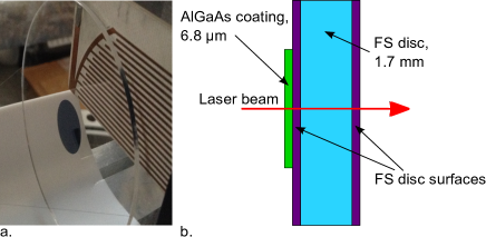
The crystalline AlGaAs coating stack is identical to that described by Cole et al [14] for which a direct thermal noise measurement was made. It consists of 40.5 bilayers of alternating GaAs and AlGaAs and is optimized for high reflectivity (HR) at a wavelength of 1064 nm. A circular stack 16.4 mm in diameter was bonded to a FS disc 3 ” in diameter and 1.7 mm in thickness (see Fig. 1 a.). We measured the optical absorption of the coating at a wavelength of 1530 nm, where the stack transmits 70 % of the laser power, using the PCI technique [16].
2.1 Absorption of the AlGaAs coating
PCI measures the change in phase of a portion of a large probe beam ( radius for the measurements presented here) caused by the absorption of light from a small pump beam (). The phase difference created by the pump beam within the probe beam is read out by measuring the interference between the light unaffected by the pump and the light which has been affected by the pump. This interference has a maximum value when measured approximately one (pump) Rayleigh range from the pump waist. The interferometric phase change measured at this point is directly proportional to the absorption of the material. The pump beam is amplitude modulated at a given frequency and a lock-in amplifier is used to recover the modulation of the interferogram at this frequency. The lock-in also provides the phase of this signal with reference to the pump modulation. This phase is determined by the diffusion of the heat from the pump absorption in the medium and by the pump beam dimensions. In the case where the transverse dimensions are much smaller than the change in intensity along the beam, the characteristic frequency is given by , where D is the thermal diffusivity of the material and is the beam waist. For modulation faster than this frequency the phase tends to , whereas for slower frequencies it tends to .
For the case of coating absorption, PCI and other methods which are based on heating assume an immediate heat transfer from the coating into the underlying substrate, and that the area of the substrate which is heated and therefore affects the probe beam is large compared to the thin coating [17, 18]. Amorphous coatings usually show a small thermal expansion coefficient and a small thermo-refractive coefficient d/d. So the phase change caused within a thin coating of only a few m, is small compared to the phase change caused within the substrate. These assumptions are valid for amorphous, sputtered coatings for which the majority of the signal is caused by the substrate while the signal produced directly in the coating is negligible.
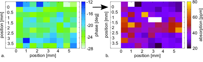
For the AlGaAs coating an area of 4 mm x 5.7 mm was mapped to check the homogeneity of the absorption. Figure 2 a. shows a map of the phase signal which provides two significant conclusions:
-
1.
The phase varies strongly for different positions on the coating.
-
2.
The mean value of differs significantly from the expected phase for the FS disc of for the used chopper frequency of 407 Hz.
The variation across the coating indicates a non-uniform heat conduction of coating and substrate (for an assumption of uniform coating and substrate material parameters) which may be related to variations in the quality of the bond between the coating and the substrate. The discrepancy of the mean phase from the expected phase for FS in general shows that the signal from the coating contributes significantly to the total signal.
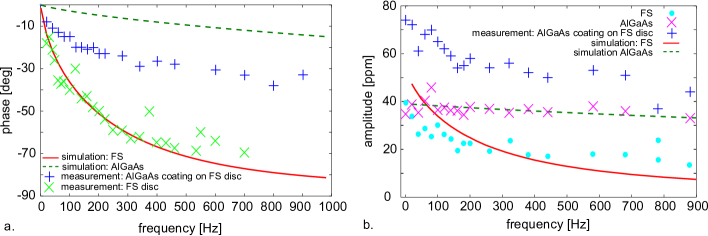
Figure 3 a. shows the development of the phase with chopper frequency for one position on the AlGaAs coating. The red solid line shows a simulation for FS. The measurement of the phase of an uncoated part of the FS disc is shown by the light green crosses () which is in agreement with the simulation. (The discrepancy for high frequencies is caused by low signal due to low/short heating). The green dashed line shows the theoretical frequency dependence of the phase for AlGaAs and the dark blue pluses (+) represent the phase measurement for the crystalline AlGaAs coating on the FS disc which is a mixture of and . Correspondingly the amplitude will also be a mixture of the amplitudes of FS and AlGaAs . The blue crosses () in Fig. 3 b. show a measurement of the amplitude for the AlGaAs on FS system. The total (amplitude and phase) signal for this AlGaAs coating on FS system is given by
| (1) |
From this we get the relations for the amplitudes
| (2) |
Using the phase information shown in Fig. 3 a. and Equs. 2 the measured amplitude for the mixed signal can be separated into the amplitude signals from the FS substrate and the AlGaAs coating . The light blue dots in Fig. 3 b. represent the part of the signal originating from the FS disc and the pink crosses () represent the part of the signal originating from the AlGaAs coating. The solid red and dashed dark green curves show corresponding simulations.
From a measured amplitude the absorption was calculated to be . The calibration factor was obtained by using a FS calibration sample with known absorption. For the FS fraction of the amplitude signal shown in Fig. 3 b., the calibration which was made with the FS sample is valid. For the AlGaAs component of the amplitude signal the absorption has to be recalibrated taking the material parameters into account which are given in Tab. 1. An additional calibration factor calculates from
| (3) |
to 1.04 at 407 Hz, where DFx is the dispersion function for surface absorption. For details see [16]. The measured absorption correspondingly calculates to
| (4) |
The calibration factor of 1.04 indicates that for the given material parameters and the measurement frequency, weighting of coating and substrate is very similar. This varies significantly for different materials and frequencies.
Figure 3 d. shows a map of the calibrated absorption after recalibration for each single measurement depending on the varying phase. The mean value of the absorption is (mean value and standard deviation). In subsection 2.4 this result is compared to the expected absorption for a highly reflective (HR) coating in which the vast majority of the light is reflected by only the first few layers of the coating.
| Parameter | FS Substrate | GaAs | AlGaAs |
|---|---|---|---|
| index of refraction (1530 nm) | [19] | [20] | [20] |
| index of refraction (1620 nm) | [19] | [20] | [20] |
| thermo refr. coeff. d/d [1/K] | [21] | [24] | [24] |
| specific heat [J/(kg K)] | [22] | [23] | [23] |
| density [] | [21] | [23] | [23] |
| thermal expansion [1/K] | [21] | [23] | [23] |
| thermal conductivity [W/(m K)] | [21, 22] | [23] | [23] |
2.2 Absorption of the (uncoated) fused silica disc
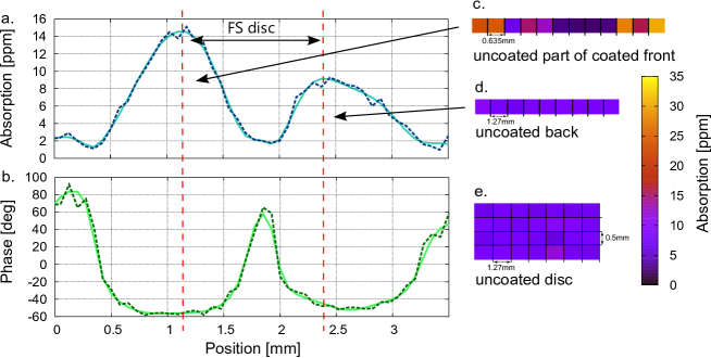
In a further step the absorption of an uncoated part of the coated face of the FS disc was measured. Figure 4a. shows the calibrated absorption signal of a scan through the FS disc, Fig. 4b. shows the corresponding phase signal. The red dotted lines mark the position of the substrate’s front (left) and back (right) surface. The absorption of the front surface is clearly higher than the absorption of the back surface. Therefore, we measured the absorption at several positions with 0.625 mm separation on the front surface (Fig. 4c.) and, after turning the disc around, repeated this measurement series for the back surface (Fig. 4d.). These measurements confirmed that the absorption of the back surface is (mean value and standard deviation) and therefore significantly smaller and more uniform than on the front surface with . For comparison we measured also the absorption of the surface of an identical, uncoated FS disc (Fig. 4e.). The absorption of this surface was and in good agreement with the absorption of the back side of the coated substrate.
The origin of the absorption increase and whether we can assume a similar surface absorption increase under the coating is unknown. The only difference in storing and treatment of the samples front and back surface was the plasma cleaning procedure used prior to the bonding process. The surface roughness of the front surface was found to be higher than the back surface by 25 % which would not necessarily increase the absorption but might increase the susceptibility to contamination.
Therefore, we can only give an upper limit for the absorption of the coating stack by subtracting the absorption of of the back surface resulting in . This corresponds to an absorption coefficient of and an extinction coefficient of at 1530 nm.
2.3 Intensity dependence of the absorption
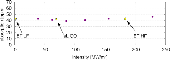
Semiconductor materials such as AlGaAs show two-photon absorption effects in which two photons are absorbed simultaneously to enable a carrier to cross the band gap. The band gap for AlGaAs is between 1.424 eV (871 nm, GaAs) and 2.16 eV (574 nm, AlAs). Therefore, we measured the intensity dependence of the absorption at one position of the coating. The intensity was varied between and . While the beam radius of was constant for all measurements the laser power was increased from 150 mW to 880 mW. This intensity range is above the intensity for ET LF () and includes the intensity for ET HF () and aLIGO (). The measurement series is presented in Fig. 5 and shows that the absorption of 42 ppm varies by less than within the studied intensity range. No significant increase at higher intensities was observed.
2.4 Comparison to HR coating
The AlGaAs coating stack is optimized for high reflectivity at 1064 nm while at 1530 nm we measured a transmission of approximately 70 %.
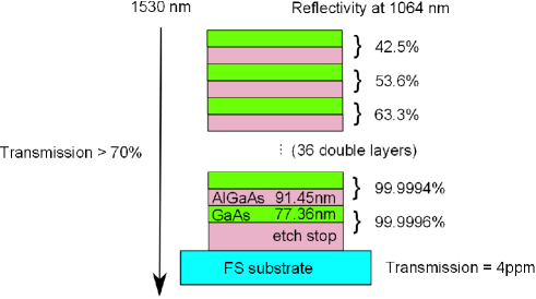
The coating is composed of alternating layers of GaAs and AlGaAs each with an optical thickness of a quarter of the wavelength of . With refractive indices of and at 1064 nm the optimal layer thickness would be 76.4 nm for GaAs and 89.3 nm for AlGaAs. The actual as-grown thicknesses of the layers are 77.36 nm for GaAs and 91.45 nm for AlGaAs.
At each layer boundary due to the change of refractive index light is reflected following Fresnel’s formulas [25]. To calculate the actual reflectivity and laser power within each double layer of the coating stack, the coating stack was simulated using ray-transfer matrix formalism for calculating a series of reflecting boundaries. Details can be found in [26].
The resulting reflectance of the coating stack per double layer shows that at 1064 nm 42.5 % of the input power is already reflected at the first double layer, 53.6 % at the second double layer etc. as indicated in Fig. 6. So the power within the first double layer is reduced to (100 - 42.5) %. The sum of the power per double layer results in an effective penetration depth of double layers of the input laser power into the coating stack. The total absorption measured would thus be equivalent to the absorption from 2.6 double layers which saw the full power of the laser. Repeating this calculation for a wavelength of 1530 nm results in double layers.
The ratio gives the scaling which is required to make the measured absorption comparable to the expected absorption for a stack designed to be highly reflective at 1530 nm with the additional consideration that the quarter wave single layers will be thicker by . Scaling the measurement using these factors results in which is in good agreement with previous results at 1064 nm and 1550 nm [27].
3 Summary and Conclusion
We have used photo-thermal common-path interferometry to measure the optical absorption at 1530 nm of an AlGaAs crystalline coating stack, designed for high reflectivity at 1064 nm and bonded to a FS disk.
The AlGaAs coating bonded to FS showed an unexpectedly large signal originating directly from the coating, requiring the simulation and analysis of the signal to be adapted.
To check the uniformity of the coating, an area of 4 mm 5.7 mm was mapped. The absorption of the complete stack as would be seen by the laser beam in a GW detector when transmitting the ITM was measured to be . This includes substrate surface absorption and a possible absorption of the bond in between substrate and coating. Subtracting the lower limit for the substrate surface absorption, forms an upper limit for the coating absorption. The corresponding absorption coefficient is (). This is equivalent to an absorption of in an AlGaAs stack designed for HR at 1530 nm. This is a very promising low absorption result for alternative low–loss coating materials. Still, further work will be necessary to reach the requirements of for future gravitational wave detectors.
Measurements of the phase show evidence of non-uniformity in the thermal contact between the coating and the substrate, which may indicate variations in the quality of the bond. These may be related to a insufficient quality of the substrate polish. The surface of the fused silica disk to which the coating was attached showed an increased absorption compared to the back surface of the sample. This is unexplained, but may be related to the plasma cleaning procedure used prior to bonding the coating.
One possible source of the measured AlGaAs absorption could be contaminants from the MBE growth process, which was carried out in a chamber used to deposit various materials including doped semiconductor layers. A dedicated AlGaAs MBE system, with reduced potential for contamination, may enable higher purity, and thus possibly lower absorption, coatings to be produced.
Acknowledgements
This work was partly funded by a Royal Society Research Grant (RG110331), and we are grateful for additional financial support from STFC and the University of Glasgow. IWM is supported by a Royal Society Research Fellowship. SR holds a Royal Society Wolfson Research Merit award. We are grateful to the International Max Planck Partnership for Measurement and Observation at the Quantum Limit for support, and we thank our colleagues in the LSC and VIRGO collaborations and within SUPA for their interest in this work. We thank Alexei Alexandrovski for valuable discussions.
This paper has LIGO Document number LIGO-P1400226.
References
References
- [1] Pitkin M, Reid S, Rowan S, Hough J 2011 Gravitational Wave Detection by Interferometry (Ground and Space) Living Rev. Relativity 14 5
- [2] Harry G M (the LIGO Scientific Collaboration) 2010 Advanced LIGO: the next generation of gravitational wave detectors Class. Quantum Grav. 27 084006
- [3] The Virgo Collaboration 2009 Advanced Virgo Baseline Design note VIR–027A–09 https://tds.ego-gw.it/itf/tds/file.php?callFile=VIR-0027A-09.pdf
- [4] Hild S 2010 A xylophone configuration for a third–generation gravitational wave detector Class. Quantum Grav. 27 015003
- [5] Adhikari R et al 2012 LIGO III Blue ConceptLIGO Technical Document LIGO-G1200573 dcc.ligo.org/LIGO-G1200573-v1/public
- [6] Harry G M et al. 2007 Titania–doped tantala/silica coatings for gravitational–wave detection Class. Quantum Grav. 24 405–415
- [7] Fine M E, van Duyne H and Kenney N T 1954 Low–Temperature Internal Friction and Elasticity Effects in Vitreous Silica J. Appl. Phys. 25 402–5
- [8] Rowan S, Byer R L, Fejer M M, Route R, Cagnoli G, Crooks D R M, Hough J, Sneddon P H, Winkler W 2003 Test mass materials for a new generation of gravitational wave detectors Proceedings of SPIE 4856 292–297
- [9] Winkler W, Danzmann K, Rüdiger A and Schilling R 1991 Heating by optical absorption and the performance of interferometric gravitational-wave detectors Physical Review A 44 7022–7036
- [10] McGuigan D F, Lam C C, Gram R Q, Hoffman A W, Douglass D H, Gutche H W 1978 Measurements of the mechanical Q of single-crystal silicon at low temperatures Journal of Low Temperature Physics 30 624–629
- [11] Nawrodt R et al. 2008 High mechanical Q-factor measurements on silicon bulk samples Journal of Physics: Conference Series 122 012008
- [12] Keevers M J, Green M A 1995 Absorption edge of silicon from solar cell spectral response measurements Appl. Phys. Lett. 66 174–176
- [13] Granata M et al. 2013 Cryogenic measurements of mechanical loss of high-reflectivity coating and estimation of thermal noise Optics Letters 38 24
- [14] Cole G D, Zhang W, Martin M J, Ye J and Aspelmeyer M 2013 Tenfold reduction of Brownian noise in high-reflectivity optical coatings Nature Photonics 7 644–650
- [15] Abernathy M et al. 2011 Einstein gravitational wave Telescope Conceptual Design Study www.ET-GW.eu
- [16] Alexandrovski A L, Fejer M M, Markosyan A, Route R 2009 Photothermal common-path interferometry (PCI): new developments Proc. SPIE 7193, Solid State Lasers XVIII: Technology and Devices 71930D doi: 10.1117/12.814813
- [17] Willamowski U 1998 Standardisierbare Verfahren zur präzisen Charakterisierung des Absorptions-, Reflexions- und Transmissionsgrads optischer Komponenten PhD Thesis LU Hannover, Germany
- [18] Steinlechner J, Jensen L, Krüger C, Lastzka N, Steinlechner S, and Schnabel R 2012 Photothermal self-phase-modulation technique for absorption measurements on high-reflective coatings Appl. Opt. 51 1156–1161
- [19] Leviton D B, Frey B J 2006 Temperature–dependent absolute refractive index measurements of synthetic fused silica Proc. SPIE 6273 Optomechanical Technologies for Astronomy 62732K
- [20] Afromowitz M A 1974 Refractive Index of Ga1-xAlxAs Solid State Communications 15 59–63
- [21] Weber M J 2003 Handbook of Optical Materials CRC Press ISBN 0-8493-3512-4
- [22] http://accuratus.com/fused.html
- [23] www.ioffe.ru
- [24] Kim J P, Sarangan A M 2007 Temperature–dependent Sellmeier equation for the refractive index of AlxGa1-xAs Optics Letters 32 5
- [25] Hecht E 2012 Optics Pearson Education, ISBN 8131718077
- [26] Steinlechner S 2013 Quantum metrology with squeezed and entangled light for the detection of gravitational waves PhD Thesis LU Hannover, Germany
- [27] http://www.crystallinemirrors.com