Engineering polar discontinuities in honeycomb lattices
Abstract
Unprecedented and fascinating phenomena have been recently observed at oxide interfaces between centrosymmetric cubic materials, such as LaAlO3 and SrTiO3, where a polar discontinuity across the boundary gives rise to polarization charges and electric fields that drive a metal-insulator transition, with the appearance of free carriers at the interface. Two-dimensional analogues of these systems are possible, and honeycomb lattices could offer a fertile playground, thanks to their versatility and the extensive on-going experimental efforts in graphene and related materials. Here we suggest different realistic pathways to engineer polar discontinuities across interfaces between honeycomb lattices, and support these suggestions with extensive first-principles calculations. Two broad approaches are discussed, that are based on (i) nanoribbons, where a polar discontinuity against the vacuum emerges, and (ii) selective functionalizations, where covalent ligands are used to engineer polar discontinuities by selective or total functionalization of the parent system. All the cases considered have the potential to deliver innovative applications in ultra-thin and flexible solar-energy devices and in micro- and nano-electronics.
Combining together different materials rarely results in a simple “arithmetic sum” of their properties. Typically, the composite system displays properties that are not present in its components, giving rise to novel and unexpected behavior. This is the case for oxide interfaces, which have been recently attracting considerable attention, both experimentally and theoreticallyMann2010 ; Hwa2012 . Among these, a dominant role is played by heterostructures of strontium titanate (SrTiO3 or STO) and lanthanum aluminate (LaAlO3 or LAO). Both LAO and STO are insulators; nevertheless, when brought together, a two-dimensional electron gas (2DEG) with high mobility appears at their interfaceOht2004 . This 2DEG is host to a rich variety of phenomena, ranging from superconductivityRey2007 to magnetismBri2007 (and even the unprecedented combination of the twoLi2011 ; Bert2011 ), with many promising device applications. The most intuitive picture to explain the existence of the 2DEG follows from dielectric considerations on the bulk properties of the constituent compoundsBris2014 . LAO and STO have an identical cubic centrosymmetric crystal structure; therefore, classically, the macroscopic polarization of each material should be zero, thanks to inversion symmetry. However, in the framework of the Modern Theory of PolarizationResta1994 , polarization cannot be represented by a single vector, but as a lattice of vectors with the same periodicity of the crystal lattice and satisfying all the symmetries of the crystal. For cubic systems that display inversion symmetry, this condition allows two different polarization lattices, one containing the zero vector, and another shifted by half of the cube diagonal. STO belongs to the first class, while LAO to the second and, as a result, a polar discontinuity appears when LAO is epitaxially grown on top of STO and a polarization charge builds up at the interfaceBris2014 . This discontinuity creates an electric field inside LAO that can in turn induce a metal–insulator transition with a transfer of free charges from the surface of LAO to the STO/LAO interfaceBris2014 ; Jano2012 . This transition has been found experimentally to occur at LAO thicknesses of 3-4 layersThi2006 , in agreement with theoretical calculationsBris2014 .
Such concepts could be extended to lower dimensions, with one-dimensional (1D) channels of free carriers appearing at the boundary between two-dimensional (2D) insulating materials, provided that the “bulk” polarizations of the 2D crystals involved were different. In this respect non-centrosymmetric honeycomb lattices offer a very promising playground, owing to the quantized and topological nature of their bulk polarizationFang2012 ; Jad2013 . A suggestion in this direction has been put forward in Ref. Bris2013, , where the authors have considered honeycomb crystals of aluminum nitride (AlN), silicon carbide (SiC), and zinc oxide (ZnO). First-principles simulations have confirmed the existence of a polar discontinuity at the interface between two such crystals, with free charges accumulating in 1D channels along the interfacesBris2013 . In the thermodynamic limit, the linear charge density of free carriers perfectly balances the polarization charge density and it is thus determined solely by the bulk properties of the materials involved and by the orientation of the interface throughVand1993
| (1) |
Here are the bulk polarizations of the parent crystals and is a unit vector normal to the interface and pointing from 1 to 2. Although the suggestion for an analogue in 2D of the LAO/STO heterostructure is very promising, a practical concern hinders the feasibility of the setup suggested in Ref. Bris2013, . Indeed, although ZnO and SiC have been synthesized as few-layer hexagonal structuresTus2007 ; Lin2012 , they have not been isolated as monolayers, and the realization of in-plane heterostructures seems even more demanding.

In this paper we outline instead experimentally viable approaches to the realization of polar discontinuities at the interface between honeycomb structures, giving rise to 1D wires of electrons and holes and opening the possibility of manifold applications.
First, we note that vacuum can be interpreted as an insulator with vanishing polarization. Thus, in a nanoribbon made out of any polar lattice, polarization charges will appear as a consequence of the polar discontinuity at its edges (i.e., at the interface with vacuum). Second, we argue that covalent functionalizations (for instance with hydrogen or fluorine) can change the polarization of the parent crystal. Partial functionalization of a 2D sheet thus introduces a discontinuity in the electric polarization at the boundary between functionalized and pristine regions. Alternatively, full functionalization of the recently reportedSut2012 ; Lev2012 ; Liu2013 ; Liu2014 ; Gong2014 lateral heterostructures between graphene and boron nitride can also be pursued. We illustrate in the following all these strategies in more detail, starting from those that are conceptually simpler and highlighting for each the challenge or simplicity of their experimental realization. Last, we support these suggestions with the results of extensive first-principles numerical simulations.
Nanoribbons: sp materials
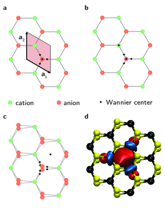
As a first suggestion we consider the case of pristine nanoribbons (see Fig. 1a) where the discontinuity has to be considered with vacuum. According to the interface theoremVand1993 , the polarization charge density is related to the bulk formal polarizationResta1994 which, for non-centrosymmetric honeycomb crystals, is constrained by symmetry to have quantized values and to point along one of the equivalent armchair directionsFang2012 ; Jad2013 ; Bris2013 :
| (2) |
In equation (2) and are the primitive lattice vectors (see Fig. 2), is a generic Bravais lattice vector, is the area of a unit cell, and . The value of can be simply obtained once the ground state of the system is expressed in terms of a set of maximally-localized Wannier functionsMar2012 . In addition, the apparent ambiguity in the choice of the lattice vector in equation (2) can be lifted by properly assigning each Wannier function to a given ion according to the crystal terminationSte2011 . Then, the electronic contribution to can be expressed as a sum over point-like charges located at the Wannier centers and the total formal polarization reads
| (3) |
Here and are the charges and positions of the ions in the unit cell and is the number of electrons. Let us first consider heteroatomic honeycomb lattices in which the electronic properties are determined by s and p orbitals, such as BN (monolayer SiC and ZnO, if realized, would also belong to this class). In Fig. 2a we show the Wannier function centers of such systems and by using equation (3) it is easy to show that the bulk formal polarization can be non-zero (see also Supplementary Information). A finite polarization charge thus appears at the edges of a nanoribbon made out of one of these honeycomb crystals, provided that the edge is not parallel to Vand1993 . We have verified that indeed the polarization charge vanishes for armchair nanoribbons while it is maximal for perfect zigzag nanoribbons.
Looking at, e.g., the ideal case of zigzag edges, the polarization-induced electric field shifts the energy bands of the ribbon linearly in space, reducing the effective gap of the system. By increasing the width of the nanoribbon, a metal-insulator transition occurs as the top of the valence band reaches in energy the bottom of the conduction band. As shown in Fig. 1a, free carriers localize close to the edges of the nanoribbon with different character (electron or hole) on opposite sides. The density of free carriers at each edge increases with the width of the nanoribbon and, asymptotically, perfectly screens the polarization charge in agreement with equation (1). It is thus possible to tune such nanoribbons from a regime of small widths (few nanometers) in which there is a sizable electric field and negligible density of free carriers to an opposite regime for large widths (tens of nanometers or more) of vanishing electric fields but high metallicity.
Metallicity of heteroatomic zigzag nanoribbons has been investigated theoretically in recent yearsBar2008 ; Bot2008 ; Lou2011 , and it has been pointed out that such 1D metallic channels can undergo magnetic transitions and eventually become half-metallic. However, no connection with the intrinsic polarization of the parent materials and with the existence of finite electric fieldsQi2012 has been drawn yet. As we shall discuss later, this is actually one of the key features that make some of these systems very promising for solar-energy applications.
It is important to mention that, depending on the edge termination, additional charges might appear at the boundaries. For instance, by terminating edge bonds with hydrogen, an additional charge per unit length is introduced at opposite edges. Therefore, any specific termination does not neutralize the total charge at the edge, since termination effects can change it only by an integer number of electrons per unit length, while the polarization charge is typically a non-integer fraction of an electron per unit length. The only relevant exception are pristine III-V ribbons (i.e. exactly BN) for which , so that termination-induced charges might completely screen polarization effects. On the other hand, functionalized BN ribbons, discussed later, would be resilient against such mechanism. In addition, even in the case with , by applying strain it would be possible to tune the polarization charge while leaving unaffected the termination effects, thus restoring a finite electric field (see also the Supplementary Information for a detailed description of termination effects).
From an experimental point of view, the main challenge would be to control the edge structure and chemistry. On the other hand, recent progressTreier2011 ; Kim2013 ; Zha2013 in atomistic control over the edge structure of graphene nanoribbons has been quite spectacular and could be foreseeably extended to other honeycomb crystals.
Nanoribbons: transition metal dichalcogenides
In addition to sp materials, other honeycomb lattices can support a finite bulk polarization, starting from transition metal dichalcogenides (MX2). Although these materials have been extensively studied in the last few yearsWang2012 ; Chh2013 , their bulk formal polarization has not been discussed so far. In such systems one sublattice is occupied by a transition metal M while the other hosts two chalcogens X displaced in the vertical direction on opposite sides with respect to the plane of M atoms. In Fig. 2c we show the Wannier function centers for the top seven valence bands when the transition metal belongs to group VI (M=Mo, W). Six centers lie close to the S atoms, which play the role of “anions” (see also Supplementary Information), while the last one is located at the center of the hexagonal cell and is associated with the Wannier function displayed in Fig. 2d. As a consequence, group-VI transition metal dichalcogenides like MoS2 have a non-trivial (i.e. ) formal polarization and their nanoribbons support a polar discontinuity, in exact analogy with what happens for sp materials. In addition, we mention that a polar discontinuity occurs also across inversion domain boundariesZhou2013 ; Zan2013 ; Liu2014b that lie along zigzag directions and separate crystallites with opposite polarizations. Thus, transition metal dichalcogenides offer a broad choice in materials, chemistry, and electronic structure, and represent one of the most promising experimental avenues to pursue. Indeed, polarization effects might be at the origin of metallic states already observed at inversion domain boundaries in MoSe2Liu2014b and at the edge of MoS2 nanoclustersHel2010 .
Selective functionalization
As a second different route to engineer polar discontinuities we suggest covalent atomic functionalizations, such as those with hydrogen or fluorine. We assume full coverage and we consider for simplicity a chair conformation, corresponding to functionalizations in alternating positions above and below the plane of the parent honeycomb lattice (see Supplementary Information for a discussion on the different conformations of functionalized BN and their thermodynamic stability). In Fig. 2b we show the Wannier function centers for a typical functionalized honeycomb lattice. We report results only for the case of hydrogen, since the case of fluorine is completely analogous. It is easy to verify that these covalent functionalizations change the value of in equation (2) by one unit with respect to the parent material. As a consequence, we first note that functionalized nanoribbons would still support a polar discontinuity at the edges (and in particular III-V materials become less sensitive to termination-induced charges as changes from 0 to 1, see Supplementary Table S1). Second, selective functionalization of a parent honeycomb lattice would create an interface between pristine and functionalized regions, introducing a polar discontinuity in the system. This situation is depicted in Fig. 1b, where we consider perfect zigzag interfaces (giving rise to the largest polar discontinuity) between alternating stripes of pure and hydrogenated BN, similarly to what happens in graphene “nanoroads”Singh2009 . As expected, free carriers localize at opposite interfaces.
This case will be discussed at length in the last part of the paper, but we point out that the two regions (pristine and functionalized) remain obviously aligned with respect to each other and are close to a perfect lattice match (e.g., for BN: Å and Å). The experimental challenge is thus shifted to the selective functionalization of the parent crystal. In order to achieve this result, it is likely that techniques adopted for the functionalization of grapheneKar2013 ; Joh2013 could be generalized to heteroatomic honeycomb crystals. Indeed, full coverage, double-sided hydrogenation of graphene (i.e. graphane) has been realized in suspended samples by exposure to low-temperature hydrogen plasmasEli2009 . As far as fluorographene is concerned, a 1:1 carbon to fluorine ratio is achievable by functionalization with atomic fluorine formed by decomposition of xenon difluoride (XeF2)Nair2010 ; Rob2010 . By combining this technique with scanning probe lithography a pristine graphene nanoribbon has been isolated within a matrix of partially fluorinated grapheneLee2011 . In addition, encouraging results have been already reported on the partial fluorination of BN nanotubesTang2005 and nanosheetsXue2013 .
| Methods | Materials | |
|---|---|---|
| Nanoribbons | BN, functionalized BN, | |
| transition metal dichalcogenides (MoS2, …) | ||
| Inversion domain boundaries | transition metal dichalcogenides | |
| Selective functionalization | BN | |
| Full functionalization | graphene/BN heterostructures |
Functionalized graphene/boron nitride interfaces
In view of the well-established experimental technology in growing single layer graphene and boron nitride and the recent achievementsSut2012 ; Lev2012 ; Liu2013 ; Liu2014 ; Gong2014 in obtaining sharp graphene/BN lateral heterostructures, it is of great interest to exploit these materials to engineer a polar discontinuity. While pristine graphene is not an insulator and does not support a bulk polarization, its functionalized forms (graphaneEli2009 and fluoro-grapheneNair2010 ; Rob2010 ) are insulators and their formal polarization is constrained by symmetry to be zeroFang2012 ; Jad2013 . Moreover, we have seen above that functionalized BN acquires a non-trivial bulk polarization (). Thus, full functionalization of existing planar graphene/BN heterostructuresSut2012 ; Lev2012 ; Liu2013 ; Liu2014 ; Gong2014 will lead to the emergence of a polar discontinuity and a finite density of free carriers at the interfaces, as shown in Fig. 1c (we stress that this mechanism is completely different from the one that leads to metallicity in unfunctionalized graphene/BN interfacesPru2010 ). In addition, the intrinsic preference of these interfaces to grow along a zigzag directionSut2012 ; Liu2014 provides the optimal orientation to maximize the polar discontinuitiy.
Functionalized nanotubes
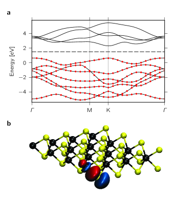
Although this paper is mainly devoted to 2D systems, we would like to illustrate what happens when these honeycomb lattices are rolled up in nanotubes and a finite polarization along the axis arises depending on the chirality of the nanotubeNak2003 . Focusing on zigzag nanotubes, by selective functionalization one can introduce a polar discontinuity along the tube, as illustrated in Fig. 1d. Similarly to what happens in 2D, a finite polarization charge builds up at the interfaces, creating an electric field that induces a charge reconstruction, with the appearance of electron- and hole-rich quantum dots. The charge density localized in these quantum dots is shown in Fig. 1d in the case of a (8,0) BN nanotube with selective hydrogen functionalization. The reduced dimensionality suggests that the effects of Coulomb interactions might be relevant for the electronic-structure properties of such quantum dots, similarly to what happens in carbon-nanotube quantum dotsSap2006 . The interaction-driven phenomena that might arise would then be interesting both from a fundamental and practical point of view, with particular emphasis towards quantum information applicationsLos1998 . In addition, even in the regime of small system sizes (when no charge is transferred in the quantum dots), the magnitude of the electric field in each segment might be easily tuned by varying the diameter of the nanotube and the distance between the interfaces. As we shall discuss in the following, this has significant consequences in solar-energy applications.
Results and discussion
In order to support the general arguments presented above, we now use detailed, large-scale first-principles simulations to investigate a paradigmatic case study. For definiteness we focus on selective hydrogen functionalization of BN (that we label as BNH2), even though qualitatively similar results can be obtained using different parent materials and functional atoms or any of the alternative approaches discussed above (and summarized in table 1).
We simulate interfaces between pristine and functionalized BN within periodic boundary conditions, considering superlattices obtained by alternating BN and BNH2 regions. As a consequence, two opposite interfaces are present within a simulation supercell, which is identified by two primitive lattice vectors. The first one defines the periodicity along the interface and can be determined by specifying the number of zigzag and armchair sections present, as shown in Fig. 3b: ( and are positive coprime integers while and are translation vectors along the zigzag and armchair direction, respectively). The second lattice vector defines the periodicity of the superlattice in terms of the number of unit-cell repetitions that define the width of each region. It is important to mention that the lattice vector alone is not sufficient to uniquely define the interface, since one still needs to specify the shape of the boundary (i.e. which lattice sites should be assigned to each side of the interface). For simplicity we consider only interfaces that minimize the number of boundary atoms and bondsAkhm2008 . Different choices would affect only quantitatively the results, through the appearance of additional bound charges at the interface.
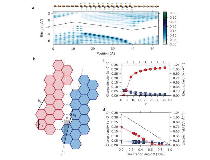
We first focus on the case of a perfect zigzag interface (), when we have a finite polarization charge density with opposite signs at each interface. These polarization charges create an electric field inside both BN and BNH2, as can be clearly seen in Fig. 3a examining the finite slope of the macroscopic and planar averageBal1988 of the electrostatic potential energy (solid line). In Fig. 3 we also show the average local density of states (LDOS) as a function of energy and position along the direction orthogonal to the interfaces. As a consequence of the electric fields, the electronic bands shift linearly as a function of position. For sufficiently large widths (as in Fig. 3a), this leads to an energy overlap between the conduction and valence bands of the two interfaces, and to a charge redistribution with the creation of electron and hole pocketsJano2012 ; Bris2013 . The Fermi energy (dashed line) intersects both the top of the valence band and the bottom of the conduction band so that the system has become metallic, as expected. Fig. 1b shows the excess charge density obtained by integrating the LDOS in order to take into account the partial depletion of the valence bands (for holes) and the filling of the conduction bands (for electrons). Both figures make it clear that excess electrons and holes are separated in space and reside on opposite interfaces, partially screening the polarization charges. In Fig. 3c we report the density of free carriers for different widths of the ribbons (red circles). As the periodicity of the superlattice increases, the charge of free electrons and holes also increases as a result of a larger overlap between conduction and valence bands. Since the free charge has an opposite sign with respect to the polarization charge, the overall charge density at each interface decreases together with the electric field in both materials (blue triangles in Fig. 3c). Asymptotically, the free charge completely balances the polarization charge according to equation (1) and the electric fields vanish, thus preventing a polar catastropheBris2014 . Indeed, in Fig. 3c the density of free carriers approaches asymptotically the polarization charge obtained from the bulk formal polarizations of BN and BNH2 (black solid line). If the two materials were perfectly lattice-matched we would have, from the discussion on Wannier functions above [equations (1) and (2)], that . Owing to the piezoelectric properties of these materials, is slightly larger than as a result of the finite strain necessary to reach a common equilibrium lattice constant along the interfaceBris2013 .
Let us now consider an arbitrary interface orientation that can be identified by the angle between the lattice vector along the interface, , and the pure zigzag direction, , so that
| (4) |
According to equations (1) and (2) the polarization charge density gradually decreases down to zero as goes from zero (pure zigzag, ) to (pure armchair, ). In particular, neglecting for simplicity piezoelectric effects, we find
| (5) |
Thus, we expect that the appearance of finite electric fields and the presence of a metal-insulator transition are not restricted to the case , although their effects are depressed as we approach . Fig. 3d shows the free charge density and the electric fields in BN and BNH2 for several values of corresponding to different combinations of and . All simulations have been performed keeping fixed the periodicity of the superlattice (). Despite the small width of the system, the free charge density survives over a wide range of angles, thus suggesting robustness with respect to the interface orientation. In addition, by incrementing the periodicity of the superlattice the free charge density could be further increased and asymptotically reach the solid line representing the polarization charge in equation (5), as it happens in the case shown in Fig. 3c.
Conclusions
We have presented different approaches to obtain polar discontinuities in honeycomb lattices, supporting these predictions with first-principles simulations. First, we highlight that a finite-width nanoribbon introduces a polar discontinuity with vacuum if the parent material supports a finite formal polarization. This happens for heteroatomic honeycomb crystals such as boron nitride and its functionalized derivatives, and for transition metal dichalcogenides, such as molybdenum disulfide. The existence of a polar discontinuity at the edges elucidates why metallicity can arise in honeycomb nanoribbonsBar2008 ; Bot2008 ; Lou2011 or at inversion domain boundariesLiu2014b . Second, we show that covalent atomic functionalizations, e.g. with hydrogen or fluorine, can change the bulk polarization of a honeycomb lattice. Thus, covalent functionalizations can be used to engineer polar discontinuities in 2D materials or 1D nanotubes simply by introducing interfaces between functionalized and pristine sections. In addition, since covalent functionalizations open a gap in graphene, they can be exploited to engineer polar discontinuities in existing graphene/BN interfacesSut2012 ; Lev2012 ; Liu2013 ; Liu2014 ; Gong2014 , without the need for selective functionalization.
We believe that engineering polar discontinuities in honeycomb lattices will provide a novel platform for manifold applications. First, 1D channels of free carriers along the interfaces could be exploited for circuitry in new-generation ultra-thin and flexible electronics. Indeed, current signals between different units of a device could be transmitted along such 1D channels, surrounded by insulating bulk materials, exceeding the limits of lithography in current electronic devices. Moreover, the reduced dimensionality of the channels gives rise to magnetic instabilitiesBris2013 that could be useful in spintronics applications. Second, and even more compelling, we envision a fruitful employment in solar-energy technology for the realization of light-harvesting devices. Indeed, the “bulk” interior of these systems is insulating and is an active region where photons can be absorbed, creating electron-hole pairs. For narrow systems, the polarization charges at the interfaces or edges are not compensated and thus naturally create an electric field (we note in passing that this is different from what has been done in recent photovoltaic devices based on transition metal dichalcogenidesPosp2014 ; Bau2014 ; Ross2014 ; Jo2014 , where metallic gates have been employed to create a - junction). Once the electron-hole pair is created, the electric field separates the electron and the hole and guides them towards opposite interfaces, where the 1D wires naturally collect and transport them. In addition, the electric field shifts in space the conduction and valence band extrema, and creates a variable effective gap depending on the spatial extension of the exciton, with an ensuing tunability of the cell efficiency. Furthermore, several systems with different widths and materials composition could be integrated into a single device in order to optimize the range of photon frequencies that can be absorbed.
Methods
All first-principles calculations reported here are carried out within density-functional theory (DFT) by using the PWscf code of the Quantum-ESPRESSO distributionGian2009 with the Perdew-Burke-Ernzerhof exchange-correlation functionalPBE . An ultrasoft pseudopotential descriptionVand1990 of the ion-electron interactions is adopted. Energy cutoffs are set to 60 Ry and 300 Ry respectively for the electronic wavefunctions and the charge density in the case of BN/BNH2 superlattices. For zigzag interfaces a shifted Monkhorst-Pack grid is used to sample the Brillouin zone together with a Ry Marzari-Vanderbilt smearingMarz1999 . In order to simulate a 2D system irrespective of the three-dimensional periodicity requirements of plane-wave basis sets, a vacuum layer of 20 Å is added between periodic replicas in the vertical direction. Relaxed structures are obtained within the Broyden-Fletcher-Goldfarb-Shanno method by requiring that the forces acting on atoms are below 0.026 eV/Å and the residual stress on the cell is less than 0.5 kbar. Some simulations have been performed without relaxation in order to simplify the calculations without qualitatively affecting our results. We notice that the well-known DFT limitations in predicting energy gaps influence only quantitatively the relation between free charge density, electric fields, and width of the system, without changing the general physical picture or its asymptotic limits. Maximally-localized Wannier functions have been computed using Wannier90Wannier90 . We created figures of structures and charge densities using VMDVMD .
Acknowledgements
Simulation time was provided by the Swiss National Supercomputing Centre (CSCS) through project ID s337; M.G. acknowledges partial support by the Max Planck–EPFL Center for Molecular Nanoscience and Technology. This research was stimulated by a talk of E. Artacho on the work of Ref. Bris2013, .
Author contributions
M.G., G.P. and N.M. conceived the work; M.G. and G.P. performed the first-principles simulations, and M.G., G.P. and N.M. wrote the manuscript.
Competing financial interests
The authors declare no competing financial interests.
Supplementary Information
Effects of termination in nanoribbons
Whenever a honeycomb crystal supports a finite formal polarization, a polar discontinuity arises at the interface with vacuum, as for instance in finite-width nanoribbons. We thus expect a finite electric field to be present as a result of the polarization charge density that appears at the edges. This electric field will in turn trigger a metal–insulator transition with increasing width of the nanoribbon. On the other hand, depending on the specific termination of the nanoribbon, we may have additional bound charges at the edges that partially screen the polarization charge. These contribute to the total bound charge density at each edge with a integer multiple of per unit length. According to equation (2), the total bound charge density at the edge for a zigzag nanoribbon reads
| (S1) |
As we mentioned in the paper, the integer is completely determined by the bulk properties of the system, while the integer depends on the specific termination of the nanoribbon. We thus have that whenever , the total charge at the edge (and consequently also the corresponding electric field) might vanish depending on the nanoribbon termination. To show this, in Fig. S1a we plot the macroscopic average (black lines) on top of the planar average (gray lines) of the electrostatic potential energy across a BN nanoribbon (, see table SI), including also a region of vacuum on both sides of the ribbon. We see that an electric field is present when edge bonds are unpassivated (solid lines, , i.e. ) while it disappears when bonds are saturated with hydrogen (dashed lines, , i.e. ). A finite electric field is restored (although with opposite sign) when dangling bonds of edge atoms are saturated with two hydrogen atoms (dotted lines, , i.e. ).
On the contrary, when a non-vanishing bound charge (and the corresponding electric field) will always be present at the edges irrespective of the termination, although it may change sign depending on the value of . Indeed, the polarization charge in these cases is fractional and thus can not be completely screened by an integral termination-induced edge charge. This is shown in Fig. S1b in the case of ZnO (, see table SI). The electric field associated with the polarization charges is always different from zero, although it changes sign as the polarization charge goes from (i.e. , ) for unpassivated edge bonds (solid lines) to (i.e. , ) for hydrogen-terminated bonds (dashed lines). We mention that similar conclusions apply also for functionalized BN nanoribbons (, see table SI).
| Material class | Nanoribbon | Selective functionalization | |
|---|---|---|---|
| BN | 0 | ✗11footnotemark: 1 | ✓ |
| BNH2 | 1 | ✓ | |
| MoS2 | 1 | ✓ | ✓22footnotemark: 2 |
| SiC | 2 | ✓ | ✓ |
| SiCH2 | 0 | ✗11footnotemark: 1 | |
| ZnO | 1 | ✓ | ✓ |
| ZnOH2 | 2 | ✓ |
1 In this case a polar discontinuity is still possible but some nanoribbon edge terminations can remove it.
2 In principle selective functionalization works for transition metal dichalcogenides, even though it would be difficult to realize in practice.
To summarize, in nanoribbons made of materials for which in equation (2) the polarization charge can not be completely screened irrespective of the edge termination and thus a finite electric field is always present, which induces a metallic state for sufficiently large widths. Nanoribbons with might still support a finite electric field but would be more susceptible to termination-induced effects. Finally, we stress that while the termination-induced bound charge can be obtained by charge counting and does not depend on strain, the polarization charge is affected by strain through the piezoelectric response of the system. This means that even when in equation (S1), we can still apply strain to restore an unbalanced polarization charge and thus a finite electric field.

Wannier functions of transition metal dichalcogenides
In order to compute the bulk formal polarization of transition metal dichalcogenides like MoS2 we need the centers of the Wannier functions associated with the valence bands. Including the deepest electronic states into the ionic cores, we are left with six electrons in the outermost d-orbitals of the transition metal and four p-electrons for each chalcogenLeb2009 . These atomic orbitals give rise to the eleven bands shown in Fig. S2a. Seven of them are fully occupied (valence bands) and separated from the lowest four conduction bands by a direct energy gap at the Brillouin zone corners. Here and in the following we focus on the representative case of MoS2 although similar conclusions can be drawn for other isoelectronic compounds like MoSe2 or WS2. A standard localization procedure Mar2012 allows us to associate the six lowest valence bands with as many Wannier functions that are localized on sulphur atoms with lobes pointing towards one of the nearest neighbors (see also Fig. 2c in the paper). As shown in Fig. S2b, such Wannier functions arise from the hybridization between p-orbitals on sulphur and d-orbitals on molybdenum. Less trivial is the topmost valence band, which is disentangled from the others. A careful analysis shows that this isolated band can be mapped into a rather broad Wannier function with a dominant d-character, located at the center of the hexagonal unit cell (see Fig. 2d in the main paper). As a measure of the reliability of these Wannier functions we show in Fig. S2 that a Wannier interpolation procedure Mar2012 is able to reproduce precisely the first-principles valence band structure. In addition, by applying equation (3), it is possible to prove that for MoS2 (and similarly for all other group-VI transition metal dichalcogenides).
Conformers of functionalized honeycomb lattices

| (eV/atom) | (eV/atom) | (eV/atom) | ||
|---|---|---|---|---|
| H | chair | |||
| boat | ||||
| stirrup | ||||
| F | chair | |||
| boat | ||||
| stirrup |
As we mentioned in the paper, selective functionalization of a parent heteroatomic honeycomb crystal (like BN) introduces a polar discontinuity in the system. We focused in particular on covalent hydrogenation or fluorination, when H or F atoms are adsorbed on both sides of the honeycomb lattice similarly to what happens in graphane and fluorographene. Several configurations are possible, depending on the pattern formed by the adsorbed atoms above and below the 2D sheet. Taking boron nitride as parent honeycomb lattice, Fig. S3 shows the configurations compatible with an eight-atom unit cell: (a) chair, (b) boat, and (c) stirrupSof2009 ; Bha2011 . By projecting the atomic positions in plane, we notice that their 2D spatial group (wallpaper group) is different, being cm for boat and stirrup isomers while p3m1 for the chair structure. According to Ref. Jad2013, the chair configuration is the only one compatible with a quantized (topological) polarization [see equation (2)]. For the other conformers, instead, symmetry only constrains one component of the in-plane polarization vector, leaving the other one completely undetermined. Even though in principle the chair configuration could seem to be optimal since it ensures a stable (topological) polarization, the strain arising from the lattice mismatch between pristine and functionalized forms breaks the symmetries that protect quantization. In addition, we shall see that all conformers support a different polarization with respect to the parent material and thus give rise to a polar discontinuity. For these reasons, all conformers give rise to analogous physical effects, and only the chair configuration has been discussed in the paper for the sake of simplicity since it shares the same (2D) symmetry of the parent material and thus its bulk polarization can be expressed through equation (2).
For the purpose of engineering a polar discontinuity, all configurations are in principle equally relevant and one needs to assess their relative stability. In table SII we focus on boron nitride and we report the ground-state energy together with atomic and molecular formation energies (per atom) of the three configurations for both hydrogenated and fluorinated structures. The atomic formation energy is defined as
| (S2) |
while the molecular formation energy reads
| (S3) |
In equations (S2) and (S3), is the total energy of functionalized BN in its optimized geometry, the total energy of the parent BN sheet, the number of H or F atoms, and () their atomic (molecular) total energy. A negative atomic (molecular) formation energy reveals if the functionalization is likely a favorable process in the presence of the adsorbate in atomic (molecular) form. We immediately notice that for hydrogenated BN the chair configuration not only has a positive molecular formation energy, but it is even less stable than the boat and stirrup isomers. This is in agreement with previous results on a similar level of theory Aver2009 ; Wang2010 ; Bhat2010 ; Sam2012 . On the contrary, for fluorinated BN the repulsion between fluorine atoms favors a situation in which neighboring F atoms are on opposite sides of the BN sheet. As a consequence, the chair configuration is the most stable, with both the atomic and molecular formation energies being negative. Since functionalization is typically performed in atomic atmosphere, our results suggest that both fluorination and hydrogenation are achievable for BN. Although these results based on equations (S2) and (S3) are valid only in the limit of zero temperature, we have verified that our conclusions do not change even at standard ambient temperature and pressure conditions. Indeed, by replacing in equations (S2-S3) the total atomic or molecular energy with the chemical potential of the gas (including translational, rotational, vibrational, and nuclear contributions), the gain in formation (free) energy reported in table SII decreases by less than 0.3 eV/atom.
We now want to verify that a polar discontinuity between pristine and functionalized honeycomb lattices arises irrespectively of the specific configuration (chair, boat, or stirrup) of the adsorbed atoms. In order to compute the bulk formal polarization, we need the Wannier function centers for each conformer. These are shown in Fig. S3 in the case of hydrogenated BN. We report results only for hydrogen since the case of fluorine is completely analogous. In fact, the six additional positive ionic charges of F with respect to H are completely balanced by three additional Wannier functions that are symmetrically arranged around the F atom. We notice that the three configurations are qualitatively very similar: In each unit cell we find a Wannier function centered approximately mid-bond between each H and N or B atoms and other three around each anion (N in this case) along directions pointing towards its nearest B neighbors. For the chair conformer, this is in agreement with the schematic picture in Fig. 2b. Thus, only minor quantitative variations occur between the conformers, while more radical qualitative features distinguish them from pristine BN as already mentioned in the paper (see Figs. 2a and b). In particular the formal polarization is always orthogonal to the zigzag direction and reads (in units of ): (chair), (boat), (stirrup), and (pristine BN). Although piezoelectric contributions should be taken into account when considering interfaces, this analysis already shows that for any conformer selective hydrogenation leads to a polar discontinuity in BN honeycomb lattices. Indeed, we have verified (through a more careful simulation of a zigzag interface between pristine and functionalized BN) that free charges appear at the boundaries as a result of the polarization-induced electric fields independently of the specific arrangement (chair, boat, or stirrup) of hydrogen atoms.
References
- (1) J. Mannhart and D. G. Schlom, Science 327, 1607 (2010)
- (2) H. Y. Hwang, Y. Iwasa, M. Kawasaki, B. Keimer, N. Nagaosa, and Y. Tokura, Nature Mater. 11, 103 (2012)
- (3) A. Ohtomo and H. Y. Hwang, Nature 427, 423 (2004)
- (4) N. Reyren, S. Thiel, A. D. Caviglia, L. F. Kourkoutis, G. Hammerl, C. Richter, C. W. Schneider, T. Kopp, A.-S. Rüetschi, D. Jaccard, M. Gabay, D. A. Muller, J.-M. Triscone, and J. Mannhart, Science 317, 1196 (2007)
- (5) A. Brinkman, M. Huijben, M. van Zalk, J. Huijben, U. Zeitler, J. C. Maan, W. G. van der Wiel, G. Rijnders, D. H. A. Blank, and H. Hilgenkamp, Nature Mater. 6, 493 (2007)
- (6) L. Li, C. Richter, J. Mannhart, and R. C. Ashoori, Nature Phys. 7, 762 (2011)
- (7) J. A. Bert, B. Kalisky, C. Bell, M. Kim, Y. Hikita, H. Y. Hwang, and K. A. Moler, Nature Phys. 7, 767 (2011)
- (8) N. C. Bristowe, P. Ghosez, P. B. Littlewood, and E. Artacho, Journal of Physics: Condensed Matter 26, 143201 (2014)
- (9) R. Resta, Rev. Mod. Phys. 66, 899 (1994)
- (10) A. Janotti, L. Bjaalie, L. Gordon, and C. G. Van de Walle, Phys. Rev. B 86, 241108 (2012)
- (11) S. Thiel, G. Hammerl, A. Schmehl, C. W. Schneider, and J. Mannhart, Science 313, 1942 (2006)
- (12) C. Fang, M. J. Gilbert, and B. A. Bernevig, Phys. Rev. B 86, 115112 (2012)
- (13) P. Jadaun, D. Xiao, Q. Niu, and S. K. Banerjee, Phys. Rev. B 88, 085110 (2013)
- (14) N. C. Bristowe, M. Stengel, P. B. Littlewood, E. Artacho, and J. M. Pruneda, Phys. Rev. B 88, 161411 (2013)
- (15) D. Vanderbilt and R. D. King-Smith, Phys. Rev. B 48, 4442 (1993)
- (16) C. Tusche, H. L. Meyerheim, and J. Kirschner, Phys. Rev. Lett. 99, 026102 (2007)
- (17) S. S. Lin, J. Phys. Chem. C 116, 3951 (2012)
- (18) P. Sutter, R. Cortes, J. Lahiri, and E. Sutter, Nano Letters 12, 4869 (2012)
- (19) M. P. Levendorf, C.-J. Kim, L. Brown, P. Y. Huang, R. W. Havener, D. A. Muller, and J. Park, Nature 488, 627 (2012)
- (20) Z. Liu, L. Ma, G. Shi, W. Zhou, Y. Gong, S. Lei, X. Yang, J. Zhang, J. Yu, K. P. Hackenberg, A. Babakhani, J.-C. Idrobo, R. Vajtai, J. Lou, and P. M. Ajayan, Nature Nanotechnol. 8, 119 (2013)
- (21) L. Liu, J. Park, D. A. Siegel, K. F. McCarty, K. W. Clark, W. Deng, L. Basile, J. C. Idrobo, A.-P. Li, and G. Gu, Science 343, 163 (2014)
- (22) Y. Gong, G. Shi, Z. Zhang, W. Zhou, J. Jung, W. Gao, L. Ma, Y. Yang, S. Yang, G. You, R. Vajtai, Q. Xu, A. H. MacDonald, B. I. Yakobson, J. Lou, Z. Liu, and P. M. Ajayan, Nat. Commun. 5, 3193 (2014)
- (23) N. Marzari, A. A. Mostofi, J. R. Yates, I. Souza, and D. Vanderbilt, Rev. Mod. Phys. 84, 1419 (2012)
- (24) M. Stengel, Phys. Rev. B 84, 205432 (2011)
- (25) V. Barone and J. E. Peralta, Nano Letters 8, 2210 (2008)
- (26) A. R. Botello-Méndez, F. López-Urías, M. Terrones, and H. Terrones, Nano Letters 8, 1562 (2008)
- (27) P. Lou, Phys. Chem. Chem. Phys. 13, 17194 (2011)
- (28) J. Qi, X. Qian, L. Qi, J. Feng, D. Shi, and J. Li, Nano Letters 12, 1224 (2012)
- (29) M. Treier, C. A. Pignedoli, T. Laino, R. Rieger, K. Müllen, D. Passerone, and R. Fasel, Nature Chem. 3, 61 (2011)
- (30) K. Kim, S. Coh, C. Kisielowski, M. F. Crommie, S. G. Louie, M. L. Cohen, and A. Zettl, Nat. Commun. 4, 2723 (2013)
- (31) X. Zhang, O. V. Yazyev, J. Feng, L. Xie, C. Tao, Y.-C. Chen, L. Jiao, Z. Pedramrazi, A. Zettl, S. G. Louie, H. Dai, and M. F. Crommie, ACS Nano 7, 198 (2013)
- (32) Q. H. Wang, K. Kalantar-Zadeh, A. Kis, J. N. Coleman, and M. S. Strano, Nature Nanotech. 7, 699 (2012)
- (33) M. Chhowalla, H. S. Shin, G. Eda, L.-J. Li, K. P. Loh, and H. Zhang, Nature Chem. 5, 263 (2013)
- (34) W. Zhou, X. Zou, S. Najmaei, Z. Liu, Y. Shi, J. Kong, J. Lou, P. M. Ajayan, B. I. Yakobson, and J.-C. Idrobo, Nano Letters 13, 2615 (2013)
- (35) A. M. van der Zande, P. Y. Huang, D. A. Chenet, T. C. Berkelbach, Y. You, G.-H. Lee, T. F. Heinz, D. R. Reichman, D. A. Muller, and J. C. Hone, Nature Mater. 12, 554 (2013)
- (36) H. Liu, L. Jiao, F. Yang, Y. Cai, X. Wu, W. Ho, C. Gao, J. Jia, N. Wang, H. Fan, W. Yao, and M. Xie, arXiv:1407.5744(2014)
- (37) S. Helveg, J. V. Lauritsen, E. Lægsgaard, I. Stensgaard, J. K. Nørskov, B. S. Clausen, H. Topsøe, and F. Besenbacher, Phys. Rev. Lett. 84, 951 (2000)
- (38) A. K. Singh and B. I. Yakobson, Nano Letters 9, 1540 (2009)
- (39) F. Karlický, K. Kumara Ramanatha Datta, M. Otyepka, and R. Zbořil, ACS Nano 7, 6434 (2013)
- (40) J. E. Johns and M. C. Hersam, Acc. Chem. Res. 46, 77 (2013)
- (41) D. C. Elias, R. R. Nair, T. M. G. Mohiuddin, S. V. Morozov, P. Blake, M. P. Halsall, A. C. Ferrari, D. W. Boukhvalov, M. I. Katsnelson, A. K. Geim, and K. S. Novoselov, Science 323, 610 (2009)
- (42) R. R. Nair, W. Ren, R. Jalil, I. Riaz, V. G. Kravets, L. Britnell, P. Blake, F. Schedin, A. S. Mayorov, S. Yuan, M. I. Katsnelson, H.-M. Cheng, W. Strupinski, L. G. Bulusheva, A. V. Okotrub, I. V. Grigorieva, A. N. Grigorenko, K. S. Novoselov, and A. K. Geim, Small 6, 2877 (2010)
- (43) J. T. Robinson, J. S. Burgess, C. E. Junkermeier, S. C. Badescu, T. L. Reinecke, F. K. Perkins, M. K. Zalalutdniov, J. W. Baldwin, J. C. Culbertson, P. E. Sheehan, and E. S. Snow, Nano Letters 10, 3001 (2010)
- (44) W.-K. Lee, J. T. Robinson, D. Gunlycke, R. R. Stine, C. R. Tamanaha, W. P. King, and P. E. Sheehan, Nano Letters 11, 5461 (2011)
- (45) C. Tang, Y. Bando, Y. Huang, S. Yue, C. Gu, F. Xu, and D. Golberg, J. Am. Chem. Soc. 127, 6552 (2005)
- (46) Y. Xue, Q. Liu, G. He, K. Xu, L. Jiang, X. Hu, and J. Hu, Nanoscale Res. Lett. 8, 49 (2013)
- (47) J. M. Pruneda, Phys. Rev. B 81, 161409 (2010)
- (48) S. M. Nakhmanson, A. Calzolari, V. Meunier, J. Bernholc, and M. Buongiorno Nardelli, Phys. Rev. B 67, 235406 (2003)
- (49) S. Sapmaz, P. Jarillo-Herrero, L. P. Kouwenhoven, and H. S. J. van der Zant, Semiconductor Science and Technology 21, S52 (2006)
- (50) D. Loss and D. P. DiVincenzo, Phys. Rev. A 57, 120 (1998)
- (51) A. R. Akhmerov and C. W. J. Beenakker, Phys. Rev. B 77, 085423 (2008)
- (52) A. Baldereschi, S. Baroni, and R. Resta, Phys. Rev. Lett. 61, 734 (1988)
- (53) A. Pospischil, M. M. Furchi, and T. Mueller, Nature Nanotech. 9, 257 (2014)
- (54) B. W. H. Baugher, H. O. H. Churchill, Y. Yang, and P. Jarillo-Herrero, Nature Nanotech. 9, 262 (2014)
- (55) J. S. Ross, P. Klement, A. M. Jones, N. J. Ghimire, J. Yan, M. G., T. Taniguchi, K. Watanabe, K. Kitamura, W. Yao, D. H. Cobden, and X. Xu, Nature Nanotech. 9, 268 (2014)
- (56) S. Jo, N. Ubrig, H. Berger, A. B. Kuzmenko, and A. F. Morpurgo, Nano Letters 14, (2014)
- (57) P. Giannozzi et al., J.Phys. Condens. Matter 21, 395502 (2009)
- (58) J. P. Perdew, K. Burke, and M. Ernzerhof, Phys. Rev. Lett. 77, 3865 (1996)
- (59) D. Vanderbilt, Phys. Rev. B 41, 7892 (1990)
- (60) N. Marzari, D. Vanderbilt, A. De Vita, and M. C. Payne, Phys. Rev. Lett. 82, 3296 (1999)
- (61) A. A. Mostofi, J. R. Yates, Y.-S. Lee, I. Souza, D. Vanderbilt, and N. Marzari, Computer Physics Communications 178, 685 (2008)
- (62) W. Humphrey, A. Dalke, and K. Schulten, J. Molec. Graphics 14, 33 (1996)
- (63) S. Lebègue and O. Eriksson, Phys. Rev. B 79, 115409 (2009)
- (64) J. O. Sofo, A. S. Chaudhari, and G. D. Barber, Phys. Rev. B 75, 153401 (2007)
- (65) A. Bhattacharya, S. Bhattacharya, C. Majumder, and G. P. Das, Phys. Rev. B 83, 033404 (2011)
- (66) F. W. Averill, J. R. Morris, and V. R. Cooper, Phys. Rev. B 80, 195411 (2009)
- (67) Y. Wang and S. Shi, Solid State Commun. 150, 1473 (2010)
- (68) A. Bhattacharya, S. Bhattacharya, C. Majumder, and G. P. Das, Phys. Stat. Sol. (RRL) 4, 368 (2010)
- (69) D. K. Samarakoon and X.-Q. Wang, Appl. Phys. Lett. 100, 103107 (2012)