Two-dimensional modelling of electron flow through a poorly conducting layer
Abstract
Motivated by contact resistance on the front side of a crystalline silicon solar cell, we formulate and analyse a two-dimensional mathematical model for electron flow across a poorly conducting (glass) layer situated between silver electrodes, based on the drift-diffusion (Poisson-Nernst-Planck) equations. We devise and validate a novel spectral method to solve this model numerically. We find that the current short-circuits through thin glass layer regions. This enables us to determine asymptotic expressions for the average current density for two different canonical glass layer profiles.
1 Introduction
Screen-printed crystalline silicon photovoltaic cells make up the majority of solar cells produced today. After manufacture [18], the front contact of each cell consists of a silicon emitter and a silver electrode separated by a thin interfacial glass layer ( nm - m) that impedes electron flow [24, 25]. A schematic of the geometry is illustrated in figure 1.
The aim of this paper is to build upon the work outlined in [7] to increase understanding of the local electron transport mechanisms at the front contact. In the literature there is an ongoing debate over whether the presence of silver crystallites or of silver colloids in the glass layer is more effective in aiding electron transport [10, 11, 19, 21, 23, 22, 25, 26, 35]. In this paper we specifically focus on how the large variation in glass layer thickness affects the electron flow through the layer and consequently the effective contact resistance. Since we are considering a poor conductor (glass) situated between two good conductors we expect the current to short circuit at thinner regions of the glass. This feature will be investigated both numerically and through asymptotic calculations. This study will also be of interest in adjacent fields since the situation in which a (relatively) poor conductor is positioned between two good conductors arises in many different physical applications, for example in electrochemical thin-films [4, 8, 12], microelectronics [13, 44], electrochromic glass [30] and metal corrosion [43].
We approach the problem in a similar manner to [7], where we analyse a mathematical model of electron flow based on the drift-diffusion (Poisson-Nernst-Planck) equations, omitting the boundary effects that are present at the silicon-glass and glass-silver interfaces. The drift-diffusion equations are widely used to model current flow in a range of devices; see [33, 29, 28, 27, 31, 34, 4, 5, 12, 8, 15, 44]. These studies consider the drift-diffusion equations in one dimension; when considering the two-dimensional extension it is generally necessary to solve numerically. One of the first 2D schemes was devised by Slotboom [36] who reformulated the charge densities in terms of the quasi-fermi levels and solved using Gummel iteration [16] and the finite difference method. In semiconductor devices, large gradients are often present near interfaces and therefore schemes using non-uniform meshes for finite difference methods have been formulated [37]. For non-uniform meshes the finite-element method is more suitable and has been employed in a large number of studies, for example [1] and more recently in [9, 43]. A good review of the earlier numerical methods used is given by Snowden [38].
Spectral methods are known to be good at resolving boundary layers and have been successfully employed in one dimension by Chu and Bazant [12] and through Chebfun [42, 41] by Black et al. [7] and Foster et al. [15]. In this paper we formulate and employ a spectral method to solve the drift-diffusion equations in two dimensions. The numerical method that we use is largely based upon the work of Birkisson and Driscoll [6]. This involves using the Fréchet derivatives of the problem, to implement Newton’s method and thus obtain the numerical solution to a boundary value problem.
In this paper we extend the model for electron transport through a glass layer formulated in [7] to two dimensions. After outlining two alternative mapping techniques to recast the governing equations in a rectangular domain, we describe our spectral numerical method. By making use of asymptotic techniques, approximate expressions are found for the dependence of the resistance on the minimum thickness of the glass layer in two different canonical domain types.
2 Mathematical model
2.1 Formulation of the problem
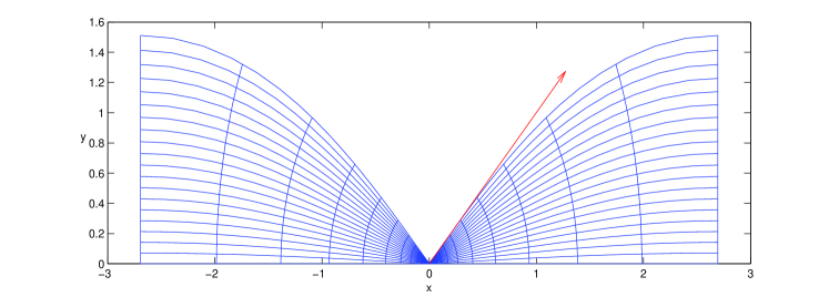
We consider two-dimensional conduction through a symmetric periodic glass layer of wave-length that has varying thickness, , driven by an applied electric potential difference . The glass layer has average thickness and minimum thickness . We focus on a system where a glass layer separates a silver crystallite from the silver electrode. We want to investigate the short circuiting of the current through thinner regions of the glass layer. We therefore consider two different generic cases for the variation of the thickness of the glass layer: (i) the radius of curvature, , of the silver electrode is much larger than the minimum thickness of the glass layer , which implies the thickness of the glass layer varies slowly, see figure 2(a); (ii) the radius of curvature so that the domain appears wedge-like and the thickness of the glass layer varies quickly, see figure 2(b). In the latter case we find it more convenient to parametrise the domain by the angle from the horizontal, .
2.2 Nondimensional model
To formulate the mathematical model we make the following assumptions; see [7] for further details.
-
1.
Charge is predominantly carried by electrons and not holes.
-
2.
The system is in quasi-steady state.
-
3.
The flux of electrons results from combination of drift and diffusion.
-
4.
The electric potential satisfies Poisson’s equation.
We then follow the same nondimensionalisation as in [7] to obtain the following governing equations
| (1) | ||||
| (2) | ||||
| (3) |
where is the density of free electrons, and the boundary conditions are
| (4) |
where we assume periodic boundary conditions in the -direction. A schematic of the domain and the boundary conditions is given in figure 3. The dimensionless parameters are
| (5) |
where is the nondimensional length of the glass layer and can be thought of as the aspect ratio (), is the average thickness of the glass layer, is the Debye length, is the absolute permittivity, is Boltzmann’s constant, is absolute temperature, is the electron density at the silver electrode interface and is the charge on an electron. We expect the Debye length typically to be small compared with the average glass layer thickness, and hence the parameter to be small. It is when the Debye length is small compared with the average glass layer thickness that the short-circuting effects investigated are especially evident. We only consider cases where since this corresponds to electron flow into the silver electrode.
2.3 Model outputs
From the solution of the mathematical model there are a number of different quantities we will calculate to gain greater insight into the electron transport across the glass layer. Firstly, we will determine the average current density through the glass layer which is given by
| (6) |
the total current is given by . To investigate qualitatively the short circuiting of the current through thinner glass layer regions we calculate: (i) the electron trajectories through the glass layer; (ii) the normalised cumulative current
| (7) |
The deviation of the function from linear indicates focusing of the current.
Finally, we define the effective resistance of the glass layer as
| (8) |
3 Transformation to rectangular domain
3.1 Introduction
In this paper we solve (1)–(4) using a spectral numerical method. The numerical solution is facilitated by mapping the domain to a rectangle. In this section we outline two alternative mapping techniques: a hodograph formulation, particularly suitable for investigating the slowly varying domain (figure 2(a)) and a conformal map formulation [3], ideal for investigating the wedge domain (figure 2(b)).
3.2 Hodograph transformation
Equation (1) implies the existence of a streamfunction such that
| (9) |
The introduction of the electro-chemical potential enables us to write (2) as
| (10) |
Now by considering the boundary conditions (4), we observe that the change of independent variables from , maps the solution domain onto the rectangle . The Jacobian of the transformation is given by
| (11) |
Now by inverting the relations (10) we find that
| (12) |
and hence
| (13) |
To formulate our problem in the Hodograph plane we want to write (3) in terms of and . We use the chain rule to find that
| (14) | ||||
| (15) |
Substituting (14) and (15) into (3), and making use of (10) and (11) we obtain
| (16) |
Finally, substituting (13) into (16) and eliminating from (12) we find the governing equations in the hodograph plane:
| (17) | ||||
| (18) |
with boundary conditions
| (19) | ||||||||||
| (20) |
A schematic of the hodograph plane and boundary conditions is shown in figure 4. We note that in this formulation the method has become semi-inverse in nature as we now specify the total current and solve for the length of the domain . We also specify the function that determines indirectly the shape of the top surface in the physical plane, .
To plot our results in the physical plane we calculate :
| (21) |
In the hodograph plane the length of the physical domain is now an output and given by
| (22) |
should be independent of and any variation in over the range of is due to numerical error. The electron trajectories are easily found as curves of constant . Finally, the cumulative current is found by inverting the function to determine .
3.3 Conformal mapping
3.3.1 Transformed problem
As an alternative to the hodograph transformation described above, suppose instead that the rectangle is mapped onto the physical domain of interest by a conformal transformation
| (23) |
Application of (23) to (1)–(3) gives the following equations in the transformed frame:
| (24) | ||||
| (25) |
where , and the boundary conditions (4) become
| (26) |
A schematic of the domain and boundary conditions is shown in figure 5.
The height of the rectangular domain is chosen to ensure that the nondimensional average thickness of the glass layer is equal to , that is,
| (27) |
where is the maximum value that takes in the plane.
The calculation of the average current density is achieved using the relation
| (28) |
where . To obtain the electron trajectories, we solve the equations
| (29) |
using the overloaded ode45 function in Chebfun and then map back to the physical domain. Finally, the cumulative current plots can be produced by noting the relation
| (30) |
and using the overloaded cumsum command in Chebfun.
3.3.2 Mapping function
For a given physical domain a numerical conformal map can be constructed by making use of the Schwarz-Christoffel transformation. However, to explore domains with a wedge-like geometry, we use the following mapping function, see Hale & Tee [17]:
| (31) |
where denotes the complete elliptic integral of the first kind; and are Jacobi elliptic functions. The suppressed argument of , and is defined by
| (32) |
Hence the map (31) depends on one parameter in addition to the length of the periodic domain.
The function is univalent on the rectangle provided , where
| (33) |
As shown in figure 6, the function (31) maps the rectangle in the -plane to a strip in the -plane, minus a branch cut from to . For , the line is mapped to a periodic curved upper surface that is wrapped around the branch cut. Moreover, when and are small, the geometry approaches that of a rounded wedge which narrowly avoids intersecting the lower surface at . In the limit as , we find that
| (34) |
The parameters and may thus be related to the asymptotic minimum layer thickness and wedge angle using the formulae
| (35) |
and the local geometry is that of a hyperbola, with
| (36) |
The use of the analytic conformal map, (31), rather than a numerical Schwarz-Christoffel map, reduces computational effort and allows easy parameterisation of a range of wedge-like domains.
3.4 Summary
We have formulated two different techniques for mapping the governing equations to a rectangular domain. These approaches each have advantages and disadvantages and are appropriate for treating different domains. The conformal map formulation is straightforward to apply and, if an analytic map can be found as shown above, allows for the easy manipulation of the domain shape. Of course in general the Schwarz-Christoffel toolbox can be used to obtain numerical mapping functions, although this adds computational effort [14]. The calculation of the electron trajectories and cumulative current also requires significant additional numerical calculations. In contrast, the hodograph plane formulation makes it easy to determine these desired quantities. In theory, the hodograph plane formulation allows the treatment of a wide range of domain shapes. However, unless a priori knowledge of an appropriate is known, it is difficult to reproduce a given domain.
4 Numerical method
4.1 Introduction
Via either of the transformations described in Section 3, we may henceforth assume that the governing equations are posed on a rectangular domain making them more suitable for numerical solution. The numerical method we will use is a 2D spectral method. The basis of spectral methods is to take discrete data on a grid, interpolate this data with a global function and then evaluate the derivative of the interpolating function on the grid. Given a periodic problem one would typically use trigonometric interpolants on equispaced points, and given a non-periodic problem it is commonplace to use Chebyshev polynomial interpolants on Chebyshev spaced points [40]. Both formulations laid out in Section 3 are periodic in one direction and non-periodic in the other, and we will therefore choose the appropriate interpolants in each direction accordingly.
4.2 Demonstration of implementation
We will give a detailed description of how the numerical method is implemented on the conformally mapped problem, (24)–(26); this numerical method can be applied to analagous nonlinear elliptic equations in a rectangle and therefore exactly the same methodology is used for the hodograph plane formulation. To apply Newton’s method we calculate the Fréchet derivatives of the governing equations with respect to the two unknowns and :
| (37) | ||||
| (38) | ||||
| (39) | ||||
| (40) |
Given an approximation to the solution, we therefore calculate an improved approximation , where , are the updates and is the damping parameter that increases the chance of an initial guess converging to a solution [6]. The updates satisfy the linear partial differential equations
| (41) |
We ensure that the initial guess satisfies the boundary conditions in the direction so we can specify homogenous boundary conditions for the update . We also specify periodic boundary conditions in the direction, i.e.
| (42) |
The successive approximations are calculated repeatedly until the update .
To solve (41), (42) numerically we convert the variables , , , and from 2D continuous objects into vectors on the domain discretised with equispaced points in the periodic direction and Chebyshev spaced points in the non-periodic direction. To turn the 2D grid into a vector, we index from the bottom left hand corner as illustrated in figure 7.
To write the system (41) as a matrix equation we introduce the notation:
| (43) | ||||
| a square matrix with the variable on its | ||||
| diagonal. | (44) |
We make use of the Schwarz-Christoffel toolbox [14] and take the differentiation matrices from the MATLAB dmsuite [45], where is a Fourier differentiation matrix and is a Chebyshev differentiation matrix. Using this notation, (41) becomes
| (45) |
where denotes element-wise multiplication and the boundary conditions are
| (46) |
Boundary conditions in the direction are not needed as we use Fourier differentiation matrices that assume periodicity. To apply the boundary conditions (46) we replace rows in the matrices in (45) so that the relevant elements of and are selected and set to zero. We first solve the problem in using Chebfun and then extend this into the second dimension to create the initial guess. The system (45) is then solved using damped Newton iteration where the damping parameter is calculated using the algorithm given in the appendix of [6].
Finally, to obtain the variables and in the transformed frame we first interpolate the periodic points to Chebyshev points using fourint.m [45] and then use Chebfun to create chebfun objects of and . This enables us to access the wide range of functionality built into Chebfun for further analysis of the results.
4.3 Validation
We now validate our numerical method by investigating its convergence for both the conformal map formulation and the hodograph plane formulation for the same test problem. The domain considered is produced using (31) with , , and and is shown in figure 8. We also let and in our numerical test. We are able to use the results from the conformal map formulation to determine the corresponding and in the hodograph plane formulation.
To examine the convergence of the numerical method we fix the number of points in one direction and vary the number of points in the other and then observe how the integrated quantity converges by considering the quantities
| (47) |
for the conformal map approach, and
| (48) |
for the hodograph approach.
Tables 2(a)–2(d) show the results of our convergence tests and clearly demonstrate that both numerical methods rapidly converge to the same solution. We observe that the error decreases exponentially with the number of discretisation points, as expected for a spectral method. It is evident that fewer points are required in the conformal map formulation than the hodograph plane formulation to achieve the same accuracy. We believe that this occurs because the solutions for and are smoother in the conformal mapping plane than in the hodograph plane. Additionally, we find in the hodograph plane formulation the numerical method is sensitive to the smoothness of the function .
4.4 Example numerical solutions
4.4.1 Smooth domain
We consider the domain shown in figure 9 where , , the radius of curvature at is and
| (49) |
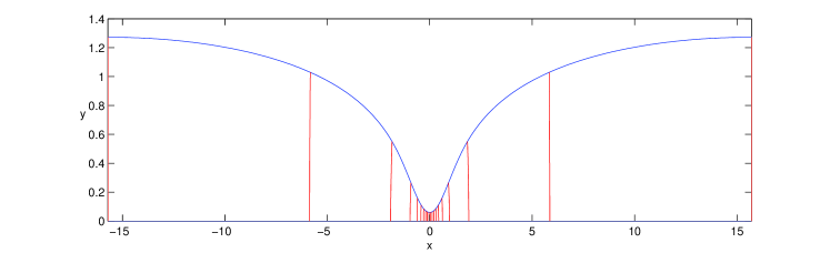
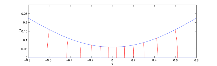
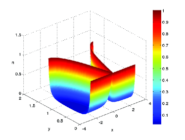
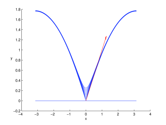
in the central region, where the edges are patched to polynomials (this choice will be justified below in Section 5.1). For illustration, we set and , since we expect the normalised Debye length to be small in practice. In figure 10 we plot the numerical solutions for and . We observe boundary layers at the two surfaces of the glass layer away from the minimum . Near the minimum, however, we see that while varies approximately linearly across the layer. Both of these structures were found by Black et al. [7] in limiting one-dimensional solutions. The presence of the large electron density in the central region means we expect the majority of the current to be collected there. This is visible in figure 11 where the electron trajectories are plotted with equal current between each trajectory and are largely concentrated around . Also figure 11(b) displays the quasi-1D nature of the solution near , as the electron trajectories have little -variation. This quasi-1D behaviour is due to the slowly varying top surface: note the different axes scalings in figure 9.
The effective resistance of the domain in figure 9 with and is . On the otherhand, with and , a uniform glass layer with the same average thickness has an effective resistance . Therefore the short circuiting causes a reduction in the net resistance by a factor of approximately .
4.4.2 Wedge-like domain
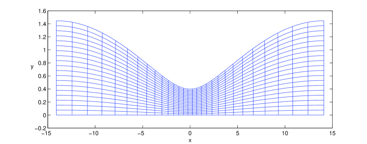
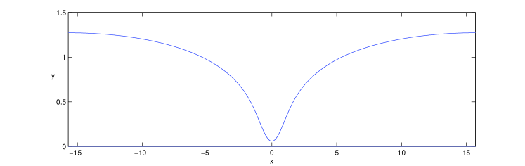
We will now analyse a wedge domain where we let , , , and . The corresponding parameter values in the mapping function (31) are and . The domain is shown in figure 12.
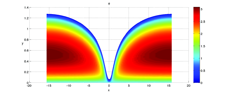
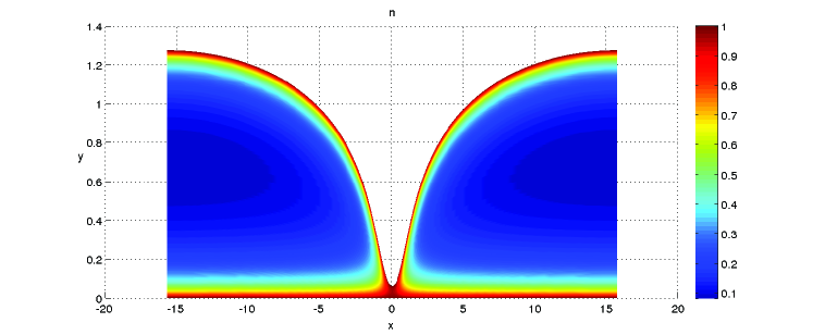
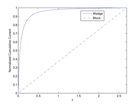
In figure 13 the numerical solutions for and are plotted. These figures exhibit the same general features as figures 10 and 10, with a boundary layer structure away from and a region of high current density near . The short circuiting of the current through the thinner region is demonstrated by plotting the cumulative current distribution in figure 14. We observe that over of the current is collected within a neighbourhood of . In figure 14 we include the corresponding curve for a glass layer with constant thickness for a reference. In general, the more concave the normalised cumulative current is, the more the current is short-circuiting through the region around .
Finally, the effective resistance for the domain shown in figure 12, with and , is . For comparison, with the same values for and , the resistance of a uniform glass layer with the same average thickness is . This example illustrates the dramatic effect that nonuniform thickness may have on the net resistance: here the short-circuiting of the current causes a reduction in the resistance by a factor of . The increased difference between these values when compared with those in Section 4.4.1 is mainly due to the smaller values of and used.
4.5 Summary
In this section we have demonstrated the implementation of a new numerical method that can be used to solve for the electron density and electric potential in both the conformal mapping and the hodograph plane formulations. The method has been validated for both implementations, with exponential convergence evident. The agreement that we find between the different implementations for the solution of the same problem gives high confidence in both methods. We have considered some example cases and found that short-circuiting through the thinner regions of the glass layer causes a significant reduction in resistance when compared to a constant thickness domain. This behaviour motivates us to seek asymptotic expressions for the average current density as the minimum thickness . We will see that the solution structure depends crucially on whether the local behaviour is “slowly varying” or “wedge-like”.
5 Asymptotic analysis
5.1 Slowly varying domain
We now calculate an approximation to the average current density in the limit where the local radius of curvature, . It follows that the thickness profile near the minimum is indeed slowly varying, with local aspect ratio . We focus on this region by performing the rescalings
| (50) |
Then the current density takes the form and, to lowest order in , the problem (1)–(4) is quasi-one-dimensional, i.e.
| (51) |
subject to the boundary conditions
| (52) |
The problem now depends on only parametrically, and the transformations
| (53) |
reduce (51)–(5.1) to the corresponding purely one-dimensional problem
| (54) |
| (55) |
which was analysed in detail in [7]. Let us denote the solution for the current in this one-dimensional problem by .
By reversing the transformations carried out above, we deduce that the net resistance of the layer in the limit is approximated by
| (56) |
The function is in general determined numerically; however analytic approximations were found in various limiting cases in [7]. In particular, in the limit , the layer acts as a resistor with . If , i.e. the minimum thickness is smaller than the Debye length, we may therefore use to approximate (56) as
| (57) |
Now we wish to test the approximation (57) against our numerical results. As noted in Section 3.4, the hodograph formulation is most useful when a priori knowledge of an appropriate is known. However, it requires us to pose the relation , where the function is indirectly related to the upper surface profile . Here we can use the asymptotic behaviour of the solution found above to determine the corresponding local behaviour of near the minimum thickness, namely by making use of
| (58) |
we determine
| (59) |
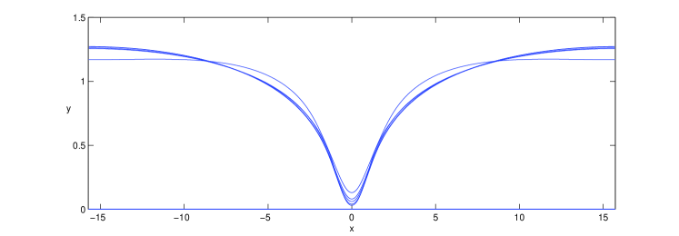
Note that we expect as . Evidently (59) breaks down as and . In any case, the numerical scheme requires to be periodic, which we achieve by patching the edges of (59) to suitable polynomials. A selection of domains used for comparison to our asymptotic expression is shown in figure 15. As in the conformal map formulation the average thickness of the glass layer is always equal to .
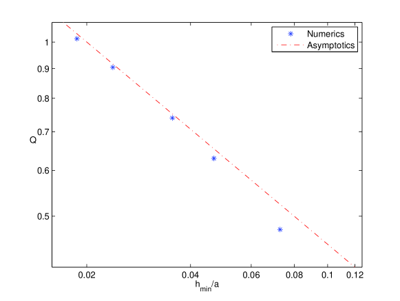
In figure 16 we demonstrate that the asymptotic expression (57) gives an excellent approximation to the results of numerical simulations for the average current density as . This analysis accentuates how short-circuiting through any thin spots in the glass layer may dominate the overall flux. However, the approximation (57) rests on the assumption that , and will therefore fail if the curvature of the glass surface is too large in the neighbourhood of the minimum. To describe the local behaviour in such sharp “wedge-like” domains, a different asymptotic approach is required, as will be demonstrated below.
5.2 Wedge-like domain
5.2.1 Introduction
In this section we investigate the behaviour of the average current density in a wedge-like domain, with as . If we naively set , we are left with the “outer” problem illustrated in figure 17(a): the glass layer thickness reaches zero with a corner singularity at (without loss of generality) . The problem is regularised over a small region in which , as illustrated in figure 17(b). In this “inner” problem, the glass layer has unit minimum thickness and approaches a wedge shape as . Below we will analyse the inner and outer problems and match them asymptotically to obtain an approximation for the net flux through the layer.
5.2.2 Outer problem
The outer problem, namely the full governing equations (1)–(3) with the boundary conditions shown in figure 17(a), requires numerical solution in general. For matching purposes, we only require the asymptotic behaviour of the solution as , which is easily found to be
| (60) |
where are plane polar coordinates.
5.2.3 Inner problem
In the inner problem we scale and let while expanding the solution as
| (61) |
We find that and satisfies Laplace’s equation
| (62) |
subject to the boundary conditions shown in figure 17(b). In principle, this problem is easily solved by conformal mapping. Assuming that the inner geometry shown in figure 17(b) is the image of a strip under the conformal map
| (63) |
then the solution in the strip is given by
| (64) |
Here we have assumed that maps the real line to itself and also fixes the points , and . For example, the locally hyperbolic upper surface described by (34)–(36) corresponds to the mapping function
| (65) |
5.2.4 Average current density approximation
Now we find the leading-order average current density through the layer by integrating over the inner and outer regions. Assuming symmetry about the -axis, we have
| (66) |
where is assumed to satisfy , and , are the contributions from the outer and inner regions respectively. We know from (60) that the outer integral diverges logarithmically as and, by subtracting the singular part, we obtain
| (67) |
For the inner contribution, we may perform the integral in the -plane to obtain
| (68) |
where is the point on the -axis corresponding to , i.e.
| (69) |
Now, from the wedge geometry, we must have as , where is a real constant that depends on the detailed inner geometry; for example, for the mapping function (65). Hence the leading-order inner integral is given by
| (70) |
5.2.5 Comparison between asymptotics and numerics
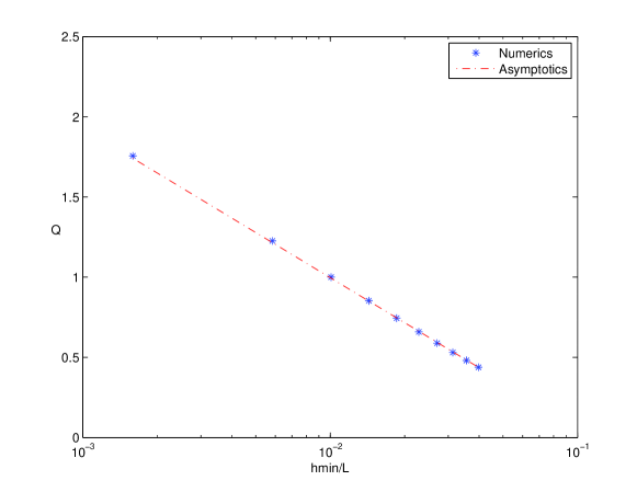
To validate our asymptotics we perform a sequence of simulations that fix the constant . We therefore consider a range of domains with the same and , as shown in figure 18, and take and in each simulation. We must then relax the condition for the average thickness to be . The results are plotted in the linear-log plot in figure 19 where it is evident the asymptotic expression (71) gives a very good approximation for the average current density as . In principle, one could calculate by solving the outer problem but we curve-fit to find for this particular geometry. Similarly to Section (5.1) the analysis demonstrates how the overall flux is dominated by short circuiting through thinner regions.
6 Conclusion and discussion
In this paper we extend to two dimensions the mathematical model from [7] for steady electron transport through a glass layer between two electrodes. We maintain many of the same modelling assumptions: that the charge is predominantly carried by electrons, that the electron flow is governed by drift and diffusion, and that the electron densities are known either side of the glass layer. The analysis focuses on the short-circuiting of current through thinner regions of the glass layer, and we present a spectral numerical method to solve the model once it has been mapped onto a rectangular domain.
We make use of two different mapping techniques; which approach is preferable depends on the geometry under consideration and the questions one wishes to answer. In both cases, we validate the numerical method through its exponentially rapid convergence and its ability to produce insightful results such as the electron trajectories and the normalised cumulative current. In considering nonuniform domains, the numerical results demonstrate how the current short-circuits through thinner regions of the glass. Consequently, the effective resistance is significantly lower than comparable domains with constant glass layer thickness.
We use the numerical simulations to inform asymptotic calculations conducted on domains with small minimum thickness . We consider two canonical local geometries. First we suppose that the thickness profile is smooth, and the local layer thickness is therefore “slowly varying” as . In this limit, we find that the current through the layer diverges like , where is the local radius of curvature. The second regime considered is where , so that the local behaviour of the surface is “wedge-like”. In this latter case, we find a weaker logarithmic divergence of the current as . Both predictions are found to agree well with full numerical calculations.
The generalisation of our model into two dimensions is well warranted. In experimental images of the front contact (see for example [24, 25]), the glass layer is observed to vary greatly in thickness, from nm–m. However, some of our modelling assumptions should be readdressed, such as the neglect of holes and the simplified boundary conditions (discussed in more detail in [7]). The presence of a positive charged species would require another transport law and the addition of a thermodynamic equilibrium law; an example is given in [33]. A physical process we have not considered is that silver ions could intercalate and transport across the glass layer leading to a dendritic short circuit. Additionally, we note that, in the limit as the glass layer becomes very thin, the validity of the continuum model must eventually be questioned. Preliminary work suggests that below nm quantum tunnelling effects start to play a role in determining the resistance of the glass layer. These quantum effects can be modelled through a modified drift-diffusion model, with a higher order derivative term added to (2); see, for example [2, 13, 32]. Finally, it is well known that at very high electric fields the drift-diffusion equations lose their validity [39]. As the glass layer thickness decreases below nm, sufficiently high fields could be present at relatively moderate potential differences. In these high field limits it is possible instead to use Monte Carlo methods to simulate charge transport; see [20].
Our model could be the building block for studying other, related, physical problems with some modification. For example, in electrochemical thin films where there are multiple charged species moving under drift and diffusion, more complicated boundary conditions such as Butler-Volmer would be needed to describe reaction kinetics for electron transfer [4, 8, 12].
The dominant conduction mechanism for electron transport across the glass layer is under fierce debate and mathematical models such as the one explored in this paper can help with hypothesis testing. In particular, our study has shown that the geometry of the glass layer makes significant difference to electron transport and hence performance of the photovoltaic cell.
Acknowledgements
The authors are grateful to Á. Birkisson, N. Hale, C. P. Please and the employees of DuPont (UK) Ltd for many useful discussions. This work is supported by EPSRC and DuPont (UK) Ltd.
References
- [1] T. Adachi, A. Yoshii, and T. Sudo. Two-dimensional semiconductor analysis using finite-element method. IEEE Trans. Electron Devices, 26(7):1026–1031, 1979.
- [2] M. G. Ancona and H. F. Tiersten. Macroscopic physics of the silicon inversion layer. Phys. Rev. B, 35(15):7959–7965, 1987.
- [3] M. Z. Bazant. Conformal mapping of some non-harmonic functions in transport theory. Proc. R. Soc. Lond. Ser. A Math. Phys. Eng. Sci., 460:1433–1452, 2004.
- [4] M. Z. Bazant, K. T. Chu, and B. J. Bayly. Current-voltage relations for electrochemical thin films. SIAM J. Appl. Math., 65(5):1463–1484, 2005.
- [5] P. M. Biesheuvel and M. Z. Bazant. Nonlinear dynamics of capacitive charging and desalination by porous electrodes. Phys. Rev. E, 81(3):031502, 2010.
- [6] Á. Birkisson and T. A. Driscoll. Automatic Fréchet differentiation for the numerical solution of boundary-value problems. ACM Trans. Math. Software, 38(4):26, 2012.
- [7] J. P. Black, C. J. W. Breward, P. D. Howell, and R. J. S. Young. Mathematical modeling of contact resistance in silicon photovoltaic cells. SIAM J. Appl. Math., 73(5):1906–1925, 2013.
- [8] A. Bonnefont, F. Argoul, and M. Z. Bazant. Analysis of diffuse-layer effects on time-dependent interfacial kinetics. J. Electroanal. Chem., 500(1):52–61, 2001.
- [9] D. Brinkman, K. Fellner, P. A. Markowich, and M.-T. Wolfram. A drift–diffusion–reaction model for excitonic photovoltaic bilayers: Asymptotic analysis and a 2d hdg finite element scheme. Math. Models Methods Appl. Sci., 23(05):839–872, 2013.
- [10] E. Cabrera, S. Olibet, J. Glatz-Reichenbach, R. Kopecek, D. Reinke, and G. Schubert. Current transport in thick film Ag metallization: Direct contacts at silicon pyramid tips? Energy Procedia, 8:540–545, 2011.
- [11] L. K. Cheng, L. Liang, and Z. Li. Nano-Ag colloids tunneling mechanism for current conduction in front contact of crystalline si solar cells. In Proceedings of the 34th IEEE Photovoltaics Specialists Conference (PVSEC), pages 2344–2348, Philadelphia, PA, 2009.
- [12] K. T. Chu and M. Z. Bazant. Electrochemical thin films at and above the classical limiting current. SIAM J. Appl. Math., 65(5):1485–1505, 2005.
- [13] E. Cumberbatch, S. Uno, and H. Abebe. Nano-scale mosfet device modelling with quantum mechanical effects. European J. Appl. Math., 17(4):465–489, 2006.
- [14] T. A. Driscoll. Algorithm 843: improvements to the Schwarz-Christoffel toolbox for MATLAB. ACM Trans. Math. Software, 31(2):239–251, 2005.
- [15] J. M. Foster, J. Kirkpatrick, and G. Richardson. Asymptotic and numerical prediction of current-voltage curves for an organic bilayer solar cell under varying illumination and comparison to the Shockley equivalent circuit. J. Appl. Phys., 114(10):104501, 2013.
- [16] H. K. Gummel. A self-consistent iterative scheme for one-dimensional steady state transistor calculations. IEEE Trans. Electron Devices, 11(10):455–465, 1964.
- [17] N. Hale and T. W. Tee. Conformal maps to multiply slit domains and applications. SIAM J. Sci. Comput., 31(4):3195–3215, 2009.
- [18] K.-K. Hong, S.-B. Cho, J. S. You, J.-W. Jeong, S.-M. Bea, and J.-Y. Huh. Mechanism for the formation of Ag crystallites in the Ag thick-film contacts of crystalline Si solar cells. Sol. Energy Mater. Sol. Cells, 93(6):898–904, 2009.
- [19] A. S. Ionkin, B. M. Fish, Z. R. Li, M. Lewittes, P. D. Soper, J. G. Pepin, and A. F. Carroll. Screen-printed silver pastes with metallic nano-zinc and nano-zinc alloys for crystalline silicon photovoltaic cells. ACS Appl. Mater. Inter., 3(2):606–611, 2011.
- [20] C. Jacoboni and P. Lugli. The Monte Carlo method for semiconductor device simulation, volume 3. Springer, 1989.
- [21] M.-I. Jeong, S.-E. Park, D.-H. Kim, J.-S. Lee, Y.-C. Park, K.-S. Ahn, and C.-J. Choi. Transmission electron microscope study of screen-printed Ag contacts on crystalline Si solar cells. J. Electrochem. Soc., 157(10):H934–H936, 2010.
- [22] S. Kontermann, R. Preu, and G. Willeke. Calculating the specific contact resistance from the nanostructure at the interface of silver thick film contacts on n-type silicon. Appl. Phys. Lett., 99(11):111905, 2011.
- [23] S. Kontermann, G. Willeke, and J. Bauer. Electronic properties of nanoscale silver crystals at the interface of silver thick film contacts on n-type silicon. Appl. Phys. Lett., 97(19):191910, 2010.
- [24] Z. G. Li, L. Liang, and L. K. Cheng. Electron microscopy study of front-side Ag contact in crystalline Si solar cells. J. Appl. Phys., 105(6):066102, 2009.
- [25] Z. G. Li, L. Liang, A. S. Ionkin, B. M. Fish, M. E. Lewittes, L. K. Cheng, and K. R. Mikeska. Microstructural comparison of silicon solar cells’ front-side Ag contact and the evolution of current conduction mechanisms. J. Appl. Phys., 110(7):074304, 2011.
- [26] C.-H. Lin, S.-Y. Tsai, S.-P. Hsu, and M.-H. Hsieh. Investigation of Ag-bulk/glassy-phase/Si heterostructures of printed Ag contacts on crystalline Si solar cells. Sol. Energy Mater. Sol. Cells, 92(9):1011–1015, 2008.
- [27] P. A. Markowich. A singular perturbation analysis of the fundamental semiconductor device equations. SIAM J. Appl. Math., 44(5):896–928, 1984.
- [28] P. A. Markowich, C. A. Ringhofer, and C. Schmeiser. An asymptotic analysis of one-dimensional models of semiconductor devices. IMA J. Appl. Math., 37(1):1–24, 1986.
- [29] P. A. Markowich and C. S. Schmeiser. Uniform asymptotic representation of solutions of the basic semiconductor-device equations. IMA J. Appl. Math., 36(1):43–57, 1986.
- [30] R. J. Mortimer. Electrochromic materials. Chem. Soc. Rev., 26(3):147–156, 1997.
- [31] W. D. Murphy, Manzanares J. A., S. Mafé, and H. Reiss. A numerical study of the equilibrium and nonequilibrium diffuse double layer in electrochemical cells. J. Phys. Chem., 96(24):9983–9991, 1992.
- [32] R. Pinnau. A review on the quantum drift diffusion model. Transport Theory Statist. Phys., 31(4-6):367–395, 2002.
- [33] C. P. Please. An analysis of semiconductor p-n junctions. IMA J. Appl. Math., 28(3):301–318, 1982.
- [34] G. Richardson, C. P. Please, J. M. Foster, and J. Kirkpatrick. Asymptotic solution of a model for bilayer organic diodes and solar cells. SIAM J. Appl. Math., 72(6):1792–1817, 2012.
- [35] G. Schubert. Thick Film Metallisation of Crystalline Silicon Solar Cells. PhD thesis, University of Konstanz, 2006.
- [36] J. W. Slotboom. Iteratics scheme for 1- and 2- dimensional DC-transistor simulation. Electron. Lett., 5(26):677–678, 1969.
- [37] J. W. Slotboom. Computer-aided two-dimensional analysis of bipolar transistors. IEEE Trans. Electron Devices, 20(8):669–679, 1973.
- [38] C. M. Snowden. Semiconductor device modelling. Rep. Prog. Phys., 48(2):223–275, 1985.
- [39] S. M. Sze and K. K. Ng. Physics of semiconductor devices. John Wiley & Sons, 2006.
- [40] L. N. Trefethen. Spectral methods in MATLAB. SIAM, Philadelphia, 2000.
- [41] L. N. Trefethen. Approximation Theory and Approximation Practice. SIAM, Philadelphia, 2013.
- [42] L. N. Trefethen et al. Chebfun Version 5.0, 2014. http://www.chebfun.org.
- [43] M. van Soestbergen, A. Mavinkurve, R. T. H. Rongen, K. M. B. Jansen, L. J. Ernst, and G. Q. Zhang. Theory of aluminum metallization corrosion in microelectronics. Electrochim. Acta, 55(19):5459, 2010.
- [44] M. Ward, F. Odeh, and D. Cohen. Asymptotic methods for metal oxide semiconductor field effect transistor modeling. SIAM J. Appl. Math., 50(4):1099–1125, 1990.
- [45] J. A. C. Weideman and S. C. Reddy. A MATLAB differentiation matrix suite. ACM Trans. Math. Software, 26(4):465–519, 2000.