Theory of carrier transport in graphene double-layer structure
with carrier imbalance
Abstract
The carrier mobility of a graphene double-layer system is evaluated on the basis of the Boltzmann transport theory. In this system, two graphene layers are separated by a dielectric barrier layer. We focus on the cases in which there is carrier imbalance between the two layers. It is found that the mobility can be improved by controlling the carrier density polarization between the two layers if we choose an appropriate dielectric environment.
1 Introduction
Graphene, a one atomic-thickness carbon sheet, has attracted much interest owing to its unique electronic properties such as the half-integer Hall effect and ultra -high mobility. The electronic states of graphene near the Fermi energy are well described by the two-dimensional massless Dirac equation.
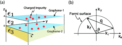
Recently, electronic devices composed of graphene and other atomically thin materials have also been proposed [1, 2, 3, 4, 5]. One such system is the graphene double-layer system, in which two graphene layers are separated by a thin dielectric, as shown in Fig. 1(a) [2, 3, 4, 5, 6, 7, 8]. Since the interlayer interaction can be controlled by adjusting the interlayer distance, the GDLS has been considered to be a good platform for studying the exciton superfluidity [9, 10, 11], Coulomb drag effect [10, 12] and plasmon mode [15, 14, 13]. The Coulomb drag effect was demonstrated using Al2O3[2] and h-BN [3, 4, 17, 18, 16] as middle dielectrics. Theoretical analysis of the device performance of GDLS has only just begun.
Carrier mobility is one of the key benchmarks of device performance because it determines the power dissipation and switching speed of the device. Recent theory suggests improving carrier mobility by placing a high- overlayer on a semiconductor nanostructure, which leads to the weakening of Coulomb scattering due to the screening effect [19, 20]. Indeed, several electronic transport measurements of graphene or atomically -thin material have successfully revealed mobility enhancement via change in the dielectric environment [21, 22, 23, 24, 25]. In our previous paper, we have constructed a formulation for evaluating the dependence of the interlayer distance and the effect of the dielectric environment on the charged-impurity-limited carrier mobility of the GDLS on the basis of the Boltzmann transport theory.
We have pointed out that the carrier mobility of GDLS strongly depends on the dielectric constant of the barrier layer when the interlayer distance becomes larger than the inverse of the Fermi wave vector [26]. However, we have considered only the case in which the carrier concentrations at each layer are equivalent (), and have neglected carrier density polarization, for simplicity. Since the carrier density at each layer can be controlled by adjusting the gate voltage in the experiments, it is necessary to develop a theory that takes carrier imbalance into account.
In this study, we focus on the case in which there is carrier imbalance. We evaluate the effect of carrier density polarization (denoted by ) on the charged-impurity-limited carrier mobility in the GDLS by extending our previously -reported formulation. It is found that the carrier density polarization dependence of the carrier mobility is affected by the surrounding dielectrics and interlayer distance. The carrier mobility in the presence of carrier density imbalance strongly depends on the interlayer distance if we set particular constants of the dielectric environment. Our result offers appropriate ranges of the carrier polarization and dielectric constant of the surrounding dielectrics to improve the charged-impurity limited mobility of GDLS.
2 Model and formulation
Figure 1(a) shows a schematic of the GDLS, in which two graphene layers are separated by three different dielectrics, i.e., and . We assume that the two graphene layers are coupled only through the Coulomb interaction between the charged impurities and carriers. The Hamiltonian can be written as
| (1) | ||||
where () is the creation (annihilation) operator for an electron with the wave vector (,) and the pseudospin on the -th graphene layer. Here, eVÅ is the band parameter. and are the Pauli spin matrices for pseudospin; are pseudospin labels for describing the sublattice of the honeycomb lattice. is the area of each graphene layer. denotes the Fourier component of the screened Coulomb potential, which depends on the interlayer distance , and includes the effect of the Coulomb interaction between carriers on each graphene layer through the polarization function [33]. is the particle density of random impurities on the -th graphene layer having the total number of impurities . represents the position of the impurities on the -th layer.

The inverse of the carrier mobility can be described by [29, 28]. Here, () is the contribution of the intralayer scattering rate of the first (second) graphene layer, and and are the contributions of interlayer scattering. According to the semiclassical Boltzmann theory, the inverse of the each contribution of carrier mobility is given by
| (2) |
where is the impurity concentration on the first (second) graphene layer. The impurity concentration for interlayer scattering is given as the average of two layers . For simplicity, we assume that the impurity concentration at each layer is equivalent and that the Fermi level of both graphene layers lies in the conduction band. is the density of states of single-layer graphene with owing to the valley and spin degeneracy. is the scattering angle, and is the scattering wave vector on the circular two-dimensional Fermi surface, as shown in Fig. 1(b). The Fermi wave number on each graphene layer is given as . Note that the last -dependent factor also contains the phase of the wave function of graphene [33, 29]. The structural parameter such as the interlayer distance and scattering potential due to charged impurities are included in the screened potentials .
Here, we briefly explain the derivation of the screened Coulomb potential from the unscreened one . The analytical expression of the unscreened Coulomb potentials of the GDLS can be derived using the image charge method [27, 19, 25]. For this system, we need to consider an infinite series of point image charges arising from two interfaces at and shown in Fig. 1(a), where two types of dielectrics are spanned by a graphene layer. The resulting unscreened Coulomb potentials are given as
| (3) | ||||
| (4) | ||||
| (5) | ||||
| (6) |
Here and are the intralayer Coulomb interactions on the first and second graphene layers, respectively. and are the interlayer Coulomb interactions, and we define
| (7) |
The above potentials have been used in the context of the superfluid magnetoexitons [9] and plasmon mode [14, 15] of the GDLS. The above expressions indicate that the parameter () determines the screening behavior and the strength of the interlayer Coulomb interaction.
The screened Coulomb potentials are described by the random phase approximation (RPA) as
| (8) |
where
Here, is the static polarization function of the first (second) graphene layer [28, 29]. The static polarization is written as
| (9) |
where and are given as
| (10) |
From Eq. (8), the effective interactions are obtained as
| (11) | ||||
| (12) |
| (13) | ||||
| (14) |
where the intralayer interactions and , and the interlayer interactions and are defined in Eqs. (3)-(6), respectively. Here, the dielectric function is defined as
| (15) |
By combining Eqs. (11)-(15), we can evaluate the carrier mobility of GDLS in the presence of an imbalance in the concentration between two graphene layers, i.e., .


3 Results and discussion
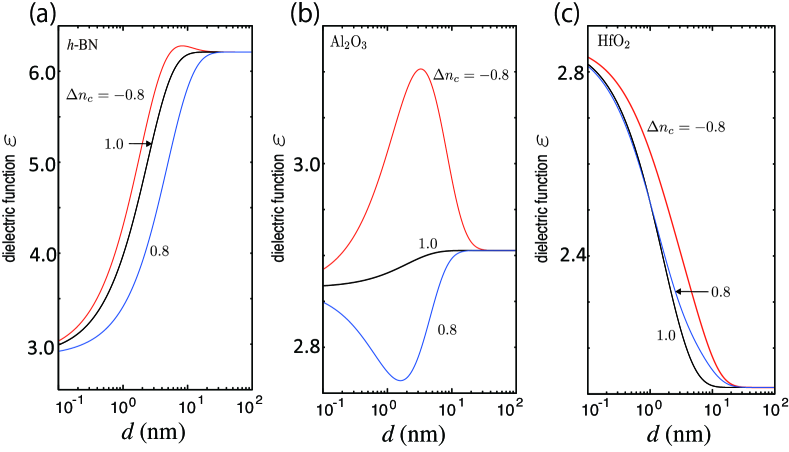
We first investigated the dependence of the dielectric function Eq. (15) on the interlayer distance and carrier density polarization. Here, we define the carrier density polarization as , and fix the total carrier concentration at . When the carriers are only in the first (second) layer, . In the case of in which the two layers have identical carrier densities, the dielectric function captures the screening effect of scattering potentials due to charged impurities. In order to see the role of the middle dielectric layer, we assume the dielectric constants for the top and bottom layers as and , respectively, and consider three different dielectrics as the middle layer, i.e., h-BN, Al2O3, and . Their dielectric constants are , , and , respectively[30, 31, 32].
Figure 2 shows the dependences of the dielectric function at a scattering angle for several different density polarizations, i.e., and for three different middle dielectrics. Figures 2(a)-(c) represent the cases of h-BN, Al2O3 and HfO2, respectively. We can see that screening effect at is enhanced with increasing interlayer distance in the case of h-BN (), as shown in Fig. 2(a), but reduced for HfO2 (), as shown in Fig. 2(c). We see that the dependences in these two cases are weak, because of the large mismatch between and . However, for Al2O3 (), we can see that the presence of carrier polarization leads to very different behaviors of the interlayer distance as shown in Fig. 2(b), together with a peak structure . However, at , a dip appears instead. Since the dependence of the dielectric screening effect in the case of is weaker than those in other cases, the effect of the carrier density polarization becomes prominent.
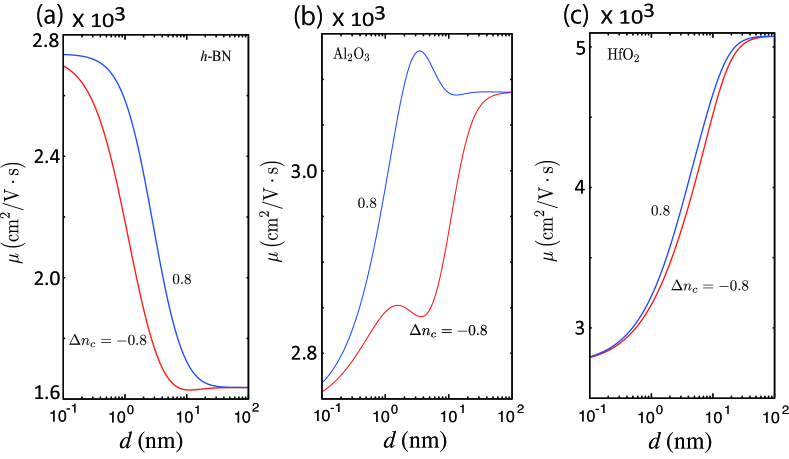
Figures 3(a)-(c) show the dependences of the total mobility at the interlayer distance for two different carrier polarizations and in the same dielectric environment as in Figs. 2(a)-(c), respectively. These mobilities are strongly affected by dielectric functions. In particular, when we choose as the middle dielectric, the mobility in Fig. 3(b) shows a dip for and a peak for , arising from the peak or dip structure in the dielectric functions, as shown in Fig. 2(b).
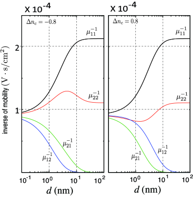
We show, in Fig. 4, the dependence of the four components of the inverse of the mobility at (left) and (right). By comparing the left and right panels in Fig. 4, we find that the interlayer components and are exchanged by changing the carrier polarization. The intralayer component is almost unaffected by the inversion of the carrier polarization, because the dependence is canceled out in the effective potential [Eq. (11)] for .
On the other hand, another intralayer component, , considerably depends on the interlayer distance and carrier density polarization. The reason for this is that the dependence of the dielectric function cannot be canceled out in the effective potential [Eq. (12)]. We found that the characteristic and dependences of the carrier mobility for were dominated by one of the intralayer components, i.e., .
In summary, we have investigated the carrier transport of GDLS in the presence of carrier polarization by extending our previous theory. We showed that the carrier mobility considerably depends on the carrier density polarization when the dielectric environment parameters and are satisfied under the condition . Our result reveals that the mobility can be improved by choosing higher-dielectric-constant materials as well as introducing the carrier polarization between two layers. From our results, we proposes guidelines for experiments on and applications of new functional atomically thin devices.
This work is supported by Grants-in-Aid for Scientific Research (KAKENHI) (Nos. 25107005, 25107001, 224710153, and 23310083) from the Japan Society for the Promotion of Science.
References
- [1] K. S. Novoselov and A. H. Castro Neto: Phys. Scr. T146 (2012) 014006.
- [2] S. Kim, I. Jo, J. Nah, Z. Yao, S. K. Banerjee, and E. Tutuc: Phys. Rev. B 83 (2011) 161401.
- [3] C. R. Dean, A. F. Young, I. Meric, C. Lee, L. Wang, S. Sorgenfre, K. Watanabe, T. Taniguchi, P. Kim, K. L. Shepard and J. Hon: Nat. Nanotechnol. 5 (2010) 722.
- [4] L. A. Ponomarenko, A. K. Geim, A. A. Zhukov, R. Jalil, S. V. Morozov, K. S. Novoselov, I. V. Grigorieva, E. H. Hill, V. V. Cheianov, V. I. Fal’ko, K. Watanabe, T. Taniguchi, and R. V. Gorbachev: Nat. Phys. 7 (2011) 958.
- [5] L. Britnell, R. M. Ribeiro, A. Eckmann, R. Jalil, B. D. Belle, A. Mishchenko, Y.-J. Kim, R. V. Gorbachev, T. Georgiou, S. V. Morozov, A. N. Grigorenko, A. K. Geim, C. Casiraghi, A. H. Castro Neto, and K. S. Novoselov: Science 340 (2013) 1311.
- [6] V. Ryzhii, T. Otsuji, M. Ryzhii, V. G. Leiman, S. O. Yurchenko, V. Mitin, and M. S. Shur: J. Appl. Phys. 112 (2012) 104507.
- [7] V. Ryzhii, A. A. Dubinov, T. Otsuji, V. Ya. Aleshkin, M. Ryzhii, and M. Shur: OPT EXPRESS 21 (2013) 25.
- [8] A. Ishikawa and T. Tanaka: Appl. Phys. Lett. 102 (2013) 253110.
- [9] A. A. Pikalov and D. V. Fil: Nanoscale Res. Lett. 7 (2012) 145.
- [10] M. P. Mink, H. T. C. Stoof, R. A. Duine, M. Polini, and G. Vignale: Phys. Rev. Lett. 108 (2012) 186402.
- [11] D. S. L. Abergel, M. Rodriguez-Vega, Enrico Rossi, and S. Das Sarma: Phys. Rev. B 88 (2013) 235402.
- [12] B. Scharf and A. Matos-Abiague: Phys. Rev. B 86 (2012) 115425.
- [13] T. Stauber and G. Gomez-Santos: Phys. Rev. B 85 (2012) 075410.
- [14] S. M. Badalyan and F. M. Peeters: Phys. Rev. B 85 (2012) 195444.
- [15] R. E. V. Profumo, R. Asgari, M. Polini, and A. H. MacDonald: Phys. Rev. B 85 (2012) 085443.
- [16] R. V. Gorbachev, A. K. Geim, M. I. Katsnelson, K. S. Novoselov, T. Tudorovskiy, I. V. Grigorieva, A. H. Macdonald, S. V. Morozov, K. Watanabe, T. Taniguchi, and L. A. Ponomarenko: Nat. Phys. 8 (2012) 896.
- [17] G. H. Lee, Y. J. Yu, C. Lee, C. Dean, K. L. Shepard, P. Kim, and J. Hone: Appl. Phys. Lett. 99 (2011) 2431144.
- [18] P. J. Zomer, S. P. Dash, N. Tombros, and B. J. van Wees: Appl. Phys. Lett. 99 (2011) 232104.
- [19] D. Jena and A. Konar: Phys. Rev. Lett. 98 (2007) 136805.
- [20] S. Adam, E. H. Hwang, V. M. Glitski, and. S. Das Sarma: Proc. Natl. Acad. Sci. U.S.A. 104 (2007) 1392.
- [21] C. Jang, S. Adam, J.-H. Chen, E. D. Williams, S. Das Sarma, and M. S. Fuhrer: Phys. Rev. Lett. 101 (2008) 146805.
- [22] S. Kim, J. Nah, I. Jo, D. Shahrjerdi, L. Colombo, Z. Yao, E. Tutuc, and S. K. Banerjee: Appl. Phys. Lett. 94 (2009) 062107.
- [23] B. Radisavljevic, M. B. Whitwick, and A. Kis: Nat. Nanotechnol. 6 (2011) 147.
- [24] M. J. Hollander, M. Labella, Z. R. Hughes, M. Zhu, K. A. Trumbull, R. Cavalero, D. W. Snyder, X. Wang, E. Hwang, S. Datta, and J. A. Robinson: Nano Lett. 11 (2011) 3601.
- [25] S.-L. Li, K. Wakabayashi, Y. Xu, S. Nakaharai, K. Komatsu, W.-W Li, Y.-F. Lin, A. Aparecido-Ferreira, and K. Tsukagoshi: Nano Lett 13 (2013) 3546.
- [26] K. Hosono and K. Wakabayashi: Appl. Phys. Lett. 103 (2013) 033102.
- [27] M. Kumagai and T. Takagahara: Phys. Rev. B 40 (1989) 12359.
- [28] T. Ando: J. Phys. Soc. Jpn. 75 (2006) 074716.
- [29] K. Nomura and A. H. MacDonald: Phys. Rev. Lett. 96 (2006) 256602.
- [30] B.G. Frederisk, G. Apai, and T. N. Rhodin: Phys. Rev. B 44 (1991) 1880.
- [31] S. Desgreniers and K. Lagarec: Phys. Rev. B59 (1991) 8467.
- [32] L. Kang, B. H. Lee, W.-J. Qi, Y. Jeon, R. Nieh, S. Gopalan, and J. C. Lee: IEEE Electron Device Lett. 21 (2000) 181.
- [33] T. Ando: J. Phys. Soc. Jpn. 75 (2006) 054701.