Josephson magnetic rotary valve
Abstract
We propose a control element for a Josephson spin valve. It is a complex Josephson device containing ferromagnetic (F) layer in the weak-link area consisting of two regions, representing and Josephson junctions, respectively. The valve’s state is defined by mutual orientations of the F-layer magnetization vector and normal to the interface separating and sections of the device. We consider possible implementation of the control element by introduction of a thin normal metal layer in a part of the device area. By means of theoretical simulations we study properties of the valve’s structure as well as its operation, revealing such advantages as simplicity of control, high characteristic frequency and good legibility of the basic states.
pacs:
74.45.+c, 74.50.+r, 74.78.Fk, 85.25.CpSuperconducting digital circuits based on Josephson junctions underwent significant progress in the last decades offering high frequency data receiving and processing (e.g. all-digital RF receiver with clock frequency of up to 30 GHz GKD ). Magnetic flux quantization in a superconducting loop, allowing representation of information bit as a flux quantum , is one of the key features providing the superconducting technology advantages. Unfortunately, a requirement to store the flux quantum in superconducting memory cells naturally limits possibilities of their miniaturization by geometric size of a cell providing the flux quantization inside it.
There is no such restriction in magnetic devices which rely on manipulation of local magnetizations. Their well known applications are random access memory and recording heads F . Recent advances in understanding of hybrid S-F structures involving the interplay of superconductivity (S) and ferromagnetism (F) opened exciting opportunities for developing the new tunable Josephson junction valves. Their operation relies on the control of induced superconducting correlations in the weak-link area by manipulations of magnetization of the F-layer located inside (or nearby) the Josephson heterostructure OYB1997 ; Beasley2006 ; BakurskiyAPL2013 or by changing the mutual orientations of magnetization vectors of multiple F-layers Blamire2004 ; BFE ; Robinson1 ; Kohlstedt ; Baek ; Halterman ; NDGWLPB , or by making use of the junction ground-state bistability GSWRKKK . Experimental realizations revealed the following drawbacks of these approaches.
1) Proper interplay between parts of spatially inhomogeneous bistable -junction, which separately possesses the phase shifted (0 and ) ground states, practically limits the junction dimension to the Josephson penetration length which is larger by an order of magnitude than the characteristic size of currently available junctions.
2) Modulation of the effective exchange energy by mutual misorientation of magnetization vectors , of the F films inside a SF1F2S structure requires combination of strong and weak ferromagnetics in order to provide the reversal of magnetization in just one film (with smaller coercivity) while keeping unchanged. In this case the magnetization reversal has little influence on magnitude of in the structure and the critical current of the valve is highly suppressed by . This in turn leads to decrease of the product of the spin valve down to few microvoltsBaek ( is the valve’s normal state resistance) that is to the value of three orders of magnitude smaller than that of junctions operating in rapid single flux quantum (RSFQ) circuits.
3) Suppression of the product in the SF1F2F3S valves based on spin-polarized triplet superconductivityBFE ; NDGWLPB is further enhanced (down to nanovolt level) due to an unavoidable decrease in caused by the increase in both: the number of non-superconducting layers and interfaces in the weak link region.
Small magnitude of limits utilization of SF1…FnS junctions as a control sFS unit of SIsFS devicesBakurskiyAPL2013 (I and s stand for an insulator and a thin superconducting layer) which have of millivolt scale that is typical for RSFQ circuits.
To resolve the problems we restrict ourselves by a single F-layer in the weak-link area and propose to create heterogeneity in the contact plane providing the separation of the structure into two regions which have positive (0 segment) and negative ( segment) critical current densities. If the size of the structure across the two segments ( axis in Fig. 1) is much less than then ground states of the Josephson phase in the segments become leveledBK ; GSWRKKK or (or if the critical currents of the segments are very close). Since this ground state is (or ) shifted from initial ground state of one (or both) of the segments, it corresponds to nearly unstable state of the structure BK ; GSWRKKK that manifests itself via significant reduction of the total structure critical current . We will show below that this leveling exists only when the F-layer magnetization vector is oriented in the - plane. However, if is aligned along the boundary between the segments (along axis), the Josephson phase gradient induced by the F-layer magnetic field shifts the values of in the segments closer to their initial values, thus removing the instability. Therefore misalignment of the F-layer magnetization from axis up to an angle of should lead to modulation of in a wide range.
Previously, the required inhomogeneity was experimentally realized by fabricating a step in the F layer thickness in the weak link region of SFS sandwiches SFSstep or SIFS tunnel junctions SIFSstep1 , SIFSstep4 . The devices were modeled theoretically SIFSstepT by considering the SIFS structures with a constant thickness of the F film and step-like variation of transparency of the SF interface. Both of these solutions provide a strong couplingSIFSstep4 between the 0, segments in the devices.
In this work we prove the validity of the above statement about wide-range modulation of by studying the example of a structure in which 0 and segments are formed by applying the normal film in the weak link area, as shown in Fig. 1. The existence of an NF interface inside the weak link region provides better decoupling of its 0 and segments, the property that is necessary to provide the effective operation of the device. At the same time, the presence of the N film is able to provide the required shift in the ground states of the segmentsHPKGKKRWK . We study modulation of the S-F/NF-S junction total critical current accompanied by changing of its current-phase relation. Finally, we briefly discuss the advantages of the proposed valve and a possible way of its utilization.
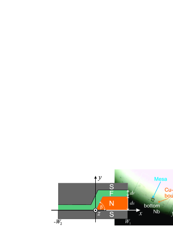
The considered multilayered S-F/NF-S structure consists of superconducting electrodes separated by either F-layer with a thickness or by the sandwich containing combination of the same F-layer and the N-layer having thickness . To describe a supercurrent transport we assumed that the effective electron-phonon coupling constant is zero and that the conditions of the dirty limit are fulfilled for both N and F metals. We also assumed that the superconducting films are made from the same material and that the temperature is close to the critical temperature that permits the using of the linearized Usadel equations: Usadel
| (1) | |||||
| (2) |
Here is the differential operator, , , are the Matsubara frequencies, is the exchange energy of the F material, are the decay lengths ( are the diffusion coefficients) in N, F metals, while are the Usadel Green’s functions in the N and F layers, respectively. Applying the Kupriyanov-Lukichev boundary conditions KL at all interfaces, we supposed that the suppression parameter at the SF interface is large enough to neglect suppression of superconductivity in the S electrodes. Here and are the resistance and the area of the SF interfaces, is the resistivity of F material. Contrary to this, the SN and the NF interfaces are supposed to be transparent for electrons. To simplify the problem further we suppose that the thickness of the N layer is small , the step in the F film is vertical suppl , and neglect the impact of the boundary region to the supercurrent. Under these suggestions the problem can be reduce to the one-dimensional, suppl resulting in the superconducting current densities in SFS () and SNFS () segments of the structure in the form:
| (3a) | |||
| (3b) | |||
| Here is the magnitude of order parameter in the S electrodes, are the lengths of the SFS and the SNFS regions shown in Fig. 1, is the electron charge. | |||
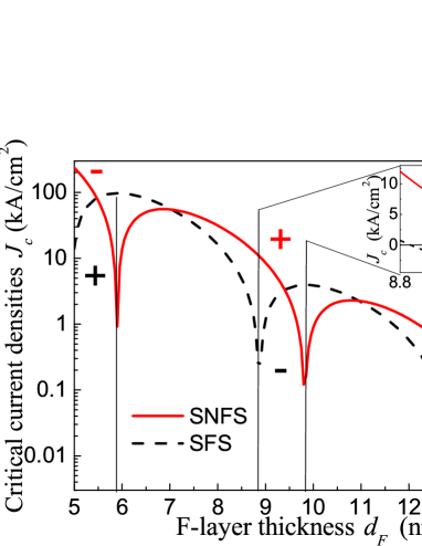
Figure 2 gives dependencies of SFS and SNFS segments of the structure. The calculations have been done for K and for a typical experimental set of parameters Bol , namely nm, K, , nm, nm. It is seen that the N-layer shifts the 0- transitions toward the larger values of the F-layer thickness. As a result, there are intervals of in which the critical current densities of the parts are of opposite sign. The distinction in curves demonstrated in Fig. 2 is not due to the finite thickness of the normal filmHPKGKKRWK but follows from the difference in the boundary conditions at the SF and NF interfaces.
Taking into account the step-like dependence suppl (3a), (3b) of the total critical current density versus coordinate we have used the two-dimensional sine-Gordon equation
| (4) |
for simulation of the structure total critical current modulation with rotation of the F-layer magnetization in the contact () plane. The space coordinates and are normalized to , the time is normalized to the inverse plasma frequency , is the damping coefficient, , , is the capacitance. The critical current density as well as the overlap bias current density is normalized to the critical current density of the SNFS segment . The ratio of critical current densities of the structure segments was taken in accordance with our theoretical estimations (for nm, see Fig. 2). Magnetization of the F-layer enters into consideration through the components , with the standard normalization: , where is the vacuum permeability and is the magnetic thickness of the structure. The structure was assumed to be square shaped with the side length and equal lengths of its 0, segments .
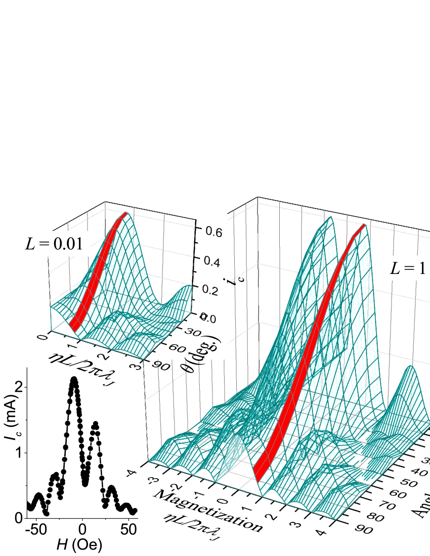
The total normalized critical current versus the magnetization for different angles of the magnetization’s deviation from the axis in the - plane is presented in Fig. 3. The dependence has minimum at zero magnetization for . At the same time, for magnetization oriented perpendicular to the boundary between the segments (along the axis, ) the dependence has Fraunhofer-like shape that is typical for 0- junctions PKKKGWFLU . It is seen that the critical current modulation with rotation of the magnetization is most pronounced for the magnetization values . To reveal the interplay between the structure 0- inhomogeneity and the F-layer magnetization value and its orientation we calculated harmonic amplitudes of the current-phase relation (CPR): .
Changing of the amplitudes and with the magnetization increase at zero angle is shown in Fig. 4a. The second harmonic in the CPR at appears due to spontaneous modulation of the current along the junction BK . In our case the amplitude of the harmonic is relatively small and insufficient for formation of a -junction (this requires BK ), and therefore the ground state is nondegenerated with . This corresponds to the noticeable difference of the critical current densities and the small dimension of the structure PKKKGWFLU . Increase of the magnetization induces an asymmetry of Josephson energy potential that manifests itself in occurrence of the cosine component in the CPR and according ground-state shift. The total critical current increase and the second harmonic decrease illustrate the mentioned compensation of spontaneous phase leveling by F-layer inner magnetic field. This effect is maximal in the vicinity of the magnetization value .
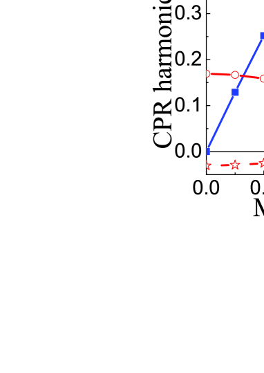
Modulation of the harmonic amplitudes with rotation of the magnetization for is presented in Fig. 4b. The critical current suppression (according curve is painted over in Fig. 3) corresponds to the reduction of the cosine component while the sine ones are kept nearly unchanged. This means that the modulation can be attributed to compensation of the Josephson phase leveling across the structure (along the axis) while the suppression due to existence of the inner magnetic field remains the same. The valve operation thus can be described in the frame of a simple single-harmonic model, like the conventional RSJ RSJ one, but taking into account the ground-phase shift (shown in the inset of Fig. 4b) and the critical current modulation, which in our case is of an order of magnitude.
We have fabricatedBol Nb-based S-F/NF-S junction using Cu as the N metal and Cu0.47Ni0.53 as the F film. Our process included formation of Copper rectangle on the bottom Nb followed by ion cleaning in argon plasma and in-situ CuNi-Nb bilayer deposition. Mesa was prepared to be splited by NF boundary (see Fig. 1). Thicknesses of the layers and material constants correspond to those used in the calculations. For this sample we had observed a minimum at zero magnetic field (see the bottom inset in Fig. 3), which is common for 0- junctions, while reference SFS- and SNFS-junctions have ideal Fraunhofer-shaped dependences of critical current versus applied magnetic field . However, CuNi appeared to be an inconvenient material to implement the valve due to its small scale domain structure, out-of-plane magnetic anisotropyVeshchunov and the absense of in-plane magnetization at relatively weak magnetic fields. More convenient ferromagnetic material is Pd0.99Fe0.01, possessing opposite to CuNi properties. It demonstratesBolginov sufficient magnetic hysteresis at low magnetic fields below Oe. Experimental study of S-F/NF-S contacts based on PdFe is an urgent task of our nearest research.
To reach the value typical for RSFQ circuits the considered structure can be used as a control element in SIsFS device BakurskiyAPL2013 ; BKSKG . Due to small thickness, the intermediate s-layer can not screen the F-layer magnetic field and therefore its rotation can control the whole SIs-F/NF-S junction critical current. At the same time, if the s-layer thickness is much larger than its coherence length so that then the characteristic frequency of the junction is determined by its SIs part and can reach the values typical for standard SIS junctions.
In conclusion, we have suggested magnetic Josephson valve based on interplay between spatial inhomogeneity of its structure and orientation of its F-layer magnetization. The valve can be easily operated by application of mutually orthogonal magnetic fields while its states are well distinguishable due to the large critical current modulation. The device possesses non-volatility, the ability of non-destructive read-out, and can be used in SIs-F/NF-S structure possessing high characteristic frequency. Since the considered critical current modulation does not degrade with reduction of the structure size (see upper inset of Fig. 3) the valve allows miniaturization. Decrease of the device dimensions in the direction normal to the boundary between its segments (along the axis) implies proportional increase of the F-layer magnetization and decrease of its thickness.
This work was supported by RFBR grants no. 13-02-01106, l4-02-90018-bela, 14-02-31002-mola, Ministry of Education and Science of the Russian Federation in the frameworks of grants no. 14.616.21.0011 and 14.587.21.0006 and Increase Competitiveness Program of NUST MISiS (K2-2014-025), Russian President grant MK-1841.2014.2, Dynasty Foundation, Scholarship of the President of the Russian Federation and Dutch FOM.
References
- (1) D. Gupta, D. E. Kirichenko, V. V. Dotsenko, R. Miller, S. Sarwana, A. Talalaevskii, J. Delmas, R. Webber, S. Govorkov, A. F. Kirichenko, I. V. Vernik, and Jia Tang IEEE Trans. Appl. Supercond. 21, 883 (2011).
- (2) A. Fert, Rev. Mod. Phys. 80, 1517 (2008).
- (3) S. Oh, D. Youm, and M. Beasley, Appl. Phys. Lett. 71, 2376 (1997).
- (4) R. Held, J. Xu, A. Schmehl, C. W. Schneider, J. Mannhart, and M. Beasley, Appl. Phys. Lett. 89, 163509 (2006).
- (5) S. V. Bakurskiy, N. V. Klenov, I. I. Soloviev, V. V. Bol’ginov, V. V. Ryazanov, I. I. Vernik, O. A. Mukhanov, M. Yu. Kupriyanov, and A. A. Golubov, Appl. Phys. Lett. 102, 192603 (2013).
- (6) C. Bell, G. Burnell, C.W. Leung, E. J. Tarte, D.-J. Kang, and M. G. Blamire, Appl. Phys. Lett. 84, 1153 (2004).
- (7) F. S. Bergeret, A. F. Volkov and K. B. Efetov, Rev. Mod. Phys. 77, 1321 (2005).
- (8) J. W. A. Robinson, J. D. S. Witt, and M. G. Blamire, Science 329, 59 (2010).
- (9) D. Sprungmann, K. Westerholt, H. Zabel, M. Weides, and H. Kohlstedt, Phys.Rev.B 82, 060505 (R) (2010).
- (10) B. Baek, W. H. Rippard, S. P. Benz, S. E. Russek, and P. D. Dresselhaus, Nat. Commun. 5, 3888 (2014).
- (11) M. Alidoust and K. Halterman, Phys. Rev. B 89, 195111 (2014).
- (12) B. M. Niedzielski, S. G. Diesch, E. C. Gingrich, Y. Wang, R. Loloee, W. P. Pratt, N. O. Birge, IEEE Trans. Appl. Supercond. 24,1800307 (2014).
- (13) E. Goldobin, H. Sickinger, M. Weides, N. Ruppelt, H. Kohlstedt, R. Kleiner, and D. Koelle, Appl. Phys. Lett. 102, 242602 (2013).
- (14) A. Buzdin, A. E. Koshelev, Phys. Rev. B 67, 220504(R) (2003).
- (15) S. M. Frolov, D. J. Van Harlingen, V. V. Bolginov, V. A. Oboznov, and V. V. Ryazanov, Phys. Rev. B 74, 020503(R) (2006).
- (16) M. Weides, C. Schindler, and H. Kohlstedt, J. Appl. Phys. 101, 063902 (2007).
- (17) M. Kemmler, M. Weides, M. Weiler, M. Opel, S. T. B. Goennenwein, A. S. Vasenko, A. A. Golubov, H. Kohlstedt, D. Koelle, R. Kleiner, and E. Goldobin, Phys. Rev. B 81, 054522 (2010).
- (18) N. Pugach, M. Kupriyanov, A. Vedyayev, C. Lacroix, E. Goldobin, D. Koelle, R. Kleiner, and A. Sidorenko, Phys. Rev. B 80, 134516 (2009).
- (19) V. V. Bol’ginov, A. N. Rossolenko, D. S. Baranov, in Proceedings of International Symposyum ”Nanophysics and nanoelectronics” I, 2014, edited by M. L. Timoshenko, V. V. Sheina (Nizhniy Novgorod, 2014), p. 19.
- (20) D. M. Heim, N. G. Pugach, M. Yu. Kupriyanov, E. Goldobin, D. Koelle, R. Kleiner, N. Ruppelt, M. Weides, H. Kohlstedt, arXiv:1310.0567 (2014).
- (21) K. D. Usadel, Phys. Rev. Lett. 25, 507 (1970).
- (22) M. Yu. Kuprianov and V. F. Lukichev, Zh. Eksp. Teor. Fiz. 94, 139 (1988) [Sov. Phys. JETP 67, 1163 (1988)].
- (23) see online supplementary material at [] for details of critical current dencity calculations.
- (24) J. Pfeiffer, M. Kemmler, D. Koelle, R. Kleiner, E. Goldobin, M. Weides, A. K. Feofanov, J. Lisenfeld, and A. V. Ustinov, Phys. Rev. B 77, 214506 (2008).
- (25) W. C. Stewart, Appl. Phys. Lett. 12, 277 (1968); K. K. Likharev, Rev. Mod. Phys. 51, 101 (1979).
- (26) M. Weides, M. Kemmler, U. Peralagu, H. Kohlstedt, C. Gurlich, E. Goldobin, J. Pfeiffer, D. Koelle, R. Kleiner, Supercond. Sci. Technol. 23, 095007 (2010).
- (27) I. S. Veshchunov, V. A. Oboznov, A. N. Rossolenko,A. S. Prokofiev, L. Ya. Vinnikov, A. Yu. Rusanov, D. V. Matveev, Pis’ma Zh. Eksp. Teor. Fiz. 88, 873 (2008) [JETP Lett. 88, 758 (2008)].
- (28) V. V. Bol’ginov, V. S. Stolyarov, D. S. Sobanin,A. L. Karpovich, V. V. Ryazanov, Pis’ma Zh. Eksp. Teor. Fiz. 95, 412 (2012) [JETP Lett. 95, 366 (2012)].
- (29) S. V. Bakurskiy, N. V. Klenov, I. I. Soloviev, M. Yu. Kupriyanov, and A. A. Golubov, Phys. Rev. B 88, 144519 (2013).