Light matter interaction in WS2 nanotube-graphene hybrid devices
Abstract
We study the light matter interaction in WS2 nanotube-graphene hybrid devices. Using scanning photocurrent microscopy we find that by engineering graphene electrodes for WS2 nanotubes we can improve the collection of photogenerated carriers. We observe inhomogeneous spatial photocurrent response with an external quantum efficiency of 1% at 0 V bias. We show that defects play an important role and can be utilized to enhance and tune photocarrier generation.
Heterostructure devices of transition metal dichalcogenides (TMDCs) and graphene have generated considerable research interest recently because of their superior optical and electronic properties.Britnell et al. (2013); Withers et al. (2014) The semiconducting nature of TMDCs combined with the presence of van Hove singularities in their electronic density of states allows for efficient photon absorption and carrier generation under optical excitation.Carvalho et al. (2013) Combining this feature with the high mobility of graphene has led to optoelectronic studies of heterostructure devices comprising graphene and single layer TMDCs.Britnell et al. (2013); Carvalho et al. (2013); Britnell et al. (2012); Roy et al. (2013); Ganatra and Zhang (2014); Sun and Chang (2014) These devices have exhibited good quantum efficiency for photocurrent generation in the visible range. However, the fabrication of such heterostructures requires multiple exfoliation and transfer steps. TMDC nanotubesTenne et al. (1992) represent another alternative for such applications; nanowires offer an additional advantage because they can enhance the absorption of light through the formation of optical cavitiesKim et al. (2014); Frey et al. (1998) and quasi 1D structures are known to enhance light matter interaction by virtue of an enhanced joint density of states (JDOS).Dresselhaus et al. (2002) Silicon and carbon nanotubes have been shown to be promising materials for solar-cell applications.Tian et al. (2007); Wei et al. (2007) Similarly, TMDC nanotubes could also allow for large scale integration of on-chip optoelectronic elements. In addition, the curvature of the nanotubes can be used to engineer spin and valley based optoelectronic control in dichalcogenide systems.Xu et al. (2014) Here, we investigate the photoresponse of WS2 nanotubes with field-effect transistor geometry and the enhanced photoresponse properties of hybrid devices of WS2 nanotubes with graphene electrodes. One of the motivations for using graphene electrodes for the nanotube is to modulate the density of carriers in the electrodes and modify the Schottky barrier;Shih et al. (2014) the other motivation is to observe the spatial homogeneity of the photoresponse. We investigate the efficiency of these devices for photoconversion and attempt to understand the role of defects in modifying optoelectronic properties.Allen et al. (2009)
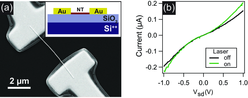
Prior to studying the hybrid devices, we probe individual WS2 nanotubes and show that they offer a good optoelectronic platform.Yang et al. (2008); Zhang et al. (2012a) We used WS2 multiwalled nanotubesTenne et al. (1992); Levi et al. (2013) obtained from NanoMaterials.apn Transmission electron microscope (TEM) images of the nanotubes (see Fig. S1 in supplementary material sup ) reveal that these are multi-walled hollow tubes of 50200 nm in diameter and have capped, or uncapped ends, where approximately half the diameter is hollow.Tenne et al. (1992) The nanotubes were drop coated on a 300 nm SiO2/Si chip for device fabrication. Standard electron-beam lithography techniques were used for device fabrication. Two probe devices were fabricated by sputtering Au to form metal contacts on the nanotubes as illustrated in Fig. 1(a). An in-situ Ar plasma cleaning system was used to remove resist residues under the electrodes before sputtering the metal without breaking the vacuum.
Fig. 1(b) shows the I-V characteristics of a WS2 nanotube device measured under ambient conditions. We find that the nanotube forms a Schottky-barrier contact, yielding non-linear current voltage characteristics because of band offsets of WS2 and gold.Kang et al. (2013) Although it has been reportedLevi et al. (2013) that similar devices exhibit n-type behavior, these nanotubes did not exhibit characteristic n or p-type behavior for a back gate voltage () of up to 50 V; this may be attributable to a different extent of doping compared with previous studies.Levi et al. (2013) In the presence of laser illumination, the device current increased because of photogenerated carriers in the nanotube. The measured photocurrent was observed to be as high as 30 nA in a device with an applied bias of 1 V.
To further understand the local nature of the photocurrent generation in our devices, we used scanning photocurrent microscopyLang and Henry (1978); Ahn et al. (2005); Balasubramanian et al. (2004); Gu et al. (2006) (see Fig. S3(a) in supplementary material sup for a schematic of the measurement setup). We applied a low frequency ( kHz) modulation to the laser using an acousto-optic modulator (AOM) and a lock-in technique to detect the photocurrent of the devices. From the response of the nanotube photocurrent to the frequency of modulation of the incident laser (see Fig. S4 in supplementary material sup ) we deduced a response time of ms for the WS2 nanotubes. This result is an improvement compared with the response times of other few/single layer devices of MoS2 and WS2 reported in the literatureYin et al. (2012); Perea-López et al. (2013); Choi et al. (2012) and is comparable to the projected value for WS2 nanotubes.Zhang et al. (2012a)
The reflected light, incident on the photodetector, was also measured using a lock-in amplifier, which provided information regarding the absorption of light by the material.Zhao et al. (2013); Jiang (2012) The map of the reflected light (see Fig. 4) indicates an absorption of 55 by the TMDC nanotube; similar values were obtained for WS2 thin filmsBallif et al. (1996) with an optical absorption coefficient cm-1 (see the supplementary material sup ).
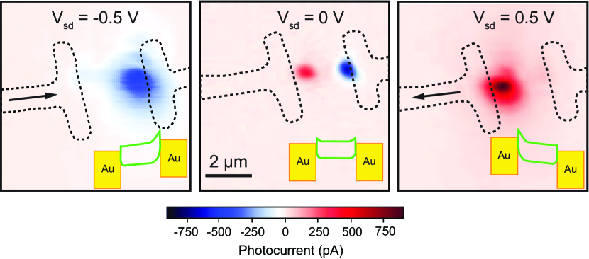
Fig. 2 presents the photocurrent map of a WS2 nanotube device. The electrode positions are outlined using an overlaid map of the reflected signal. We observe that the photocurrent is generated only near the nanotube-metal contact region where the Schottky barrier is present.Sun and Chang (2014); Fu et al. (2011); Kim et al. (2010); Ahn et al. (2005) The photocurrent decays into the nanotube away from the Schottky-barrier regions because of carrier diffusion in the nanotube. An exponential decay function was fitted to the photocurrent profile to extract information about the minority carrier diffusion length, , in the nanotube.Fu et al. (2011); Ubrig et al. (2014) The diffusion length was found to be 316 nm from the fit (see Fig. S4(a) in the supplementary material sup ). The diffusion length is related to the minority charge carrier lifetime, , and mobility, , by the relation , where is the Boltzmann constant, is the temperature and is the electronic charge. Using previously reported value of hole mobility Braga et al. (2012) in WS2, we find the carrier lifetime to be ns at room temperature. This result is comparable to the carrier lifetimes reported in the literature for other TMDC systems.Shi et al. (2013); Mouri et al. (2013); Choi et al. (2012)
The photoresponse as a function of the bias exhibits a shift in the photocurrent toward one of the electrodes with a change in the sign of the bias voltage. The applied bias voltage changes the Schottky-barrier heights of the electrodes asymmetrically, evoking a photoresponse from either end of the nanotube.Freitag et al. (2007a); Lee et al. (2007) Photocurrent maps were also generated as a function of the back gate voltage. However, similar to the electrical response, the photoresponse was also observed to be relatively insensitive to the gate voltage.
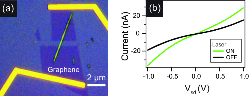
Combining the strong light matter interaction of the nanotubes with the superior electrical properties of graphene offers significant advantages in extraction of the generated photocarriers. Now we discuss the second device geometry involving WS2 nanotubes with graphene electrodes to study the effect on field effect and photocarrier collection. The fabrication of these devices involves electron beam lithography to fabricate a two probe device out of exfoliated graphene, followed by selective oxygen plasma etching to remove the middle portion of the graphene device leaving behind a slit. A dry transfer process is used to place a WS2 nanotube across the slit in the graphene (see Fig. S5 in supplementary material sup ). Experiments were conducted using different slit widths. An optical image of such a device is presented in Fig. 3(a). The I-V characteristic of the device presented in Fig. 3(b) demonstrate that the electrical behavior is similar to that of a two probe WS2 nanotube deviceZhang et al. (2012b) with metal contacts. We also fabricated similar hybrid devices using exfoliated MoS2 and WS2 nanotubes to explore photocarrier diffusionKang et al. (2013) at the TMDC junction. However, unlike the devices with WS2 nanotubes placed on graphene, the WS2 nanotube with MoS2 electrodes exhibited poor electrical contact.
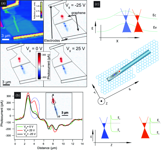
Although the field effect on the I-V characteristics remains weak, the quantum efficiency of the photoresponse of the graphene-WS2 hybrid devices is at zero bias voltage (see the supplementary material sup for details on quantum efficiency calculation). Fig. 4 shows the photoresponse of the graphene contacted WS2 nanotube device as a function of the gate voltage at 0 V bias voltage. We observe an inhomogeneous photoresponse along the length of the nanotube at zero bias voltage. At 0 V we see that photocurrent is generated near the interface between the graphene slit and the nanotubeWithers et al. (2014) as well as at the nanotube ends. This finding hints at the presence of band bending near the nanotube ends possibly due to the capped end (see Fig. S1 in supplementary materialsup for the TEM images).
As defects in the nanotube also modify the local electronic structure of the nanotube, we expect photocurrent generation where there is additional band bending. This phenomenon is observed in Fig. 4 as the appearance of an additional photocurrent spot with increasing gate voltage.Freitag et al. (2007b) These spots exhibit higher photoresponse than do other regions along the length of the nanotube. Several experiments have probed the consequences of such defects on the spatial variation of photoresponse of nanostructures.Fu et al. (2011); Allen et al. (2009); Lee et al. (2007); Freitag et al. (2007b, a); Balasubramanian et al. (2005) In these experiments, the effect of the defect is to create a local hill, or a valley, in the potential landscape. The photocarriers are generated in the same material that carries the charge carriers to the electrodes. This has the consequence that on either side of the local potential maxima and minima, the sign of the photocurrent changes as the local electric field changes.
In our experiments, the photocarriers generated in the WS2 nanotubes were extracted by the graphene electrodes. The interfacial electric field between a defect in the WS2 nanotube and the graphene results in the transfer of charge carriers. Because of the variation of the interfacial electric field across the span of the defect, the photocurrent also exhibits a local peak. There was no change in the sign of the photocurrent in our experiments because the sign of the interfacial electric field between the WS2 and the graphene did not change; however, its magnitude did change, reflecting a change in the photocurrent. Similar spots of large photoresponse were also seen in the work of Britnell et al.Britnell et al. (2013) Although the microscopic nature of the inhomogeneous photocurrent was not discussed in this reference, we believe that the origin was similar in an analogous device structure.
One possible mechanism that could modify the photoresponse is the modification of the workfunction of graphene,Yu et al. (2009) as this would result in a change in the interfacial electric field. However, not all spots in the spatial photoresponse map are modified as a function of gate voltage. The absence of a uniform modulation of the photoresponse suggests a more localized source away from the graphene.
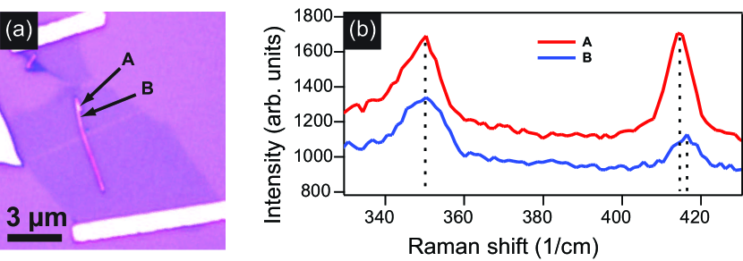
A recent studyNan et al. (2014) reported enhanced photoluminescence in cracked regions of MoS2 monolayers caused by the adsorption of oxygen in the sulfur vacancy regions accompanied by blue-shift of the mode in the Raman spectrum. Similarly, we observed a blue-shift of cm-1 in the peak of the nanotube at the defect site of the device (Fig. 5). The formation of these defect regions could be attributable to the ultrasonication of the nanotube solution or to the transfer process and also supports the role of the defects in the enhanced photoresponse observed in our graphene-WS2 devices. However, the resolution of our technique remains limited by the spot size of the incident laser and does not provide any direct insight regarding the microscopic nature of the defects. The presence of localized defects in carbon nanotubesFreitag et al. (2007b); Balasubramanian et al. (2005); Bockrath et al. (2001) has been studied extensively in the past, and similar defects are likely to exist in inorganic TMDC nanotubes. Our measurement provides a method of imaging defects in similar TMDC semiconductor systems.
In summary we fabricated hybrid devices using WS2 nanotubes and graphene that show good light matter interaction. We observed spatially inhomogeneous photoresponse in the nanotube and demonstrated a method of detecting defects in WS2 nanotubes using graphene contacts and scanning photocurrent microscopy. In addition to detecting defects we also observed a good external quantum efficiency () and enhanced photocarrier collection at zero bias voltage in these hybrid devices. The fabrication is simple and does not involve any post-processing because of the robustness of both graphene and WS2 nanotubes. The technique also allows for integration, as WS2 nanotubes can be synthesized in large quantities. The strong light matter interaction in dichalcogenide systems and ability of nanowire based structures to concentrate light offer opportunities for fabricating improved photoactive devices using dichalcogenide nanotubes.
We acknowledge fruitful discussion with Aniruddha Konar, IBM. This work was supported by the Swarnajayanti Fellowship from the Department of Science and Technology and, the Department of Atomic Energy of the Government of India.
References
- Britnell et al. (2013) L. Britnell, R. Ribeiro, A. Eckmann, R. Jalil, B. Belle, A. Mishchenko, Y.-J. Kim, R. Gorbachev, T. Georgiou, S. Morozov, A. N. Grigorenko, A. K. Geim, C. Casiraghi, A. H. Castro Neto, and K. S. Novoselov, Science 340, 1311 (2013).
- Withers et al. (2014) F. Withers, H. Yang, L. Britnell, A. P. Rooney, E. Lewis, A. Felten, C. R. Woods, V. Sanchez Romaguera, T. Georgiou, A. Eckmann, Y. J. Kim, S. G. Yeates, S. J. Haigh, A. K. Geim, K. S. Novoselov, and C. Casiraghi, Nano Letters 14, 3987 (2014).
- Carvalho et al. (2013) A. Carvalho, R. M. Ribeiro, and A. H. Castro Neto, Physical Review B 88, 115205 (2013).
- Britnell et al. (2012) L. Britnell, R. V. Gorbachev, R. Jalil, B. D. Belle, F. Schedin, A. Mishchenko, T. Georgiou, M. I. Katsnelson, L. Eaves, S. V. Morozov, N. M. R. Peres, J. Leist, A. K. Geim, K. S. Novoselov, and L. A. Ponomarenko, Science 335, 947 (2012).
- Roy et al. (2013) K. Roy, M. Padmanabhan, S. Goswami, T. P. Sai, G. Ramalingam, S. Raghavan, and A. Ghosh, Nature Nanotechnology 8, 826 (2013).
- Ganatra and Zhang (2014) R. Ganatra and Q. Zhang, ACS Nano 8, 4074 (2014).
- Sun and Chang (2014) Z. Sun and H. Chang, ACS Nano 8, 4133 (2014).
- Tenne et al. (1992) R. Tenne, L. Margulis, M. Genut, and G. Hodes, Nature 360, 444 (1992).
- Kim et al. (2014) S.-K. Kim, K.-D. Song, T. J. Kempa, R. W. Day, C. M. Lieber, and H.-G. Park, ACS Nano 8, 3707 (2014).
- Frey et al. (1998) G. Frey, R. Tenne, M. Matthews, M. Dresselhaus, and G. Dresselhaus, Journal of Materials Research 13, 2412 (1998).
- Dresselhaus et al. (2002) M. S. Dresselhaus, G. Dresselhaus, A. Jorio, A. G. Souza Filho, M. A. Pimenta, and R. Saito, Accounts of Chemical Research 35, 1070 (2002).
- Tian et al. (2007) B. Tian, X. Zheng, T. J. Kempa, Y. Fang, N. Yu, G. Yu, J. Huang, and C. M. Lieber, Nature 449, 885 (2007).
- Wei et al. (2007) J. Wei, Y. Jia, Q. Shu, Z. Gu, K. Wang, D. Zhuang, G. Zhang, Z. Wang, J. Luo, A. Cao, and D. Wu, Nano Letters 7, 2317 (2007).
- Xu et al. (2014) X. Xu, W. Yao, D. Xiao, and T. F. Heinz, Nature Physics 10, 343 (2014).
- Shih et al. (2014) C.-J. Shih, Q. H. Wang, Y. Son, Z. Jin, D. Blankschtein, and M. S. Strano, ACS Nano 8, 5790 (2014).
- Allen et al. (2009) J. E. Allen, D. E. Perea, E. R. Hemesath, and L. J. Lauhon, Advanced Materials 21, 3067 (2009).
- Yang et al. (2008) Y. Yang, H. E. Unalan, P. Hiralal, K. Chremmou, A. The, I. Alexandrou, R. Tenne, and G. Amaratunga, in Nanotechnology, 2008. NANO’08. 8th IEEE Conference on (IEEE, 2008) pp. 85–87.
- Zhang et al. (2012a) C. Zhang, S. Wang, L. Yang, Y. Liu, T. Xu, Z. Ning, A. Zak, Z. Zhang, R. Tenne, and Q. Chen, Applied Physics Letters 100, 243101 (2012a).
- Levi et al. (2013) R. Levi, O. Bitton, G. Leitus, R. Tenne, and E. Joselevich, Nano Letters 13, 3736 (2013).
- (20) NanoMaterials Ltd., Yavne, Israel.
- (21) See supplementary material at http://dx.doi.org/10.1063/1.4902983 for TEM images, measurement scheme, and data from another device.
- Kang et al. (2013) J. Kang, S. Tongay, J. Zhou, J. Li, and J. Wu, Applied Physics Letters 102, 012111 (2013).
- Lang and Henry (1978) D. V. Lang and C. H. Henry, Solid-State Electronics 21, 1519 (1978).
- Ahn et al. (2005) Y. Ahn, J. Dunning, and J. Park, Nano Letters 5, 1367 (2005).
- Balasubramanian et al. (2004) K. Balasubramanian, Y. Fan, M. Burghard, K. Kern, M. Friedrich, U. Wannek, and A. Mews, Applied Physics Letters 84, 2400 (2004).
- Gu et al. (2006) Y. Gu, J. P. Romankiewicz, J. K. David, J. L. Lensch, and L. J. Lauhon, Nano Letters 6, 948 (2006).
- Yin et al. (2012) Z. Yin, H. Li, H. Li, L. Jiang, Y. Shi, Y. Sun, G. Lu, Q. Zhang, X. Chen, and H. Zhang, ACS Nano 6, 74 (2012).
- Perea-López et al. (2013) N. Perea-López, A. L. Elías, A. Berkdemir, A. Castro-Beltran, H. R. Gutiérrez, S. Feng, R. Lv, T. Hayashi, F. López-Urías, S. Ghosh, B. Muchharla, and M. Terrones, Advanced Functional Materials 23, 5511 (2013).
- Choi et al. (2012) W. Choi, M. Y. Cho, A. Konar, J. H. Lee, G.-B. Cha, S. C. Hong, S. Kim, J. Kim, D. Jena, J. Joo, and S. Kim, Advanced Materials 24, 5832 (2012).
- Zhao et al. (2013) W. Zhao, Z. Ghorannevis, L. Chu, M. Toh, C. Kloc, P.-H. Tan, and G. Eda, ACS Nano 7, 791 (2013).
- Jiang (2012) H. Jiang, The Journal of Physical Chemistry C 116, 7664 (2012).
- Ballif et al. (1996) C. Ballif, M. Regula, P. Schmid, M. Remškar, R. Sanjines, and F. Lévy, Applied Physics A 62, 543 (1996).
- Fu et al. (2011) D. Fu, J. Zou, K. Wang, R. Zhang, D. Yu, and J. Wu, Nano Letters 11, 3809 (2011).
- Kim et al. (2010) C.-J. Kim, H.-S. Lee, Y.-J. Cho, K. Kang, and M.-H. Jo, Nano Letters 10, 2043 (2010).
- Ubrig et al. (2014) N. Ubrig, S. Jo, H. Berger, A. F. Morpurgo, and A. B. Kuzmenko, Applied Physics Letters 104, 171112 (2014).
- Braga et al. (2012) D. Braga, I. Gutie rrez Lezama, H. Berger, and A. F. Morpurgo, Nano Letters 12, 5218 (2012).
- Shi et al. (2013) H. Shi, R. Yan, S. Bertolazzi, J. Brivio, B. Gao, A. Kis, D. Jena, H. G. Xing, and L. Huang, ACS Nano 7, 1072 (2013).
- Mouri et al. (2013) S. Mouri, Y. Miyauchi, and K. Matsuda, Nano Letters 13, 5944 (2013).
- Freitag et al. (2007a) M. Freitag, J. C. Tsang, A. Bol, D. Yuan, J. Liu, and P. Avouris, Nano Letters 7, 2037 (2007a).
- Lee et al. (2007) E. J. Lee, K. Balasubramanian, J. Dorfmüller, R. Vogelgesang, N. Fu, A. Mews, M. Burghard, and K. Kern, Small 3, 2038 (2007).
- Zhang et al. (2012b) C. Zhang, Z. Ning, Y. Liu, T. Xu, Y. Guo, A. Zak, Z. Zhang, S. Wang, R. Tenne, and Q. Chen, Applied Physics Letters 101, 113112 (2012b).
- Freitag et al. (2007b) M. Freitag, J. C. Tsang, A. Bol, P. Avouris, D. Yuan, and J. Liu, Applied Physics Letters 91, 031101 (2007b).
- Balasubramanian et al. (2005) K. Balasubramanian, M. Burghard, K. Kern, M. Scolari, and A. Mews, Nano Letters 5, 507 (2005).
- Yu et al. (2009) Y.-J. Yu, Y. Zhao, S. Ryu, L. E. Brus, K. S. Kim, and P. Kim, Nano Letters 9, 3430 (2009).
- Nan et al. (2014) H. Nan, Z. Wang, W. Wang, Z. Liang, Y. Lu, Q. Chen, D. He, P. Tan, F. Miao, X. Wang, J. Wang, and Z. Ni, ACS Nano 8, 5738 (2014).
- Bockrath et al. (2001) M. Bockrath, W. Liang, D. Bozovic, J. H. Hafner, C. M. Lieber, M. Tinkham, and H. Park, Science 291, 283 (2001).