Dispersion Corrected DFT Study of Pentacene Thin Films on Flat and Vicinal Au(111) Surfaces
Abstract
Here we a present a density functional theory study of pentacene ultra-thin films on flat [(111)] and vicinal [(455)] Au surfaces. We have performed crystal and electronic structure calculations by using PBE and optB86b-vdW functionals and investigated the effects of long range Van der Waals interactions for different coverages starting from a single isolated molecule up to 4 monolayers of coverage. For an isolated molecule both functionals yield the hollow site as the most stable one with bridge-60 site being very close in energy in case of optB86b-vdW. Binding strength of an isolated pentacene on the step edge was found to be much larger than that on the terrace sites. Different experimentally reported monolayer structures were compared and the (6 3) unit cell was found to be energetically more stable than the () and () ones. For one monolayer films while dispersion corrected calculations favored flat pentacene molecules on terraces, standard (PBE) calculations either found tilted and flat configurations to be energetically similar (on (111) surface) or favored the tilted configuration (on (455) surface). PDOS calculations performed with optB86b-vdW functional showed larger dispersion of molecular orbitals over the Au states for the (455) surface when compared with the (111) surface, indicating an enhanced charge carrier transport at the pentacene-gold interface in favor of the vicinal surface. Starting with the second monolayer, both functionals favored tilted configurations for both surfaces. Our results underline the importance of the dispersion corrections for the loosely bound systems like pentacene on gold and the role played by step edges in determining the multilayer film structure and charge transfer at the organic molecule-metal interface.
keywords:
vdW-DF Calculations, Pentacene, Au Surfaces, Step Edges1 Introduction
In the last 30 years organic electronics have evolved to a point that commercial devices are now a part of our lives in the form of, for example, organic light emitting diodes and lightening applications. Nevertheless, there are still many issues that need a fundamental understanding and further development.1, 2, 3, 4 Pentacene is one of the most studied small molecule organic semiconductors and find use in field effect transistors.3, 5, 6 Among the many factors that affect the performance of an OFET are the charge transfer at the metal electrode/organic semiconductor interface and the mobility of the charges in organic semiconductor film.1, 2, 3, 4, 5, 6 Both of these factors are in turn, directly or indirectly, correlated to the structure and morphology of the organic film on the metal electrode to a certain extent. Hence electronic and structural properties of pentacene films on metal surfaces have been investigated intensively both experimentally7, 8, 9, 10, 11, 12, 13, 14, 15, 16, 17, 18, 19 and theoretically.20, 21, 22, 23, 24, 25, 26, 27, 28, 29, 30, 31, 32, 33, 34, 35
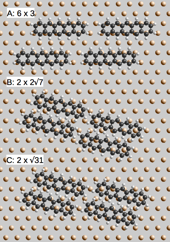
Since gold is the choice of electrode material in many devices, pentacene on Au surfaces have attracted particular interest.9, 11, 12, 13, 14, 15, 16, 21, 23, 24, 28, 35 By means of scanning tunneling microscopy (STM)10, 11, 14, 15, 16 and x-ray absorption spectroscopy (NEXAFS)16 several groups have reported similar full coverage monolayer structures with pentacene molecules lying flat on the Au (111) surface if not with a small tilt angle (NEXAFS results indicate an average tilt angle of 13∘ 16). These structures which will be referred to as “B” and “C” are shown in Fig. 1 and have packing density of about 1.1 x 10¹⁴ molecules/cm2. Recently we have performed a helium diffraction study of the Pen/Au(111)9 system and observed a commensurate 6 3 monolayer structure which we had also observed on Ag(111) surfaces7, 8 This monolayer phase which has a slightly lower packing density of 0.8 1014 molecules/cm2 is also shown in Fig. 1 and will be referred to as “A”. At higher coverages (starting with 2nd ML) Pen molecules still had their long axis parallel to surface but with a higher tilt angle resulting in multilayers structures similar to b-c face of the bulk Pen crystal.
Recently several density functional theory (DFT) studies of Pen/Au(111) have been performed focusing mostly on the electronic properties such as work function change of the Au surface upon pentacene adsorption.21, 22, 23, 24 In these studies either isolated pen molecules or one monolayer films were considered on Au(111) surface21, 22, 23 or on Au clusters24, without a systematic search for the best adsorption site/geometry and/or the crystal structure. Instead the electronic calculations were performed by using a chosen pentacene unit cell which were different then the experimentally determined ones described above. Nevertheless the calculated work function changes were in good agreement with the experimental value (0.95 eV 36) regardless of the functionals, methods or the unit cells used when the calculations were made on the Au(111) surfaces. In the cluster calculations of Dahnovsky et al.24, however, who studied the potential energy surface of pentacene and found a very a smooth landscape, the calculated work function change was much lower than the experimental value. Long range van der Waals interactions were considered in three of these studies with different approaches. Morikawa et al.23 employed DFT-D37 and vdW-DF38methods and found that while the former method well reproduces the Pen-substrate distance, the latter method well reproduces the binding energies. Dahnovsky et al. on the other hand employed CAM-B3LYP39, wB97 and wB97X40 long range correlated functionals and found the latter two functionals to reproduce the experimental binding energies accurately. Finally, Ortega et al.21 who employed LCAO-S2-vdW41 formalism for geometry optimization could achieve electronic structure results comparable to the experimental values.
Here we have systematically studied structural and electronic properties of pentacene on flat and vicinal Au(111) surface as a function of coverage by means of van der Walls density functional theory (vdW-DF) calculations. We first studied isolated molecules to determine the most preferred adsorption site and the potential energy surface. Then we have examined different monolayer structures which were reported in the literature. Finally we have investigated higher coverage films up to four monolayers. By this way we were able to monitor the evolution of the electronic and structural properties of the pen films as a function of film thickness and unit cell structure.
2 Theoretical Methods
In order to describe the morphology and the electronic structures of Pen multilayers on flat and vicinal Au(111) surfaces, we performed van der Waals (vdW) density functional theory (DFT) calculations based on projector augmented waves (PAW)42 method available in VASP.43, 44, 45 A self-consistent implementation of the vdW-DF method of Dion et al.38 was used as a non-local correlation functional which accounts for the dispersion interactions. The exchange part was treated with optB86b functional which is optimized for the correlation part. For the prediction of material properties, the optB86b-vdW approach has been recently shown to improve over standard and revised exchange-correlation (XC) schemes like PBE, revPBE and PBEsol.45
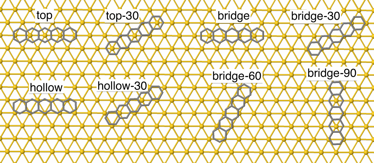
Four layer slab models were constructed from the bulk phase of gold to represent the flat and vicinal Au(111) surfaces. The ionic positions were optimized by minimizing the Hellmann-Feynman forces until a threshold value of 0.01 eV/Å was reached on each atom. After a full relaxation of the slab geometries, the displacement of the atoms from their bulk positions remained to be less than Å. Therefore the slab thickness is found to be sufficient to represent Au(111) surface properties. Then, in order to speed up the calculations we only kept the Au atoms at the bottom layer of the slabs frozen to their bulk positions. Isolated Pen molecules were considered on the 58 flat slab to accommodate sufficiently large separation between their periodic images. All possible adsorption configurations were taken into account as shown in Fig. 2. Single and multi layer Pen coverages were modeled on the flat Au(111)-36 supercell. We considered different Pen monolayer phases as seen in Fig.1 Several probable adsorption configurations were built for the Pen mono- and multilayers similar to the isolated case. For the vicinal Au(111) surface, an Au(455) supercell was built with a terrace size of 19.8 Å along [11]. A vacuum space with a height of least 13 Å was introduced to prevent any unphysical interaction between the periodic images of the slabs. All calculations were performed both at the standard DFT level with PBE XC functional and at the vdW-DF level with optB86b-vdW approach.
The interactons between the ionic cores and the valence electrons have been treated within the PAW method using plane waves up to a cutoff energy of 370 eV. Brillouin zone sampling was performed on a -point mesh of 441. The density of states (DOS) calculations have been carried out with doubly denser -point meshes. These parameters were tested and optimized to get well converged total energies of the physical structures considered in this work.
We estimated the binding energies of Pen molecules on Au(111) surface by,
where , and are the total energies of the Pn/Au(111) combined system, of the bare Au(111) slab and of a single Pn in a big box, respectively.
3 Results and Discussion
Gold forms in a ccp crystal structure having a space group symmetry of Fmm (225) with a bulk lattice constant of 4.078 Å.47 Standard PBE overestimates it leading to a value of 4.160 Å due to the inherent tendency of the LDA to distribute charge uniformly which is not the case especially in metals. The vdW-DF method better predicts the lattice constant to be 4.125 Å through the formulation of the long ranged dispersive effects the correlation part and the optimization of exchange energy, so called the optB86b functional.
| Site | PBE | optB86b-vdW | ||
|---|---|---|---|---|
| Et (eV) | (Å) | Et (eV) | (Å) | |
| top | 0.025 | 4.06 | 0.033 | 3.25 |
| top-30 | 0.035 | 4.07 | 0.201 | 3.08 |
| bridge | 0.211 | 4.09 | 0.243 | 3.14 |
| bridge-30 | 0.213 | 4.08 | 0.176 | 2.96 |
| bridge-60 | 0.190 | 4.07 | 0.007 | 2.94 |
| bridge-90 | 0.206 | 4.09 | 0.106 | 3.10 |
| hollow | 0.000 | 3.87 | 0.000 | 2.94 |
| hollow-30 | 0.029 | 4.00 | 0.145 | 3.12 |
Isolated Pentacene on Au(111). The possible adsorption sites and orientations of a single pentacene on the flat Au(111) surface are presented in Figure 2. A Pen molecule can be considered as isolated on a sufficiently large (8 5) Au surface cell on which the separation between its periodic images is at least 8 Å. Each of the possible initial geometries were relaxed including additional standing-up configurations which are energetically 0.5 eV (vdW included) less favorable relative to the planar cases. Both the standard and vdW DFT calculations find the hollow configuration as the minimum energy adsorption site as seen in Table. 1. The relative total energies between different adsorption orientations get as large as 0.2 eV per molecule suggesting a rather shallow plateau-like potential energy surface (PES) for the flat Au(111) termination. France et al. determined the adsorption energy as 110 kJ/mol from initial monolayer of Pen on the Au(111) surface by performing temperature-programmed desorption (TPD) experiments.11 The standard PBE significantly underestimates the binding energy of a single Pen on the flat Au surface. Its prediction is a weak adsorption at the hollow site with an energy of 0.332 eV (32 kJ/mol) at a height of 3.87 Å. Moreover, the penalty in the energy from the planar to a slightly tilted position is negligibly small with the PBE functional. However, the relaxation with the vdW-DF method gives a binding energy of 1.337 eV (129 kJ/mol) per molecule preferring the planar adsorption at a relatively shorter height of 2.94 Å at the hollow site. Our vdW-DF calculations reveal that the bridge-60 and the hollow configurations are energetically similar. Pen molecules at the both adsorption orientations follow the lattice symmetry similarly. This indicates that the matching between the molecular and surface charge densities is an important factor in the determination of the preferential adsorption site. In fact in our previous DFT calculations for Pen on Ag(111), bridge 60 and hollow configurations were also found to be very close in energy, bridge 60 being slightly more stable (by 8 meV).26
The small energy differences between different adsorption orientations in Table 1 indicate a rather flat potential energy surface (PES) which could allow the diffusion of the Pen molecules at the contact layer. For instance, physisorbed Pen molecules were reported to be dragged by the STM tip during image acquisition on the Au(111) surface.48
| Film | Site | Et | ||||||||
|---|---|---|---|---|---|---|---|---|---|---|
| 1 ML | top | 0.022 | 3.98 | 0.0(0.5) | ||||||
| bridge-60 | 0.000 | 3.98 | 0.0(0.8) | |||||||
| hollow | 0.003 | 3.99 | 0.0(0.5) | |||||||
| 2 ML | flat@bridge-60 | 0.061 | 3.94 | 3.64 | 0.0(1.4) | 0.0(1.3) | ||||
| top | 0.062 | 3.91 | 3.51 | 0.0(3.0) | 21.7(4.7) | |||||
| bridge-60 | 0.032 | 3.67 | 3.67 | -3.5(2.8) | 20.5(5.0) | |||||
| hollow | 0.000 | 3.67 | 3.65 | -10.3(2.9) | 20.3(5.0) | |||||
| 3ML | top | 0.002 | 3.81 | 3.81 | 3.81 | -7.5(5.8) | 24.4(4.7) | -24.9(3.4) | ||
| bridge-60 | 0.000 | 3.81 | 3.46 | 3.71 | -5.4(1.7) | 25.1(6.3) | -22.9(3.2) | |||
| hollow | 0.032 | 3.81 | 3.46 | 3.54 | -7.6(3.8) | 22.2(5.6) | -25.1(3.9) | |||
| 4ML | top | 0.001 | 3.78 | 3.11 | 3.46 | 3.81 | -10.3(8.5) | 25.2(9.6) | -26.5(5.1) | 28.2(4.5) |
| bridge-60 | 0.000 | 3.42 | 3.52 | 3.63 | 3.64 | -6.2(4.1) | 25.4(5.6) | -24.7(3.7) | 21.6(3.7) | |
| hollow | 0.087 | 3.46 | 3.17 | 3.41 | 3.81 | -4.9(3.7) | 21.5(8.9) | -26.1(4.6) | 22.2(3.3) |
| Film | Site | Et | ||||||||
|---|---|---|---|---|---|---|---|---|---|---|
| 1 ML | top | 0.183 | 3.25 | 0.0 | ||||||
| bridge-60 | 0.000 | 3.12 | 0.0 | |||||||
| hollow | 0.008 | 3.13 | 0.0 | |||||||
| 2 ML | flat@bridge-60 | 0.070 | 3.13 | 3.11 | 0.0(0.0) | 0.0(0.0) | ||||
| top | 0.116 | 3.13 | 2.95 | 0.0(6.3) | 13.7(4.7) | |||||
| bridge-60 | 0.000 | 3.11 | 2.90 | 0.0(2.0) | 12.4(4.7) | |||||
| hollow | 0.014 | 3.12 | 2.93 | 0.0(2.0) | 12.2(5.3) | |||||
| 3ML | top | 0.108 | 3.12 | 3.07 | 3.12 | 0.0(7.5) | 10.0(2.9) | -9.9(-2.0) | ||
| bridge-60 | 0.003 | 3.11 | 3.07 | 3.12 | 0.0(2.0) | 10.4(2.3) | -9.5 (-1.3) | |||
| hollow | 0.000 | 3.09 | 3.05 | 3.12 | 0.0(2.1) | 13.1(3.0) | -12.0(-1.5) | |||
| 4ML | bridge-60 | 0.016 | 3.10 | 3.11 | 3.12 | 3.12 | 0.0(1.9) | 13.9(2.0) | -13.4(-2.4) | 10.1(-1.4) |
| hollow | 0.000 | 3.09 | 3.10 | 3.10 | 3.12 | 0.0(1.9) | 13.7(0.6) | -12.4(-4.5) | 11.1(-2.4) |
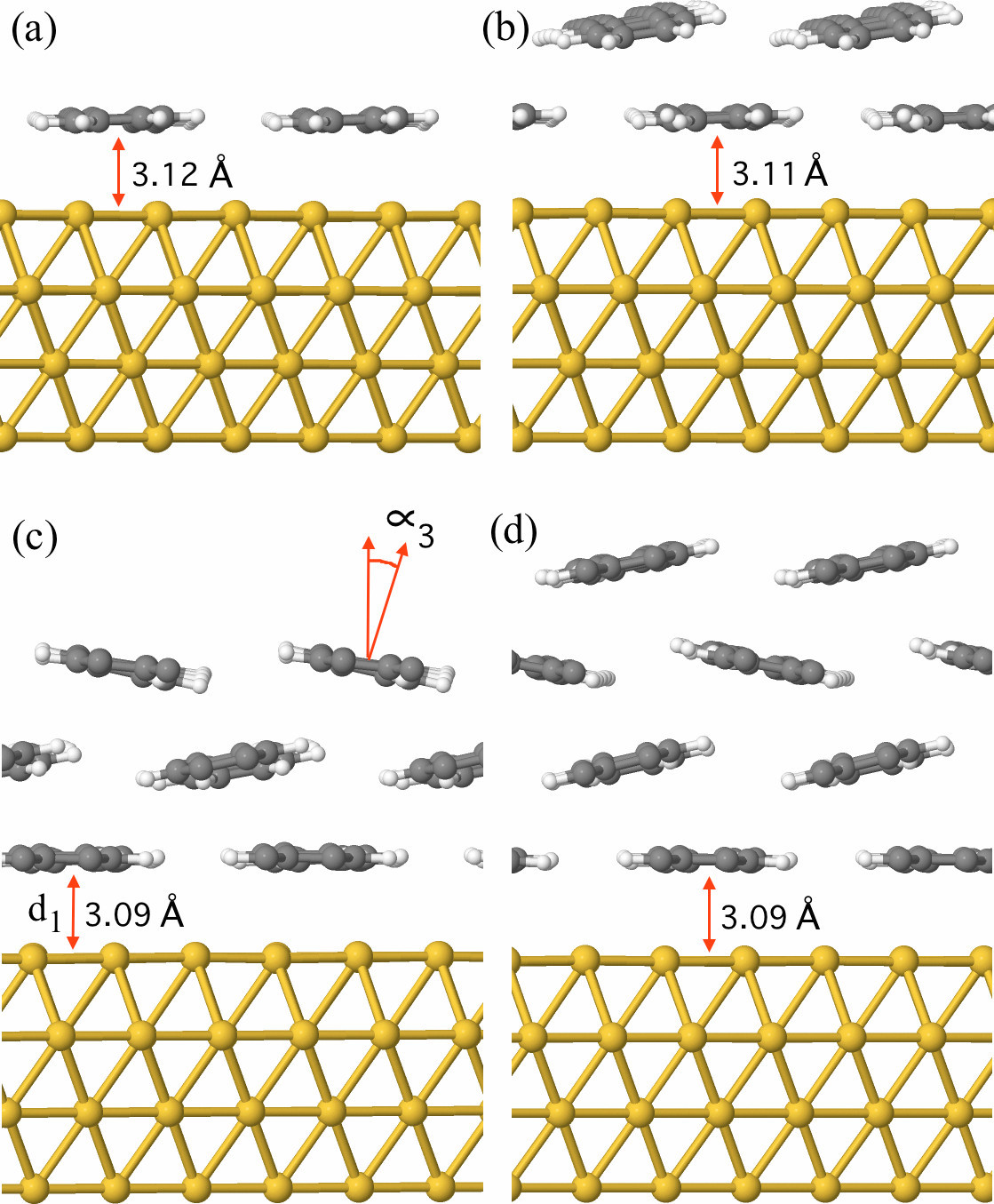
Monolayer on Flat Au(111). A full Pen monolayer coverage has been modeled on an experimentally observed 639 Au(111) surface unit cell, referred as the phase A in Figure 1. We considered a number of probable configurations including top, bridge-60, and hollow sites for the molecules on this contact layer. We optimized the initial geometries by using both the standard PBE and the optB86b-vdW methods. The minimum energy adsorption leads to the bridge-60 position which is only slightly preferable over the hollow site as presented in Table 2 and Table 3. The computational cell structure of the phase A is not commensurate with those of the phases B and C as seen in Figure 1. To compare their energetics and interpret these results for the relative stabilities, we calculated the binding energies of the full monolayer in each case. The corresponding values are obtained as 0.23 eV, 0.17 eV , and 0.15 eV for the phases A, B and C, respectively. Hence, the adsorption of the contact layer is energetically more preferable with the 63 cell structure on the Au(111) surface. Nevertheless, all these three configurations are very close in energy which explains why pentacene has so many different monolayer phases/structures that form simultaneously on the Au(111) surface. Due to in-plane intermolecular interactions, the binding energy in the full monolayer coverage substantially drops relative to the single isolated adsorption case. The standard PBE calculations predict much weaker Pen-Au interaction compared with the vdW-DF results. For instance, the adsorption height of the full monolayer is 3.98 Å and 3.12 Å with PBE and optB86b-vdW methods, respectively. In addition, when started from sightly tilted molecular configuration, PBE tends to keep the geometry with a negligibly small increase in the total energies while optB86b-vdW prefers the molecules to become flat over the Au(111) surface, still portraying a weak metal-molecule interaction. Previous theoretical studies found Pen-Au distance as 3.2 Å by including weak London dispersion forces semiempirically.21, 23 Therefore, the optB86b-vdW method gives a relatively better description of the adsorption characteristics of the Pen molecules on the flat Au(111) surface. We presented the atomistic structures of the adsorption geometries of the multilayer Pen coverages in Figure 3.
Our standard and vdW corrected DFT calculations suggest a flat 1 ML physisorption instead of a tilted chemisorption of a full Pen layer. In fact, the planar monolayer was reported by experiments.16, 15 based on their NEXAFS and thermal desorption signatures. The weakness of Pen-Au interaction reproduced through our density functional analyses does not allow to rule out the possibility of an average tilt at the contact layer which may develop as a consequence of the experimental conditions. Our vdW corrected DFT calculations favor the molecules in the monolayer (ML) to follow the surface symmetry and to be aligned almost parallel to the gold rows. However, the standard PBE XC functional leads to a slight deviation from the [10] symmetry line with a small angle (0.5∘) as indicated in the parantheses in Table 2.
Thin Films on Flat Au(111). For the second Pen ML, we considered flat-lying and tilted molecules at different adsorption sites with and without long range correlations as presented in Table 2 and Table 3. In the forms of two-layer structure, the contact layer molecules energetically prefer the hollow and the bridge-60 adsorption sites at the PBE and optB86b-vdW levels, respectively. The second ML becomes tilted as shown in Figure 3b. The molecular tilting angles are calculated around 3∘ to 4∘, and are in agreement with previous experiments.11 The PBE XC functional yields a large separation of 3.7 Å between the contact and the second ML while a moderate value of 3.1 Å was predicted by the optB86b-vdW method. Similarly, the tilting angles of Pen molecules are significantly larger when dispersive forces are omitted. The possibility of flat-lying upper layers has been considered for the multilayers. Those initial structures relaxed to tilted pentacenes above the planar contact layer in the 3 and 4 ML cases. A fully flat 2 ML configuration at the bridge-60 site is energetically less favorable (by 70 meV at the vdW-DF level) relative to the minimum energy geometry. The total energies of the bridge-60 and hollow sites are very close to each other since the molecular charge densities of Pens at the interface have similar distributions with respect to surface gold network. The small energy barriers between different adsorption cases also point out the weakness of molecule-metal interaction mimicking the energy differences between similar Pen film phases.
The interlayer distances are overestimated by PBE calculations while vdW-DF reasonably converges them to 3.1 Å as seen in Figure 3. In the case of multilayers, the molecular axes deviate from the surface gold rows. Standard DFT calculations give larger deviations inconsistent with experiments. The inclusion of the long-range correlations in the form of a self-consistent vdW-DF formulation become important to get a sound description of both Pen-Au and Pen-Pen interactions. As the number of layers increases, intermolecular interactions causes pentacene molecules to adopt a thin film phase on the flat gold surface.
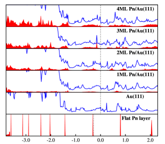
Electronic Structures of Pentacene Films on Flat Au(111). We calculated the densities of states (DOS) using optB86b-vdW method and presented the results in Figure 4. The bottom panel shows the calculated DOS of 1 ML Pen without the Au(111) slab. In-plane Pens have very well localized states with negligibly small dispersion in the form of sharp peaks due to weak overlap of the molecular orbitals. The Fermi level is chosen as the energy of the highest occupied state. The zero of the energy scale is determined with respect to Fermi energy of the bare Au(111) surface. The HOMO and the LUMO levels of Pen are identified as -0.36 eV and 0.79 eV relative to the Fermi energy. Therefore, the band gap of Pen is predicted as 1.15 eV which smaller than the experimental value of 1.85 eV.12, 36 This is a well-known underestimation of DFT due to the lack of proper cancellation of self-interaction between the Hartree and the exchange terms. In other words, standard XC functionals are not formulated to grasp the excitation processes in materials. Therefore, the unoccupied states are not properly described. This also applies to the vdW corrected DFT.
The DOS plot of 1 ML Pen on Au(111) is shown in the third panel from the bottom in Figure 4. The shades corresponding to the Pen contribution to the electronic structure of the combined system show almost no shift in energy when compared with the flat Pen layer in the absence of the gold slab. The weak coupling between the Pen contact layer and the gold surface is emphasized by the broadening of the molecular energy levels of Pen molecules over a small number of gold states. Therefore, the PDOS of the contact layer exhibits the characteristics of a film phase with its frontier molecular states contributing to the electronic structure of the combined system around the Fermi energy.
In the case of multilayers, PDOS satellites form and localize at around the flat Pn layer peak positions. Therefore, vdW-DF calculations indicate a relatively stronger molecular orbital overlap between the in-plane pentacenes in the same layer. The broadening of these satellite structures gets larger with increasing number of full monolayers. One of the main factors is associated with the long range correlation effects and is coming from the coupling between the molecules at different layers. In particular, the Pen contribution in the case of 4ML Pn/Au(111) system reflect a thin film formation. The positions of the highest occupied and lowest unoccupied states of -stacked pentacenes with respect to the Fermi energy of the metal surface show no electronic band transport feature. However, the multilayer structures organize in a well ordered thin film phase leading to a large -conjugation length along the molecular axis due to the overlap of the molecular orbitals between the nearest neighbor pentacenes. Therefore, the charge carrier transport can be explained as a result of a hopping mechanism between the localized Pen states.
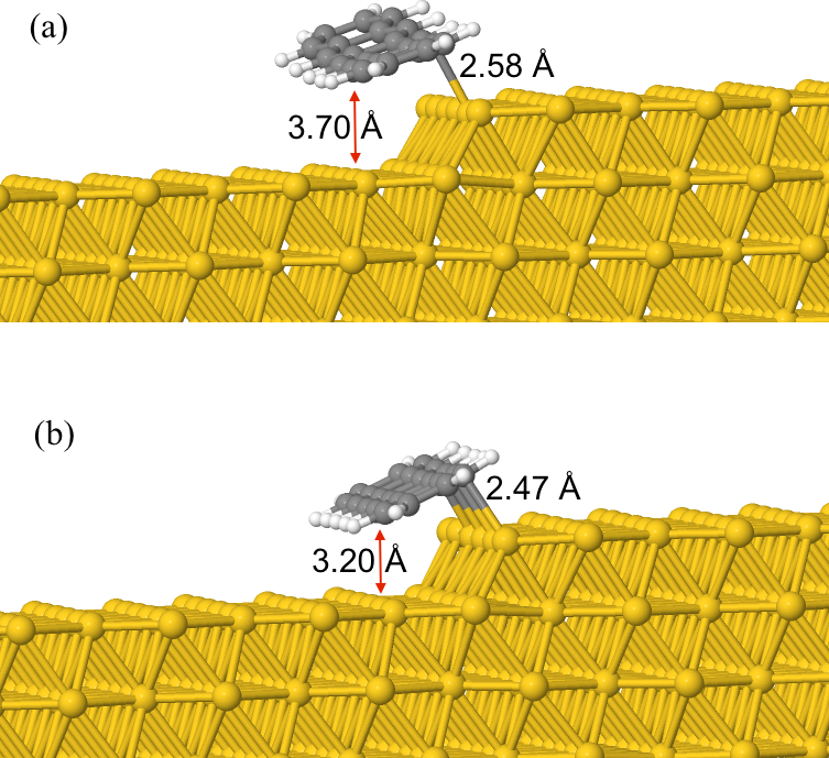
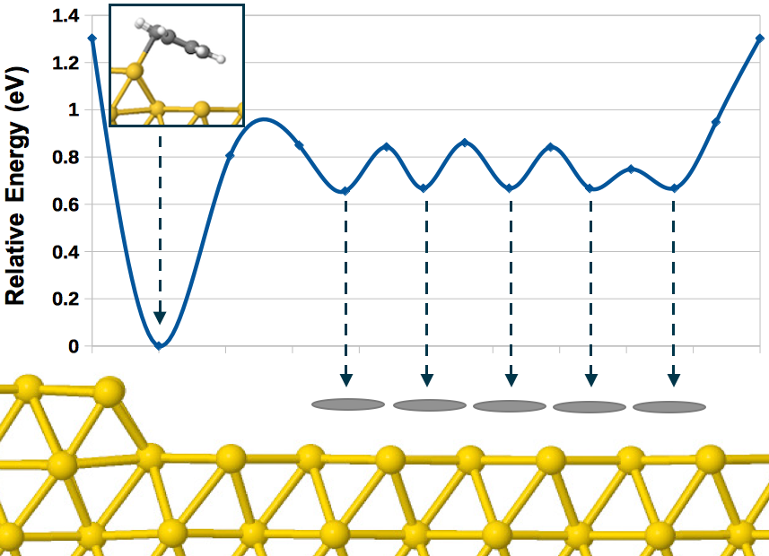
Isolated Pentacene on Vicinal Gold. We considered an isolated Pen molecule on Au(455) cell on the terrace and at the step edge with probable adsorption configurations. The initial geometries on the terrace were optimized using both PBE and optB86b-vdW methods. The results come out almost identical to those of flat Au(111) surface as tabulated in Table 1. Therefore, the low energy adsorption on the terrace turns out to be the hollow site. Then, we performed structural optimization of a single Pen molecule at the step edge using both the standard DFT and the vdW-DF calculations. The molecule at the step edge gets tilted about its major axis with respect to the Au(111) plane normal as shown in Figure 5. The tilting angle is calculated as 20.6∘ and 26.4∘ with PBE and opt86b-vdW exchange-correlation schemes, respectively. The adsorption of a single Pen at the step edge is remarkably stronger in comparison to that on the flat terrace. Then, we obtained the diffusion barrier profile of a Pen along [11] direction using the self-consistent optB86b-vdW approach. The plot in Figure 6 has been drawn by calculating the total energy of the system where the adsorbate molecule is placed at different locations along the line perpendicular to the step row on the Au(455) slab. The minimum of the potential occurs for the tilted@step geometry. The energy is 0.67 eV lower than flat@hollow adsorption at the optB86b-vdW level of theory. This difference turns out to be only 0.32 eV using the PBE XC functional as presented in Table 4. The local minima over the terrace are due to the adsorption at the hollow site. The barrier heights between two successive hollow sites correspond to the bridge-60 configuration with a value of 0.19 eV.
The relaxation of an isolated Pen at the step with the two methods brings some important structural differences as seen in Figure 5. When we use the standard PBE XC functional, the shortest bond between the molecule and an Au atom at the step edge is found to be 2.58 Å at a height of 3.70 Å from the surface plane with a significant convex bending. However, vdW-DF approach leads to even shorter and four bonds almost equal in length (2.47 Å). This time, Pen stays 3.20 Å above the gold surface and is perfectly planar. The binding energy of a single Pen molecule at the step edge is calculated using the PBE XC functional and the optB86b-vdW method as 0.65 eV (63 kJ/mol) and 2.28 eV (220 kJ/mol), respectively. The inclusion of weak dispersive interactions cause a remarkable difference in the adsorption characteristics of Pen molecules on the vicinal gold surfaces.
| Coverage | Model | PBE | optB86b-vdW | ||
|---|---|---|---|---|---|
| Et (eV) | (Å) | Et (eV) | (Å) | ||
| single | flat@hollow | 0.322 | 3.87 | 0.668 | 3.12 |
| tilted@step | 0.000 | 3.70 (2.58) | 0.000 | 3.20 (2.47) | |
| 1 ML | flat | 0.370 | 3.99 | 0.755 | 3.20 |
| flat2 | 0.083 | 3.96 | 0.000 | 3.18 | |
| tilted | 0.000 | 3.92 | “flat2” | ||
| 2 ML | flat-tilted | 0.374 | 3.79 | 1.266 | 3.10 |
| flat2-tilted | “tilted-tilted” | 0.000 | 3.06 | ||
| tilted-tilted | 0.000 | 3.29 | “flat2-tilted” | ||
Pentacene Multilayers on Vicinal Au(455). Several initial configurations have been considered to optimize a full Pen monolayer coverage on the vicinal surface using both the standard and vdW corrected DFT. These involve tilted, flat and flat2 cases. The tilted case corresponds to the model where all molecules are tilted with respect to the surface normal about their major axes. In the flat one, every Pen lays parallel over the surface as that on the planar Au(111) case. The flat2 model was constructed such that the molecules lie planar on the terrace and tilted at the step edge.
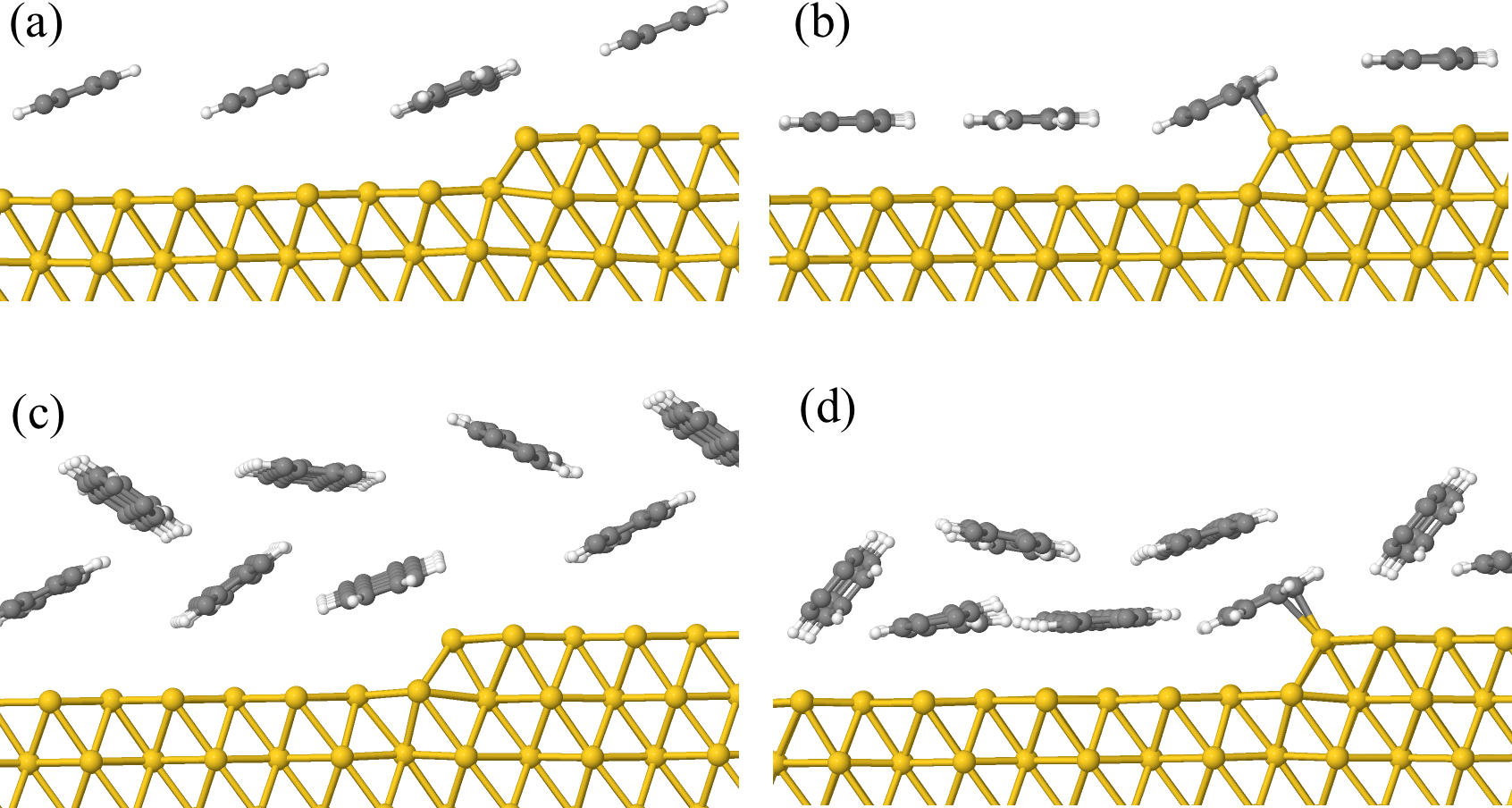
The minimum energy geometry of a full Pen monolayer on the vicinal Au surface with the standard DFT (PBE) turns out to be the tilted configuration as shown in Figure 7a. The tilting angle is about 22.8∘. Apparently, this result is different from the case of 1 ML on the flat Au(111) surface. Although the binding energy of a tilted Pen at the step edge is underestimated by PBE, the molecules on the terrace follow this tilting since intermolecular coupling is relatively stronger than the metal-molecule interaction at this level of theory. However, the vdW-DF calculations (optB86b-vdW) favor the flat2 case (Figure 7b) as a result of the inclusion of the dispersive forces self-consistently. This improves the description of organic molecule-metal surface interaction. For instance, when started from the tilted model as the initial geometry, the vdW calculations ends up with the flat2 configuration. Moreover, as presented in Table 4, the height of the adlayer from the terrace gets slightly larger than the separation of a single isolated molecule from the surface, mimicking the role of molecular orbital overlap.
The PBE XC functional follows the same trend and optimizes 2 ML Pen into tilted-tilted configuration (Figure 7c). The interaction between the Pen films and the gold surface estimated by the standard DFT is weaker than what is experimentally observed. This shortcoming of LDA parametrization of long range correlations is also implied by the calculated layer heights from the surface being unreasonably large. For instance, for the 1 ML case, PBE results in a Pen layer which stays 3.92 Å above the surface in the tilted geometry. This distance is predicted to be 3.18 Å in the flat2 model relaxed using the optB86b-vdW approach. Moreover, at the PBE level, the presence of the step does not seem to cause significant disorder in the formation of thin pentacene films on gold. On the contrary, tilted Pentacene at the step edge acts as a mediator of molecular tilting throughout the first and the second adlayers. Indeed, when we start with the flat2-tilted initial configuration, the geometry optimization with PBE XC functional resulted in the tilted-tilted model structure as indicated in Table 4. On the other hand, the vdW-DF theory of the van der Waals interactions leads to a relatively less ordered flat2-tilted formation (Figure 7d). Furthermore, optB86b-vdW relaxes the tilted-tilted configuration, which is favored by PBE, to flat2-tilted model as the minimum energy structure. When one compares the 2 ML Pen adsorption results on the flat Au(111) and on the vicinal Au(455) surface, the effect of the step becomes vital in the formation of thin film formation. Especially, vdW corrected DFT indicates disorder to a certain extent in the vicinity of the step edge.
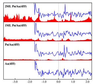
Electronically, we computed the DOS structures of the thin Pen films up to 2 ML coverage using the optB86b-vdW approach. The densities of states of the bare and a single Pen adsorbed Au(455) surfaces are depicted in the bottom two panels of Figure 8. An isolated Pen at the step exhibits significant electronic contribution at and around the Fermi energy as a result of the formation of four strong bonds with the Au atoms at the edge. The HOMO level of tilted Pen at the step is identified as eV while its LUMO lies 0.35 eV above the Fermi energy. Core molecular orbitals strongly resonate with the deeper lying gold states.
The positions of the HOMO and the LUMO levels of Pen with respect to the Fermi energy in the vicinal Au(455) surface case (Figure 8) are significantly red shifted relative to those in the flat Au(111) surface case (Figure 4). This level shift is approximately 0.4 eV. Moreover, Pen shows a larger dispersion of molecular orbitals over Au(455) states. These results indicate an enhanced charge carrier transport at the Pen-gold interface in favor of the vicinal surface.
4 Conclusions
We have performed density functional theory calculation of pentacene films with and without dispersion corrections and investigated the evolution of crystal and electronic structure of the films as a function of coverage and surface steps. To study the effects of dispersion interactions we have used a self-consistent implementation of the vdW-DF method of Dion et al. as implemented in VASP and compared the results with those obtained by the standard PBE functional. While for isolated molecules both methods yield the same adsorption site as the most preferred one for a lying down molecule, the binding strength was observed to be higher with dispersion correction as expected. The energy difference between the different binding sites were very small resulting in a smooth potential energy surface for an isolated pentacene on Au(111). Three different experimentally observed unit cell structures were investigated and (6x3) was found to be the most stable one, though the binding energies for all three were very close to each other, the difference being less than 8 kJ/mol. These results in fact explain why pentacene has so many monolayer phases/structures forming simultaneously on the Au(111) surface. While dispersion corrected results favor a flat lying first layer for all the coverages on the (111) surface, the PBE results indicate a tilting of the molecules about their long axis which is not more than 10 degrees. These results are also in agreement with the experimental findings regarding pentacene monolayer films on Au(111) which report the molecules to be either flat or to have a very small tilt angle. In case of the vicinal (455) surface, an isolated pentacene molecule was found to be strongly bound to the step edge which also causes significant contribution to the density of states at and around the Fermi energy. Dispersion corrected projected DOS calculations indicate that for the multilayer films pentacene states are significantly shifted and dispersed on the (455) surface when compared with the (111) surface, which can result in an enhanced charge transfer at the Pen-gold interface. In summary, our results underline the importance of the dispersion corrections for the loosely bound systems like pentacene on gold and the role played by step edges in determining the multilayer film structure and charge transfer at the organic molecule-metal interface.
References
- 1 Coropceanu, V.; Li, H.; Winget, P.; Zhu, L. Y.; Bredas, J.L. Electronic-Structure Theory of Organic Semiconductors: Charge-Transport Parameters and Metal/Organic Interfaces. Annu. Rev. Mater. Res., 2013, 43, 63-87.
- 2 Klauk, H. Organic thin-film transistors. Chem. Soc. Rev. 2010, 39, 2643-2666.
- 3 Wang, C. L.; Dong, H. L.; Hu, W. P.; Liu, Y. Q.; Zhu, D. B. Semiconducting -Conjugated Systems in Field-Effect Transistors: A Material Odyssey of Organic Electronics. Chem. Rev. 2012, 112, 2208-2267.
- 4 Facchetti, A. Semiconductors for Organic Transistors. Mater. Today 2007, 10, 28-37.
- 5 Ruiz, R.; Choudhary, D.; Nickel, B.; Toccoli, T.; Chang, K.-C.; Mayer, A. C.; Clancy, P.; Blakely, J. M.; Headrick, R. L.; Iannotta, S.; Malliaras, G. G. Pentacene Thin Film Growth. Chem. Mater. 2004, 16, 4497-4508.
- 6 Anthony, J.E. The Larger Acenes: Versatile Organic Semiconductors. Angew. Chem. Intl. Ed. 2008, 47, 452-483.
- 7 Casalis, L.; Danisman, M. F.; Nickel, B.; Bracco, G.; Toccoli, T.; Iannotta, S.; Scoles, G. Hyperthermal Molecular Beam Deposition of Highly Ordered Organic Thin Films. Phys. Rev. Lett. 2003, 90, 206101.
- 8 Danisman, M. F.; Casalis, L.; Scoles, G. Supersonic Molecular Beam Deposition of Pentacene Thin Films on Two Ag(111) Surfaces with Different Step Densities. Phys. Rev. B 2005, 72, 085404.
- 9 Albayrak, E.; Danisman, M. F. Helium Diffraction Study of Pentacene Films on Au(111) Appl. Surf. Sci. 2014, 295, 54-58.
- 10 France, C. B.; Schroeder, P. G.; Parkinson, B. A. Direct Observation of a Widely Spaced Periodic Row Structure at the Pentacene/Au(111) Interface Using Scanning Tunneling Microscopy. Nano Lett. 2002, 2, 693-696.
- 11 France, C. B.; Schroeder, P. G.; Forsythe, J. C.; Parkinson, B. A. Scanning Tunneling Microscopy Study of the Coverage-Dependent Structures of Pentacene on Au(111). Langmuir 2003, 19, 1274-1281.
- 12 Schroeder, P. G.; France, C. B.; Park, J. B.; Parkinson, B. A. Orbital Alignment and Morphology of Pentacene Deposited on Au(111) and SnS2 Studied Using Photoemission Spectroscopy. Journal of Physical Chemistry B 2003, 107, 2253-2261.
- 13 France, C. B.; Frame, A.; Parkinson, B. A. Electronic structure and ordering of aromatic molecules on Au(111). Proc. SPIE 5513, Physical Chemistry of Interfaces and Nanomaterials III 2004, pp.165-173.
- 14 Kang, J. H.; Zhu, X. Y. Pi-stacked Pentacene Thin Films Grown on Au(111). Appl. Phys. Lett. 2003, 82, 3248-3250.
- 15 Kang, J. H.; Zhu, X. Y. Layer-by-Layer Growth of Incommensurate, Polycrystalline, Lying-Down Pentacene Thin Films on Au(111). Chem. Mater. 2006, 18, 1318-1323.
- 16 Käfer, D.; Ruppel, L.; Witte, G. Growth of Pentacene on Clean and Modified Gold Surfaces. Phys. Rev. B 2007, 75, 085309.
- 17 Pedio, M.; Doyle, B.; Mahne, N.; Giglia, A.; Borgatti, F.; Nannarone, S.; Henze, S.K.M.; Temirov, R.; Tautz, F.S.; Casalis, L.; Hudej, R.; Danisman, M. F.; Nickel, B. Growth of Pentacene on Ag(111) Surface: A NEXAFS Study. Appl. Surf. Sci. 2007, 254, 103-107.
- 18 Dougherty, D. B.; Jin, W.; Cullen, W. G.; Reutt-Robey, J. E.; Robey, S. W. Variable Temperature Scanning Tunneling Microscopy of Pentacene Monolayer and Bilayer Phases on Ag(111). J. Phys. Chem. C 2008, 112, 20334-20339.
- 19 Duhm, S.; Bürker, C.; Niederhausen, J.; Salzmann, I.; Hosokai, T.; Duvernay, J.; Kera, S.; Schreiber, F.; Koch, N.; Ueno, N. Pentacene on Ag(111): Correlation of Bonding Distance with Intermolecular Interaction and Order. ACS Appl. Mater. Interfaces 2013, 5, 9377-9381.
- 20 Müller, K.; Seitsonen, A. P.; Brugger, T.; Westover, J.; Greber, T.; Jung, T.; Kara, A. Electronic Structure of an Organic/Metal Interface: Pentacene/Cu(110). J. Phys. Chem. C 2012, 116, 23465-23471.
- 21 Pieczyrak, B.; Abad, E.; Flores, F.; Ortega, J. Charging Energy and Barrier Height of Pentacene on Au(111): A Local-Orbital Hybrid-Functional Density Functional Theory Approach. J. Chem. Phys. 2011, 135(8), 084702.
- 22 Li, H.; Duan, Y. Q.; Coropceanu, V.; Bredas, J.-L. Electronic Structure of the Pentacene-Gold Interface: A Density-Functional Theory Study. Org. Electr. 2009, 10, 1571-1578.
- 23 Toyoda, K.; Hamada, I.; Lee, K.; Yanagisawa, S.; Morikawa, Y. Density Functional Theoretical Study of Pentacene/Noble Metal Interfaces with van der Waals Corrections: Vacuum Level Shifts and Electronic Structures. J. Chem. Phys. 2010, 132, 134703.
- 24 Wheeler, W. D.; Parkinson, B. A.; Dahnovsky, Y. The Adsorption Energy and Diffusion of a Pentacene Molecule on a Gold Surface. J. Chem. Phys. 2011, 135, 024702.
- 25 Schatschneider, B.; Monaco, S.; Tkatchenko, A.; Liang, J.J. Understanding the Structure and Electronic Properties of Molecular Crystals Under Pressure: Application of Dispersion Corrected DFT to Oligoacenes. J. Phys. Chem. A 2013, 117, 8323-8331.
- 26 Mete, E.; Demiroğlu, İ.; Danışman, M. F.; Ellialtıoğlu, Ş. Pentacene Multilayers on Ag(111) Surface. J. Phys. Chem. C 2010, 114, 2724-2729.
- 27 Mete, E.; Demiroglu, İ.; Albayrak, E.; Bracco, G.; Elliatıoğlu, Ş.; Danışman, M. F. Influence of Steps on the Tilting and Adsorption Dynamics of Ordered Pentacene Films on Vicinal Ag(111) Surfaces. J. Phys. Chem. C 2012, 116, 19429-19433.
- 28 Lee, K.; Yu, J. J.; Morikawa, Y.; Comparison of Localized Basis and Plane-Wave Basis for Density-Functional Calculations of Organic Molecules on Metals. Phys. Rev. B 2007, 75, 045402.
- 29 Ferretti, A.; Baldacchini, C.; Calzolari, A.; Di Felice, R.; Ruini, A.; Molinari, E.; Betti, M. G. Mixing of Electronic States in Pentacene Adsorption on Copper. Phys. Rev. Lett. 2007, 99, 046802.
- 30 Baldacchini, C.; Mariani, C.; Betti, M. G.; Vobornik, I.; Fujii, J.; Annese, E.; Rossi, G.; Ferretti, A.; Calzolari, A.; Di Felice, R. Symmetry Lowering of Pentacene Molecular States Interacting with a Cu Surface. Phys. Rev. B 2007, 76, 245430.
- 31 Simeoni, M.; Picozzi, S.; Delley, B. An ab-initio Study of Pentacene on Aluminum (100) Surface. Surf. Sci. 2004, 562, 43-52.
- 32 X. Sun, T. Suzuki, Y. Yamauchi, M. Kurahashi, Z.P. Wang, S. Entani, Surface Science 602 (2008) 1191-1198.
- 33 G. Saranya, S. Nair, V. Natarajan, P. Kolandaivel, K. Senthilkumar, Journal of Molecular Graphics & Modelling 38 (2012) 334-341.
- 34 Cantrell, R. A.; James, C.; Clancy, P. Computationally Derived Rules for Persistence of C60 Nanowires on Recumbent Pentacene Bilayers. Langmuir 2011, 27, 9944-9954.
- 35 Lee, K.; Yu, J. J. Ab initio Study of Pentacene on Au(001) Surface. Surf. Sci. 2005, 589, 8-18.
- 36 Schroeder, P. G.; France, C. B.; Park, J. B.; Parkinson, B. A. Energy Level Alignment and Two-Dimensional Structure of Pentacene on Au(111) Surfaces. J. Appl. Phys. 2002, 91, 3010-3014.
- 37 Grimme, S. Semiempirical GGA-Type Density Functional Constructed with a Long-Range Dispersion Correction. J. Comput. Chem. 2006, 27, 1787-1799.
- 38 Dion, M.; Rydberg, H.; Schröder, E.; Langreth, D. C.; Lundqvist, B.I. Van der Waals Density Functional for General Geometries. Phys. Rev. Lett. 2004, 92, 246401..
- 39 Yanai, T.; Tew, D. P.; Handy, N. C. A New Hybrid Exchange-Correlation Functional Using the Coulomb-Attenuating Method (CAM-B3LYP). Chem. Phys. Lett. 2004, 393, 51-57.
- 40 Chai, J. D.; Head-Gordon, M. Systematic Optimization of Long-Range Corrected Hybrid Density Functionals. J. Chem. Phys. 2008, 128(8), 084106.
- 41 Dappe, Y. J.; Ortega, J.; Flores, F. Intermolecular Interaction in Density Functional Theory: Application to Carbon Nanotubes and Fullerenes. Phys. Rev. B 2009, 79, 165409.
- 42 Blöchl, P. E. Projector Augmented-Wave Method. Phys. Rev. B 1994, 50, 17953.
- 43 Kresse, G.; Hafner, J. Ab initio Molecular Dynamics for Liquid Metals. Phys. Rev. B 1993, 47, 558.
- 44 Kresse, G.; Furthmüller, J. Efficient Iterative Schemes for Ab Initio Total-Energy Calculations Using a Plane-Wave Basis Set. Phys. Rev. B 1996, 54, 11169.
- 45 Klimeš, J.; Bowler, D. R.; Michaelides, A. Van der Waals Density Functionals Applied to Solids. Phys. Rev. B 2011, 83, 195131.
- 46 Kresse, G.; Joubert, J. From Ultrasoft Pseudopotentials to the Projector Augmented-Wave Method. Phys. Rev. B 1999, 59, 1758.
- 47 Wyckhoff, R. G. “Crystal Structures”, 2nd ed., Interscience Publishers, New York, 1958.
- 48 Soe, W.-H.; Manzano, C.; De Sarkar, A.; Chandrasekhar, N.; Joachim, C. Direct Observation of Molecular Orbitals of Pentacene Physisorbed on Au(111) by Scanning Tunneling Microscope. Phys. Rev. Lett. 2009, 102, 176102.