Spin-orbit interaction in InSb nanowires
Abstract
We use magnetoconductance measurements in dual-gated InSb nanowire devices together with a theoretical analysis of weak antilocalization to accurately extract spin-orbit strength. In particular, we show that magnetoconductance in our three-dimensional wires is very different compared to wires in two-dimensional electron gases. We obtain a large Rashba spin-orbit strength of corresponding to a spin-orbit energy of . These values underline the potential of InSb nanowires in the study of Majorana fermions in hybrid semiconductor-superconductor devices.
Hybrid semiconductor nanowire-superconductor devices are a promising platform for the study of topological superconductivity Alicea2012 . Such devices can host Majorana fermions Oreg2010 ; Lutchyn2010 , bound states with non-Abelian exchange statistics. The realization of a stable topological state requires an energy gap that exceeds the temperature at which experiments are performed (50 mK). The strength of the spin-orbit interaction (SOI) is the main parameter that determines the size of this topological gap Sau2012 and thus the potential of these devices for the study of Majorana fermions. The identification of nanowire devices with a strong SOI is therefore essential. This entails both performing measurements on a suitable material and device geometry as well as establishing theory to extract the SOI strength.
InSb nanowires are a natural candidate to create devices with a strong SOI, since bulk InSb has a strong SOI Winkler2003 ; Fabian2007 . Nanowires have been used in several experiments that showed the first signatures of Majorana fermions Mourik2012 ; Das2012 ; Deng2012 ; Churchill2013 . Nanowires are either fabricated by etching out wires in planar heterostructures or grown bottom-up. The strong confinement in the growth direction makes etched wires two-dimensional (2D) even at high density. SOI has been studied in 2D InSb wires Kallaher2010 and in planar InSb heterostructures Kallaher2010b , from which a SOI due to structural inversion asymmetry Rashba1960 , a Rashba SOI , of 0.03 eVÅ has been obtained Kallaher2010b . Bottom-up grown nanowires are three-dimensional (3D) when the Fermi wavelength is smaller than the wire diameter. In InSb wires of this type SOI has been studied by performing spectroscopy on quantum dots Nilsson2009 ; Nadj-Perge2012 , giving = 0.16 – 0.22 eVÅ Nadj-Perge2012 . However, many (proposed) topological nanowires devices Wimmer2011 ; Houzet2013 ; Hyart2013 contain extended conducting regions, i.e. conductive regions along the nanowire much longer than the nanowire diameter. The SOI strength in these extended regions has not yet been determined. It is likely different from that in quantum dots, as the difference in confinement between both geometries results in a different effective electric field and thus different Rashba SOI. Measurements of SOI strength in extended InSb nanowire regions are therefore needed to evaluate their potential for topological devices. Having chosen a nanowire material, further enhancement of Rashba SOI strength can be realized by choosing a device geometry that enhances the structural inversion asymmetry Nitta1997 ; Engels1997 . Our approach is to use a high-k dielectric in combination with a top gate that covers the InSb nanowire.
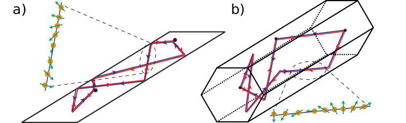
The standard method to extract SOI strength in extended regions is through low-field magnetoconductance (MC) measurements Hikami1980 ; Iordanskii1994 . Quantum interference (see Fig. 1) in the presence of a strong SOI results in an increased conductance, called weak anti-localization (WAL) Bergmann1984 , that reduces to its classical value when a magnetic field is applied Altshuler1981 . From fits of MC data to theory a spin relaxation length is extracted. If spin relaxation results from inversion asymmetry a spin precession length and SOI strength can be defined. To extract SOI strength in nanowires the theory should contain (1) the length over which the electron dephases in the presence of a magnetic field, the magnetic dephasing length Beenakker1988 , and (2) the relation between spin relaxation and spin precession length Kettemann2007 . The magnetic dephasing and spin relaxation length depend, besides magnetic field and SOI strength respectively, on dimensionality and confinement. For instance, in nanowires, the spin relaxation length increases when the wire diameter is smaller than the spin precession length Kiselev2000 ; Schapers2006 ; Kettemann2007 . Therefore the spin relaxation length extracted from WAL is not a direct measure of SOI strength. These effects have been studied in 2D wires Beenakker1988 ; Kettemann2007 , but results for 3D wires are lacking. As geometry and dimensionality are different (see Fig. 1), using 2D results for 3D wires is unreliable. Thus, theory for 3D wires has to be developed.
In this Letter, we first theoretically study both magnetic dephasing and spin relaxation due to Rashba SOI in 3D hexagonal nanowires. We then use this theory to determine the spin-orbit strength from our measurements of WAL in dual-gate InSb nanowire devices, finding a strong Rashba SOI = .
The WAL correction to the classical conductivity can be computed in the quasiclassical theory as Chakravarty86 ; Beenakker1988 ; Kurdak92
| (1) |
The length scales in this expression are the nanowire length , the mean free path , the phase coherence length , the magnetic dephasing length , and the spin relaxation length . The mean free path where is the mean time between scattering events and the Fermi velocity. In addition, the remaining length scales are also related to corresponding time scales as
| (2) |
where the diffusion constant in dimensions ( for bottom-up grown nanowires).
In the quasiclassical theory, (and hence ) is a phenomenological parameter. In contrast, and are computed from a microscopic Hamiltonian, by averaging the quantum mechanical propagator over classical trajectories (a summary of the quasiclassical theory is given in the supplemental material SI ). and thus depend not only on microscopic parameters (magnetic field and SOI strength, respectively), but through the average over trajectories also on dimensionality, confinement, and . We focus on the case where Rashba SOI due to an effective electric field in the -direction, perpendicular to wire and substrate, dominates. Then the microscopic SOI Hamiltonian is , where are Pauli matrices and the momentum operators. The corresponding spin-orbit precession length, , equals . In our treatment we neglect the Zeeman splitting, since we concentrate on the regime of large Fermi wave vector, , such that .
The quasiclassical description is valid if the Fermi wave length , and much smaller than the transverse extent of the nanowire, i.e. for many occupied subbands. In particular, the quasiclassical method remains valid even if Zaitsev05 . Additional requirements are given in SI .
We evaluate and numerically by averaging over random classical paths for a given nanowire geometry. The paths consist of piece-wise linear segments of freely moving electrons with constant speed Chakravarty86 ; Beenakker91 , only scattered randomly from impurities and specularly at the boundary (for numerical details see SI ). These assumptions imply a uniform electron density in the nanowire. Specular boundary reflection is expected as our wires have no surface roughness Xu2012 .
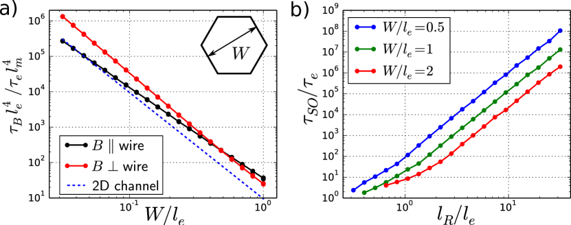
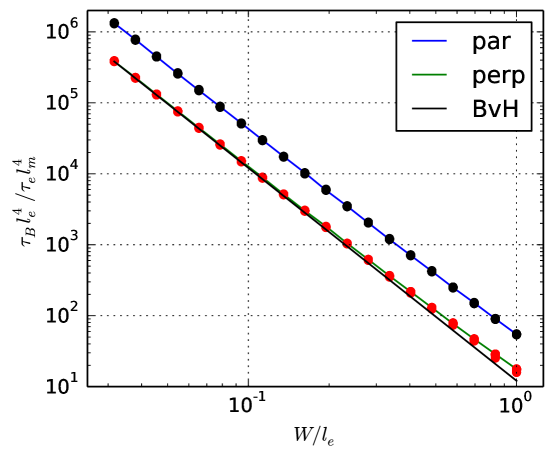
We apply our theory to nanowires with a hexagonal cross-section and diameter (see inset in Fig. 2(a)) in the quasi-ballistic regime, . Fig. 2(a) shows the magnetic dephasing time (normalized by with ) as a function of wire diameter. Both parallel and perpendicular field give rise to magnetic dephasing due to the three-dimensionality of the electron paths, in contrast to two-dimensional systems where only a perpendicular field is relevant (see Fig. 1). The different field directions show a different dependence on , with, remarkably, (and thus ) independent of field-orientation for . Our results for as a function of are shown in Fig. 2(b). We find an increase of as the wire diameter is decreased, indicating that confinement leads to increased spin relaxation times.
For we can fit our results reliably as
| (3) |
This is shown for in Fig. 2(a) where data for different and collapse to one line. In particular for , we find and for parallel field, and for perpendicular field. For and . Note that our numerics is valid beyond the range where the fit (3) is applicable. For example, for the numerical result deviates from the power-law of (3) as seen in Fig. 2(b); in this regime only the numerical result can be used.
The fit (3) allows for a quantitative comparison of our 3D wire results to 2D wires: Both are similar in that there is flux cancellation () Beenakker1988 and suppressed spin relaxation due to confinement. However, they exhibit a significantly different power-law. As an example, in Fig. 2(a) we compare to the 2D wire result for weak fields from Beenakker1988 (, ) that can differ by an order of magnitude from our results. This emphasizes the need for an accurate description of geometry for a quantitative analysis of WAL.
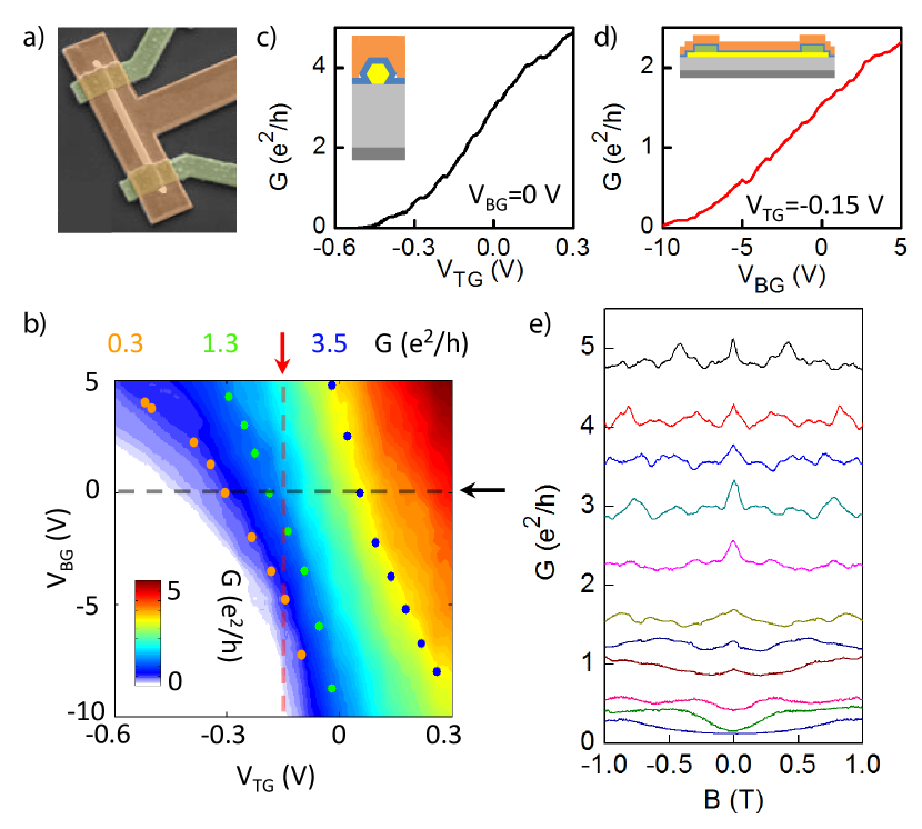
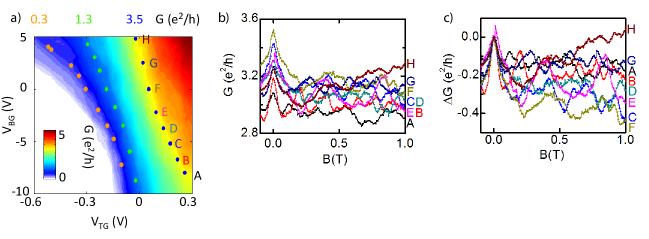
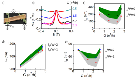
We continue with the experiment. InSb nanowires Plissard2012 with diameter are deposited onto a substrate with a global back gate. A large () contact separation ensures sufficient scattering between source and drain. After contact deposition a HfO2 dielectric layer is deposited and the device is then covered by metal, creating an -shaped top gate (Fig. 3a and insets of Fig. 3c-d). Nanowire conductance is controlled with top and back gate voltage, reaching a conductance up to (Fig. 3b). The device design leads to a strong top gate coupling (Fig. 3c), while back gate coupling is weaker (Fig. 3d). From a field-effect mobility of a ratio of mean free path to wire diameter is estimated SI ; Plissard2013 .
At large the magnetoconductance, measured with conductance controlled by the top gate at a temperature and with perpendicular to the nanowire and substrate plane, shows an increase of conductance of 0.2 to around (Fig. 3(e)). () is, apart from reproducible conducantance fluctuations, flat at 200 mT, which is further evidence of specular boundary scattering Beenakker91 . On reducing conductance below WAL becomes less pronounced and a crossover to WL is seen.
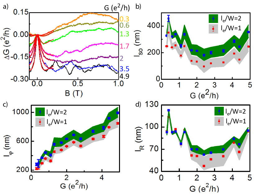
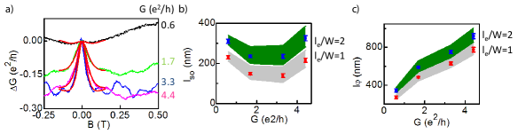
Reproducible conductance fluctuations, most clearly seen at larger (Fig. 3(e)), affect the WAL peak shape. To suppress these fluctuations several () MC traces are taken at the same device conductance (see Fig. 3(b)). After averaging these traces WAL remains while the conductance fluctuations are greatly suppressed (Fig. 4(a)). Also here on reduction of conductance a crossover from WAL to WL is seen. Very similar results are obtained when averaging MC traces obtained as a function of top gate voltage with SI . We expect that several () subbands are occupied at device conductance (see SI ). Hence, our quasiclassical approach is valid and we fit the averaged MC traces to Eq. (Spin-orbit interaction in InSb nanowires) with , and the conductance at large magnetic field as fit parameters. is extracted from Eq. (3). Wire diameter and mean free path are fixed in each fit, but we extract fit results for a wire diameter deviating from its expected value and for both and . We find good agreement between data and fits (see Fig. 4(a)). While showing fit results covering the full range of , we base our conclusions on results obtained in the quasiclassical transport regime 2e2/h.
On increasing conductance, the spin relaxation length first decreases to , then increases again to when (Fig. 4(b)). The phase coherence length (Fig. 4(c)) shows a monotonous increase with device conductance. This increase can be explained by the density dependence of either the diffusion constant or the electron-electron interaction strength Lin2002 , often reported as the dominant source of dephasing in nanowires Liang2012 ; Kallaher2010 .
Spin relaxation Wu2010 in our device can possibly occur via the Elliot-Yafet ElliotYafet1963 or the D’yakonov-Perel’ mechanism Dyakanov1972 , corresponding to spin randomization at or in between scattering events, respectively. The Elliot-Yafet contribution can be estimated as Chazalviel1975 , with band gap , Fermi energy , spin-orbit gap and . For the D’yakonov-Perel’ mechanism, we note that our nanowires have a zinc-blende crystal structure, grown in the [111] direction, where Dresselhaus SOI is absent for momentum along the nanowire footnote_dresselhaus . We therefore expect that Rashba SOI is the dominant source of spin relaxation, in agreement with previous experiments Nadj-Perge2012 . As found in our theoretical analysis, it is then crucial to capture confinement effects accurately. Our correspond to 2 – 15 that are captured well by our simulations footnote1 . Given that , we extract the corresponding to our directly from Fig. 2(b). We extract spin precession lengths of , shown in Fig. 4(d), corresponding to . MC measurements on a second device show very similar SI .
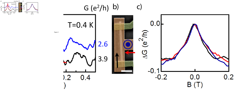
To confirm the interpretation of our MC measurements we extract MC at a lower temperature (Fig. 5a). We find larger WAL amplitudes of up to , while the width of the WAL peak remains approximately the same as at , corresponding to a longer at lower temperature, with approximately constant . A longer is expected at lower temperature, as the rate of inelastic scattering, responsible for loss of phase coherence, is reduced in this regime.
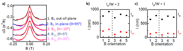
Our theoretical analysis found similar dephasing times for magnetic fields perpendicular and parallel to the nanowire for our estimated mean free paths, . Indeed, we observe virtually identical WAL for fields parallel and perpendicular to the nanowire in our second device (see Figs. 5(b)-(c)). WAL in the first device is also very similar for both field directions SI . This is in striking contrast to MC measurements in two-dimensional systems where only a perpendicular magnetic field gives strong dephasing due to orbital effects. It also provides strong support for the assumptions made in our theory, and emphasizes the importance of including the three-dimensional nature of nanowires to understand their MC properties. In contrast, WL is anisotropic SI , which we attribute to a different density distribution at low conductance compared to the high conductance at which WAL is seen.
Relevant to Majorana fermion experiments is the spin-orbit energy, , that is in our devices. These values compare favorably to InAs nanowires that yield Liang2012 ; Hansen2005 and corresponding . is similar or slightly larger than reported spin-orbit energies in Ge/Si core-shell nanowires ( Hao2010 ), while is larger than ). Note that the device geometries and expressions for () used by different authors vary and that often only , not is evaluated. With our we then find, following the analysis of Ref. Sau2012 , a topological gap of SI even for our moderate mobilities of order . This gap largely exceeds the temperature and previous estimates. Hence, our findings underline the potential of InSb nanowires in the study of Majorana fermions.
We thank C. M. Marcus, P. Wenk, K. Richter and I. Adagideli for discussions. Financial support for this work is provided by the Dutch Organisation for Scientific Research (NWO), the Foundation for Fundamental Research on Matter (FOM) and Microsoft Corporation Station Q. V. S. P. acknowledges funding from NWO through a Veni grant.
References
- (1) J. Alicea, Rep. Prog. Phys. 75, 076501 (2012).
- (2) Y. Oreg, G. Refael, F. von Oppen, Phys. Rev. Lett. 105, 177002 (2010).
- (3) R. M. Lutchyn, J. D. Sau, S. Das Sarma, Phys. Rev. Lett. 105, 077001 (2010).
- (4) J. D. Sau, S. Tewari, S. Das Sarma, Phys. Rev. B 85, 064512 (2012).
- (5) R. Winkler, Spin-orbit coupling effects in two-dimensional electron and hole systems, Springer Berlin, Heidelberg (2003).
- (6) J. Fabian, A. Matos-Abiague, C. Ertler, P. Stano, I. Zutic, Acta Phys. Slov. 57, 565-907 (2007).
- (7) V. Mourik, K. Zuo, S. M. Frolov, S. R. Plissard, E. P. A. M. Bakkers, and L. P. Kouwenhoven, Science 336, 1003 (2012).
- (8) A. Das, Y. Ronen, Y. Most, Y. Oreg, M. Heiblum, and H. Shtrikman, Nat. Phys. 8, 887 (2012).
- (9) M. T Deng, C. L. Yu, G. Y. Huang, M. Larsson, P. Caroff, and H. Q. Xu, Nano Lett. 12, 6414 (2012).
- (10) H. O. H. Churchill, V. Fatemi, K. Grove-Rasmussen, M. T. Deng, P. Caroff, H. Q. Xu, and C. M. Marcus, Phys. Rev. B 87, 241401(R) (2013).
- (11) R. L. Kallaher, J. J. Heremans, N. Goel, S. J. Chung, M. B. Santos, Phys. Rev. B 81, 035335 (2010).
- (12) R. L. Kallaher, J. J. Heremans, N. Goel, S. J. Chung, M. B. Santos, Phys. Rev. B 81, 075303 (2010).
- (13) E. I. Rashba, Soviet Phys. Semicond. 2, 1109 (1960).
- (14) H. A. Nilsson, P. Caroff, C. Thelander, M. Larsson, J. B. Wagner, L.-E. Wernersson, L. Samuelson, H. Q. Xu, Nano Lett. 9, 3151 (2009).
- (15) S. Nadj-Perge, V. S. Pribiag, J. W. G. van den Berg, K. Zuo, S. R. Plissard, E. P. A. M. Bakkers, S. M. Frolov, and L. P. Kouwenhoven, Phys. Rev. Lett. 108, 166801 (2012).
- (16) M. Wimmer, A. R. Akhmerov, J. P. Dahlhaus, and C. W. J. Beenakker, New J. Phys. 13, 053016 (2011).
- (17) M. Houzet, J. S. Meyer, D. M. Badiane, L. I. Glazman, Phys. Rev. Lett. 111, 046401 (2013).
- (18) T. Hyart, B. van Heck, I. C. Fulga, M. Burrello, A. R. Akhmerov, and C W. J. Beenakker, Phys. Rev. B 88, 035121 (2013).
- (19) J. Nitta, T. Akazaki, H. Takayanagi, T. Enoki, Phys. Rev. Lett. 78, 1335-1338 (1997).
- (20) G. Engels, J. Lange, T. Schäpers, H. Lüth, Phys. Rev. B 55, R1958-R1961 (1997).
- (21) S. Hikami, A. I. Larkin, Y. Nagaoka, Progr. Theor. Phys. 63, 2, 707 (1980)
- (22) S. Iordanskii, Y. Lyanda-Geller and G. Pikus, JETP Lett. 60, 206-211 (1994).
- (23) G. Bergmann, Phys. Rep. 107, 1-58 (1984).
- (24) B. L. Al’tshuler, A. G. Aronov, A. I. Larkin, D. E. Khmel’nitskii, JETP Lett. 54(2) (1981).
- (25) C. W. .J. Beenakker and H. van Houten, Phys. Rev. B. 38, 3232-3240 (1988).
- (26) S. Kettemann, Phys. Rev. Lett. 98, 176808 (2007).
- (27) A. A. Kiselev and K. W. Kim, Phys. Rev. B 61, 13115 (2000).
- (28) T. Schäpers, V. A. Guzenko, M. G. Pala, U. Zülicke, M. Governale, J. Knobbe, and H. Hardtdegen, Phys. Rev. B 74, 081301 (2006).
- (29) S. Chakravarty, A. Schmid, Physics Reports 140, 193 (1986).
- (30) C. Kurdak, A. M. Chang, A. Chin, T. Y. Chang, Phys. Rev. B 46, 6846 (1992).
- (31) O. Zaitsev, D. Frustaglia, K. Richter, Phys. Rev. B 72, 155325 (2005).
- (32) See Supplemental Material for details of the numerical simulations and additional experimental data.
- (33) S. R. Plissard, I. van Weperen, D. Car, M. A. Verheijen, G. W. G. Immink, J. Kammhuber, L. J. Cornelissen, D. B. Szombati, A. Geresdi, S. M. Frolov, L. P. Kouwenhoven, and E. P. A. M. Bakkers, Nature Nano. 8, 859-864 (2013).
- (34) C. W. J. Beenakker, H. van Houten, Solid State Physics 44, 1 (1991).
- (35) T. Xu, K. A. Dick, S. Plissard, T. H. Nguyen, Y. Makoudi, M. Berthe, J.-P. Nys, X. Wallart, B. Grandidier, and P. Caroff, Nanotechnology 23, 095702 (2012). We extrapolate the results on InAsSb wires to InSb since the flatness of the facets results from the introduction of Sb.
- (36) S. R. Plissard, D. R. Slapak, M. A. Verheijen, M. Hocevar, G. W. G. Immink, I. van Weperen, S. Nadj-Perge, S. M. Frolov, L. P. Kouwenhoven and E. P. A. M. Bakkers, Nano Lett. 12, 1794 (2012).
- (37) J. J. Lin, J. P. Bird, J. Phys.: Condens. Matt. 14, R501 (2002).
- (38) D. Liang, X. P. A. Gao, Nano Lett. 12, 3263 (2012).
- (39) M. W. Wu, J. H. Jiang and M. Q. Weng, Phys. Rep. 493, 61 (2010).
- (40) Y. Yafet, Solid State Physics vol.14, Academic Press, New York (1963); R. J. Elliott, Phys. Rev. 96, 266 (1954).
- (41) M. D’yakonov and V. Perel’, Soviet Phys. Solid State 13, 3023 (1972).
- (42) J. Chazalviel, Phys. Rev. B 11, 1555 (1975).
- (43) Furthermore, even for [100] nanowires Dresselhaus SOI is weak: In this case the maximum linear Dresselhaus SOI strength is (with the cubic Dresselhaus SOI strength), yielding a spin-orbit length . With eVÅ3 Fabian2007 and meV we estimate nm.
- (44) Exceptions are the smallest values of at and : When assuming a wire width larger than the expected value () we find . In this case the corresponding to the lowest simulated value of have been chosen as a lower bound.
- (45) A. E. Hansen, M. T. Björk, C. Fasth, C. Thelander, and L. Samuelson, Phys. Rev. B 71, 205328 (2005); P. Roulleau, T. Choi, S. Riedi, T. Heinzel, I. Shorubalko, T. Ihn, and K. Ensslin, Phys. Rev. B 81, 155449 (2010); S. Dhara, H. S. Solanki, V. Singh, A. Narayanan, P. Chaudhari, M. Gokhale, A. Bhattacharya, and M. M. Deshmukh, Phys. Rev. B 79 121311(R) (2009); S. Estévez Hernández, M. Akabori, K. Sladek, C. Volk, S. Alagha, H. Hardtdegen, M. G. Pala, N. Demarina, D. Grützmacher, and T. Schäpers, Phys. Rev. B 82, 235303 (2010).
- (46) X.-J. Hao, T. Tu, G. Cao, C. Zhou, H.-O. Li, G.-C. Guo, W. Y. Fung, Z. Ji, G.-P. Guo, and W. Lu, Nano Lett. 10, 2956 (2010); A. P. Higginbotham, F. Kuemmeth, T. W. Larsen, M. Fitzpatrick, J. Yao, H. Yan, C. M. Lieber, and C. M. Marcus Phys. Rev Lett. 112, 216806 (2014).
Appendix A Supplemental material
Appendix B 1. Summary of the quasiclassical theory
Within the quasiclassical formalism, the weak (anti)localization correction is given as suppChakravarty86 ; suppBeenakker91 ; suppKurdak92
| (4) |
In this expression, is the length of the nanowire, is the 1D return probability, the diffusion coefficient ( for the nanowires). denotes an average over all classical paths that close after time . is due to the orbital effect of the magnetic field and reads suppChakravarty86
| (5) |
The Hamiltonian of spin-orbit interaction (SOI) can in general be written as
| (6) |
where is a vector of Pauli matrices and a momentum-dependent effective magnetic field due to the SOI. In the case of Rashba SOI as considered here we have . The SOI of Eq. (6) then gives rise to the modulation factor suppChakravarty86 ; suppZaitsev05
| (7) |
where is the time-order operator.
When the motion along the longitudinal direction of wire is diffusive, the modulation factors generally decay exponentially with time suppChakravarty86 ,
| (8) |
Note that and depend explicitly on the magnetic field and the SOI strength through equations (5) and (B), respectively. However, through the average over classical paths, they also depend on the geometry of the nanowire and the mean free path .
With the exponential form of the modulation factors in Eq. (8) the integral in Eq. (4) can be performed to give the expression (1) of the conductance correction in the main text.
B.1 Requirements of the quasi-classical theory
The quasiclassical description is valid if the Fermi wave length is much smaller than the typical transverse extent of the nanowire , i.e. for many occupied subbands. It also requires that the classical paths are neither affected by magnetic field nor SOI: The former requires that the cyclotron radius suppChakravarty86 ; suppBeenakker91 , the latter that the kinetic energy dominates over the spin-orbit energy so that suppZaitsev05 . In particular, the quasiclassical method is valid also for . Additional requirements are , for the exponential decay of magnetic dephasing time (length) and spin relaxation time to be valid suppBeenakker91 ; suppZaitsev05 . In addition we must have to be in the quasi-one-dimensional limit, where the return probability in Eq. (4) is given by the 1D return probabilty.
These are the fundamental requirements for the quasiclassical theory to hold. They should not confused with the stronger requirements needed for the validity of the fit in Eq. (3) of the main text.
B.1.1 Experimental fulfilment of quasi-classical requirements
The number of occupied subbands is discussed in section 4 of this document. As shown in Fig. 4c of the main text, largely exceeds the wire diameter for a large range of conductance, thereby obeying the requirement for a one-dimensional quantum interference model. The range of (up to ) in the fits in Figs. 4-5 of the main text and in the figures in this document in general obey . Alternatively, fitting over a smaller -range (up to , fulfilling , and to a larger extent) can be performed on MC traces showing WAL without WL at larger (observed when ) with fixed , yielding the same results within 20%.
Appendix C 2. Monte Carlo evaluation of the weak (anti)localization correction.
In order to obtain the decay times in Eq. (8) as a function of mean free path , wire diameter , and magnetic field or Rashba spin-orbit strength , we performed Monte-Carlo simulations of quasiclassical paths in a hexagonal nano-wire, as has been described before in Refs. suppChakravarty86 ; suppBeenakker91 ; suppZaitsev05 .
C.1 Model and Boltzmannian ensemble
We model the nanowire as a three-dimensional prisma of infinite length, with a regular hexagon as cross-section.
A Boltzmannian ensemble of quasiclassical paths is created, with each path consisting of propagation along a sequence of straight line segments with constant velocity. For each path, after certain intervals, the direction of the particles velocity is changed at random, with isotropic distribution, corresponding to collision of randomly distributed pointlike impurities. The distance of free propagation between collision is determined at random, Poisson-distributed , so that the mean-free path is . On impact with one of the nanowires walls, reflection occurs in a specular fashion, by reversing the velocity component perpendicular to the wall. The resulting ensemble will consist of paths which are open (start and end point do not coincide).
C.2 Evaluation of ,
After obtaining an ensemble of Boltzmannian paths, for each path the integrals Eq. (5) or Eq. (B) are evaluated. Because the paths consist of straight line segments, the evaluation is elementary for each segment, and the integrals , are the products of these segments. For , these are the phase factors accumulated along each segment, while for we must multiply unitary two-by-two matrices which describe the spin dynamics along each segment. When calculating at the same time as generating the path, only the last position, velocity and accumulated product of need to be kept in memory.
C.2.1 Magnetic field
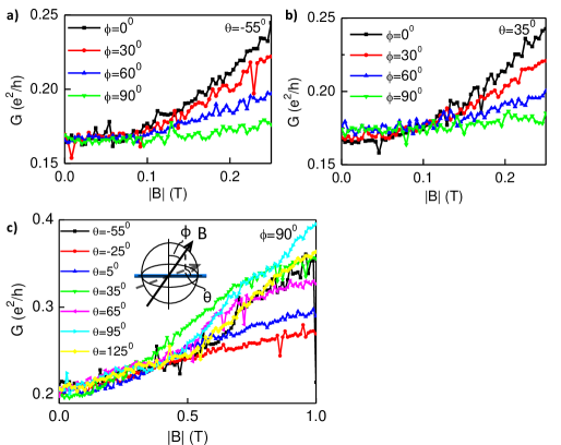
To be more specific, for magnetic fields we choose the field to point along the direction, and the nanowire to lie along either the or direction, so that the magnetic field is either perpendicular or parallel to the nanowires axis. In the perpendicular case, the orientation of the nanowire was either such that the magnetic field penetrated one of the faces perpendicularly, or such that it was parallel to one of the faces (the difference being a rotation by 30 degrees). It was established that for the resulting there is no significant difference between these two orientations in the relevant regime.
When choosing the gauge,
| (9) |
the generation of open paths is sufficient for the evaluation of according to Eq. (5), because the average over open and closed paths is then identical suppBeenakker1988 . Since open and closed paths are equivalent in this situation, we use open paths that are easier to generate numerically than closed paths. In our simulations, we chose an ensemble size of open paths to for averaging.
C.2.2 Spin-orbit
For an evaluation with open paths is not possible, and we have to average over an ensemble of closed paths, which is created as described in the following. By creating a number of open paths of length , we can create a set of statistically independent open paths of length , by pairwise concatenation of two different paths. We restrict this much larger set of paths to those which are almost closed (with start and end point separated not further than ), and then insert an additional line segment that closes these paths. If the concatenated paths are of sufficient length, we assume that the insertion of this additional line segment with a slightly different length distribution than the other line segments does not change the ensemble properties appreciably. Because we thus could only use a subset of the generated paths, we chose an ensemble size of open paths in this case. (The size of the ensemble of closed paths decreases with increasing ).
C.3 Fitting decay times
Finally, after having created ensembles of open or closed paths as described above for a set of different path lengths, which we chose to be logarithmically spaced, with integer and , we determined the averages and numerically fitted the exponential decays according to Eqs. (5) in the main text, resulting in estimates for the decay times and .
Appendix D 3. Validating the numerics against known results
D.1 Square nanowire in magnetic field
To validate the results of our simulations for , we also simulate other geometries, in which results have been found previously, numerically or analytically. First, instead of considering hexagonal nanowires, we change the shape of the nanowire to be square. If a square nanowire is placed in a perpendicular magnetic field and has specularly reflecting walls, we expect the result to be the same as for a 2D layer, as treated in suppBeenakker1988 . This is because reflections on the walls perpendicular to do not change the projection of the path along the direction of , and thus are ineffective.
We should thus reproduce the result of Ref. suppBeenakker1988 , which in the “clean, weak field” limit reads
| (10) |
and should hold for and . In Fig. S1 we show simulation results for both perpendicular and parallel field for a square nanowire. In perpendicular field, the data agrees to the analytical results in the regime of its validity (the onset of cross-over to the diffusive case can be seen). Remarkably, in parallel field, we also observe a dependence, while for hexagonal geometry, the dependence on has two different for the two orientations.
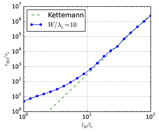
D.2 Spin-orbit coupling in 2D strip
To check the calculations of , we compare our simulations to the expression for for two-dimensional diffusive wires () with Rashba spin-orbit interaction from Kettemann suppKettemann2007 .
When comparing between different sources it is important to note that different conventions for exist (such as choosing a factor in Eq. (8)). For consistency it is thus important to compare physical observables. For weak antilocalization this is the conductance correction. In order to describe the case of diffusive wires () we need to take the limit in Eq. (1) of the main text.:
| (11) |
Kettemann uses a Green’s function based approach and arrives at suppKettemann2007 :
| (12) |
In the limit of small spin-orbit splitting, , both expressions become equal if we identify
| (13) |
Hence we need to take this factor of 2 into account when comparing our results to Kettemann’s. Taking this factor into account, the expressions (11) and (12) not only agree for weak spin-orbit, but also never differ by more than 5% for all .
Fig. S2 shows the comparison between the expression given in Ref. suppKettemann2007 , which after conversion to the quantities in this paper is
| (14) |
and numerical results we obtained for a diffusive 2D strip for different spin-orbit strengths.
Appendix E 4. Device fabrication and estimations of mobility, mean free path, wire diameter and occupied subbands
E.1 Device fabrication
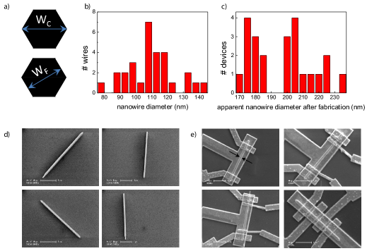
The nanowire is deposited onto a p++-doped Si substrate covered by 285 nm SiO2 (depicted in black in Fig. 3a of the main text). Contacts to the nanowire (green) are made by a lift-off process using electron beam lithography. Contact material is Ti/Au (25/125 nm). After passivation of the nanowire with a diluted ammoniumpolysulfur solution (concentration (NH4)SX:H2O 1:200) the chip is covered with HfO2 (30 nm), deposited by atomic layer deposition. The dielectric is removed at the bonding pads by the writing of an etch mask (PMMA) followed by an HF etch. A top gate (brown) is deposited using a lift-off process with electron beam lithography. Top gate is defined using Ti/Au (25/175 nm). Lastly, an additional layer of Ti/Pt (5/50 nm) is deposited on the bond pads to reduce the chance of leakage to the global back gate. Devices were only imaged optically during device fabrication. SEM imaging was performed only after the measurements.
E.2 Estimation of mobility, mean free path and
Nanowire mobility, , is obtained from pinch-off traces using the method described in section 3 of the Supplementary Material of suppPlissard2013 . In short, mobility is obtained from the change of current, or conductance, with gate voltage. We thus extract field-effect mobility, whereby we rely on a fit of the gate trace to an expression for gate-induced transport. This expression includes a fixed resistance in series with the gated nanowire.
To extract mobility and series resistances from device I (data shown in Fig. 3-5a of the main text and Fig. S3, Fig. S6, Fig. S7, Fig. S8, Fig. S9 of this document) in this way, a gate trace from pinch-off to saturation is needed. However, (, = 0 V) obtained from Fig. S3a covers only an intermediate range (see S3b). Therefore traces at (, = 0.15 V) and (, = 0.15 V), shown in Fig. S3b are also used. The three traces then together form a full pinch-off trace (see Fig. S3c) that is well approximated by Eq. 11 in suppPlissard2013 for which here an equivalent expression for current instead of conductance was used. Here the capacitance between back gate and nanowire = 22 aF, the series resistance = 10 k, the mobility = 12,500 cm2/Vs and the threshold voltage = 16.5 V (see Fig. S3c). Other inputs are source-drain bias = 10 mV and contact spacing = 2 m. The capacitance has been obtained from electrostatic simulations in which the hexagonal shape of the nanowire has been taken into account. The series resistance consists of instrumental resistances (RC-filters and ammeter impedance, together 8 k) and a contact resistance . The experimental pinch-off traces are best approximated by = 2 k. Expressions for () with = 1 k and = 3 k, also shown in Fig. S3c, deviate from the measured pinch-off traces.
Mobility is also estimated from a linear fit to the top gate pinch-off trace shown in Fig. S3d. Prior to this fit instrumental and series resistances have been subtracted. From the fit 9,000 cm2/Vs is obtained, using = 1440 aF, obtained from electrostic simulations, and = 2 m.
Similarly, mobility in device III (see Fig. S3e, magnetoconductance data shown in Fig. S10 of this supplementary document) is extracted from a fit to the top gate pinch-off trace, giving 10,000 cm2/Vs using = 1660 aF and = 2.3 m. These mobilities are similar to those obtained in InSb nanowires that are gated using only a global back gate suppPlissard2013 .
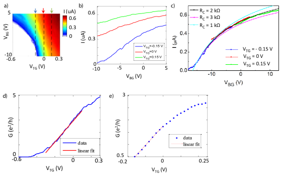
Mean free path, , is estimated as = , with the Fermi velocity and the scattering time. = , with electron charge and the effective electron mass in InSb. Assuming a 3D density of states = with the reduced Planck constant and electron density, is estimated from pinch off traces using = with the nanowire cross section, top or back gate voltage and the threshold (pinch-off) voltage. In this way in device I up to 41017 cm-3 are obtained, giving up to 160 nm. This estimate of agrees reasonably with densities obtained from a Schrödinger-Poisson solver (see ’Estimation of the number of occupied subbands’). In device III up to 41017 cm-3 gives 150 nm. Together with the facet-to-facet width (described in Fig. S4) these mean free paths yield a ratio = 1-2.
E.3 Nanowire width
Nanowires were not imaged with scanning electron microscope prior to device fabrication to avoid damage due to electron irradiation. The wire diameter is estimated from a comparison of the nanowire width after fabrication to the nanowire diameter obtained from a number of wires from the same growth batch deposited on a substrate as described in Fig. S4.
E.4 Estimation of the number of occupied subbands
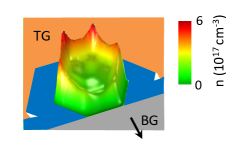
An estimate of the number of occupied subbands is calculated in two ways:
-
1.
A self-consistent Schrodinger-Poisson calculation yields that 17 subbands contribute to transport at higher device conductance (density profile shown in the inset of Fig. S5). As contact screening has been neglected in these two-dimensional calculations the actual number of subbands may be slightly lower, but likely several ( 10) modes contribute at high device conductance.
-
2.
The conductance, , of a disordered quantum wire relates to the number of subbands, , as suppBeenakker1997
(15) which, using 10 – 20 (obtained from the estimate of above) yields 25.
Appendix F 5. Supplementary experimental data
F.1 Magnetoconductance traces at constant conductance
F.2 Spin relaxation and phase coherence length obtained from top gate averaging in device I
F.3 Phase coherence and spin relaxation length at = 0.4 K
| G (e2/h) | (nm) | (nm) | |
|---|---|---|---|
| 3.9 | 1 | 95 18 | 1078 32 |
| 2 | 205 16 | 1174 39 | |
| 2.6 | 1 | 171 26 | 805 52 |
| 2 | 380 29 | 937 60 |
F.4 Magnetoconductance in parallel and perpendicular field in device I
F.5 Device III: reproducibility of extracted spin relaxation and phase coherence lengths
Appendix G 6. Topological gap as a function of mobilty and spin-orbit strength
We follow the theoretical analysis of Ref. suppSau2012 to compute the maximum topological gap that can be achieved at a given mobilty and spin-orbit strength . One should only be careful to note that the definition of in suppSau2012 differs by a factor of 4 from ours. Whenever we refer to here, we use our definition from the main text.
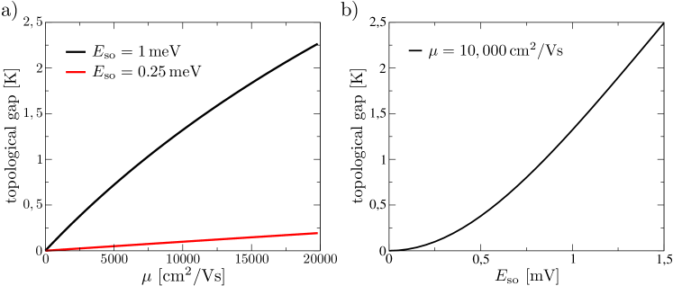
In Fig. S11a we show the topological gap as a function of mobility for the spin-orbit energies estimated in the main text, with parameters suitable for the Majorana experiments in Ref. suppMourik2012 . We observe a nearly linear dependence of the topological gap on mobility for these parameters. The topological gap can be rather sizable, and we find gaps of order for a moderate mobility of for . From the figure it is also apparent that the topological gap depends rather strongly on .
We investigate the -dependence of the topological gap in Fig. S11b. At a mobility of 10,000 cm2/Vs the topological gap depends roughly quadratically on up to , i.e. the topological gap increases as . This is in stark contrast to the clean case where the topological gap depends linearly on .
The different dependences of the topological gap on mobility (linear) and spin-orbit strength (to the fourth power) indicates that for current devices it may be more efficient to attempt to improve spin-orbit strength rather than mobility.
References
- (1) S. Chakravarty, A. Schmid, Physics Reports 140, 193 (1986).
- (2) C. W. J. Beenakker, H. van Houten, Solid State Physics 44, 1 (1991).
- (3) C. Kurdak, A. M. Chang, A. Chin, T. Y. Chang, Phys. Rev. B 46, 6846 (1992).
- (4) O. Zaitsev, D. Frustaglia, K. Richter, Phys. Rev. B 72, 155325 (2005).
- (5) C. Beenakker and H. van Houten, Phys. Rev. B. 38, 3232-3240 (1988).
- (6) S. Kettemann, Phys. Rev. Lett. 98, 176808 (2007).
- (7) S. R. Plissard, I. van Weperen, D. Car, M. A. Verheijen, G. W. G. Immink, J. Kammhuber, L. J. Cornelissen, D. B. Szombati, A. Geresdi, S. M. Frolov, L. P. Kouwenhoven, and E. P. A. M. Bakkers, Nature Nano. 8, 859-864 (2013).
- (8) C. W. J. Beenakker, Rev. Mod. Phys. 69, 731 (1997).
- (9) J. D. Sau, S. Tewari, S. Das Sarma, Phys. Rev. B 85, 064512 (2012).
- (10) V. Mourik, K. Zuo, S. M. Frolov, S. R. Plissard, E. P. A. M. Bakkers, and L. P. Kouwenhoven, Science 336, 1003 (2012).