Quantum spin Hall states in graphene interacting with WS2 or WSe2
Abstract
In the framework of first-principles calculations, we investigate the structural and electronic properties of graphene in contact with as well as sandwiched between WS2 and WSe2 monolayers. We report the modification of the band characteristics due to the interaction at the interface and demonstrate that the presence of the dichalcogenides results in quantum spin Hall states in the absence of a magnetic field.
I Introduction
Research on graphene today appears to have reached a peak, mainly because the material is rather difficult to be utilized in electronic devices due to limitations in high quality mass production. Thus, interest is shifting to hybrid systems with other two-dimensional materials, both for application purposes and to create opportunities to better understand basic physical and chemical phenomena geim ; geim1 . Heterostructures of semiconducting MoS2 and graphene already have been demonstrated, showing potential particularly in data storage Bertolazzi . Moreover, the joint two-dimensional nature of the two components can be utilized for fabricating large scale flexible nanoelectronic devices. For example, a new generation of field effect transistors based on heterostructures of WS2 and graphene on transparent and flexible substrates has shown a promising performance Georgiou .
Two-dimensional topological insulators in a quantum spin Hall (QSH) state have metallic edges that sustain dissipationless current flow Bernevig ; Roth . For graphene this effect has been predicted by Kane and Mele using an analytical model kane . Since the energy gap of graphene is tiny ( meV) due to the small intrinsic spin-orbit coupling (SOC) yao , experimental observation of the QSH state is difficult. Various ideas promising an enhancement have been put forward, all based on proximity to areas in that the electrons are subject to strong SOC, including heavy atom deposition prx , H adsorption Balakrishnan , and heterostructures with MoTe2 and Bi2Te3 arxiv .
Experimental realization of a QSH state in the topological insulator HgTe Bernevig has initiated efforts on other materials, in particular on graphene. Recently, experiments have demonstrated that graphene in a strong magnetic field supports also a QSH state, which is interesting for novel quantum circuits Young . However, the experimental difficulties coming along with large magnetic fields lau call for alternative approaches. In this work we propose hybrid structures that host a QSH state in the absence of a magnetic field. Specifically, we employ density functional theory (including van der Waals corrections) to study the following systems: (a) graphene on WS2 or WSe2 and (b) graphene sandwiched between two WS2 or WSe2 layers. Our results prevail that the SOC in graphene can be enhanced such that a reasonable energy gap is achieved at the K/K′ points with large band splitting. QSH states are demonstrated for the sandwich systems.
II Computational details
The heterostructures are constructed by joining a supercell of graphene with supercells of the dichalcogenides. A vacuum layer of at least 15 Å thickness guarantees that there is no artificial interaction perpendicular to the two-dimensional system due to the periodic boundary conditions. For the structural relaxation we employ the Quantum-ESPRESSO code qe , using the generalized gradient approximation (GGA), in order to include the van der Waals forces. The atomic positions are optimized until all forces have converged to less than 0.005 eV/Å. The electronic structure calculations then are performed using the Vienna Ab-initio Simulation Package vasp both with pure GGA and including the spin. A plane wave cutoff energy of 450 eV and a Monkhorst-Pack k-mesh are employed.
III Results and discussion
| GGA | GGA+SOC | |||||
|---|---|---|---|---|---|---|
| System | (Å) | Eb (meV) | Eg (meV) | Eg (meV) | (meV) | (meV) |
| Graphene/WS2 | 3.41 | 53 | 0.9 | 0.7 | 33 | 33 |
| WS2/Graphene/WS2 | 3.40 | 51 | 0.1 | 1.1 | 92 | 99 |
| Graphene/WSe2 | 3.42 | 54 | 3.6 | 0.9 | 145 | 132 |
| WSe2/Graphene/WSe2 | 3.42 | 52 | 3.0 | 1.0 | 149 | 153 |
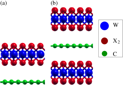
The systems under consideration are illustrated in Fig. 1. The lattice parameters of the graphene (9.98 Å) and WS2 supercells (9.57 Å) give rise to a lattice mismatch of 2.7%. The distance between the two subsystems converges to Å, see Table I, which is a typical value for graphene on a semiconducting substrate. We observe no modification of the CC bond lengths, whereas the WS bond lengths (2.45 Å to 2.46 Å) are modified as compared to pristine WS2 (2.39 Å yun ) because of the lattice mismatch. We find Å for graphene on WSe2 with a CC bond length of 1.42 Å, which is the value of pristine graphene. The WSe bond length (2.52 Å to 2.53 Å) is almost the same as in pristine WSe2 (2.52 Å yun ). Moreover, we obtain Å and Å for graphene sandwiched between WS2 and WSe2 layers, respectively, whereas the other structural parameters are the same as for the simple contacts.
Graphene is zero-gap semiconductor with very weak SOC Taroni . On the other hand, WS2 is semiconductor with a direct band gap of 1.30-1.35 eV Braga . Its structural and electronic properties have been studied extensively, see Ref. Huang and the references therein. WS2 is widely utilized for /-doped field effect transistors, for example Matthaus . Experimentally, the synthesis and characterization of graphene on WS2 has been reported in Ref. Georgiou . The authors claim that a device based on this system can operate at room temperature with good current modulating capacity. We show in Fig. 2(a) the band structure obtained for graphene on WS2 without SOC, demonstrating some interaction between the two subsystems, though without chemical bonding. The binding energy
where , , and are the total energies of the hybrid structure, WS2, and graphene, respectively, amounts to 53 meV per C atom, in agreement with Ref. Zhang . Due to this weak interaction, a small band gap of 0.9 meV is obtained, see the zoomed view in Fig. 2(a), with degeneracy of the K and K′ points.
When the SOC is switched on in the calculation, the spin degeneracy of the bands is lifted, resulting in valence and conduction band splittings of 33 meV, see Table I, with a small band gap of 0.7 meV, see the right hand side of Fig. 2(a). A similar behavior has been observed for graphene on Bi2Te3 and MoTe2 arxiv . The characteristic shape of the bands near the Fermi level signifies a QSH phase (band inversion under preserved time-reversal symmetry), similar to the observations in InAs/GaSb prl8 . It should be noted that the bands above and below the Fermi level have opposite spin in agreement with the signature of the QSH phase. A similar picture appears in germanene nanorods embedded in fully H-passivated germanene Seixas and in two-dimensional Sn Duan , for which the gap can be strongly enhanced by the application of the strain such that devices can operate at room temperature.
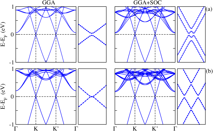
In Fig. 2(b) we present results for graphene sandwiched between WS2 layers. We find a 0.1 meV band gap without SOC and one of 1.1 meV when the SOC is taken into account. The shape of the band structure again reflects a QSH state. Larger valence and conduction band splittings of 92 meV and 99 meV, respectively, are achieved because two WS2 layers are attached to the graphene, see Table 1, similar to the 70 meV band splitting of graphene in contact with the (111) surface of BiFe3 (which is magnetic and thus hosts a quantum anomalous Hall effect prl14 ).
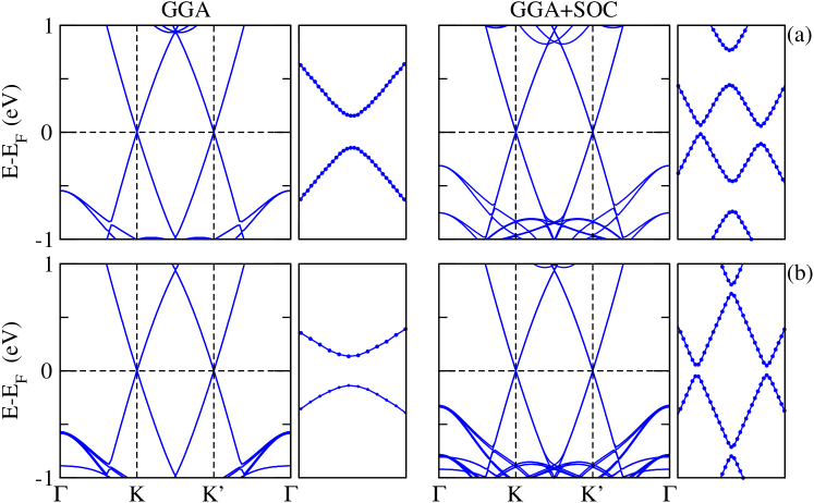
We also study hybrid systems with monolayer WSe2, which is a semiconductor with a band gap of 1.65 eV chang . The binding energy of graphene on WSe2 turns out to be 54 meV and thus is similar to the WS2 case. On the other hand, the band gap of 3.6 meV, see Fig. 3(a), is about 5 times larger than for WS2, reflecting the stronger SOC in WSe2. A comparison of the bulk properties of WS2 and WSe2 can be found in Refs. amin ; Rama , for example. Again, according to Fig. 3(a), the spin degeneracy at the K and K′ points is lifted under inclusion of the SOC. The band structure qualitatively reflects the same characteristics as demonstrated for WS2 in Fig. 2(a). However, the valence and conduction band splittings are enhanced to 145 meV and 132 meV, respectively, and so is the band gap (0.9 meV), see the zoomed view in Fig. 3(a). This finding is in agreement with the fact that the spin splitting due to SOC is about 50 meV larger in bulk WeS2 than in bulk WSe2 amin ; Rama . For graphene sandwiched between WSe2 layers, we find a reduction of the band gap from 3.0 meV to 1.0 meV under SOC with enhanced valence and conduction band splittings of 149 meV and 153 meV, respectively, compare Fig. 3(b) to Fig. 2(b), as to be expected from our previous discussion. In the WSe2 systems the QSH effect therefore is significantly more pronounced than in the WS2 systems.
IV Conclusion
Based on first-principles calculations, we have investigate the structural and electronic properties of hybrid systems consisting of graphene and WS or WSe2. Band gaps of few meV are obtained due to the interaction between the component materials. Moreover, band inversion is found at the K/K′ points, which indicates QSH states. By the preserved time-reversal symmetry together with the enhancement of the effective SOC in graphene, these systems are able to realize topological phases and therefore QSH states. Usually a strong magnetic field is needed to achieve a QSH state in graphene Young , while we propose systems in that a QSH state appears without magnetic field, which is a great advantage.
References
- (1) K. S. Novoselov, V. I. Fal’ko, L. Colombo, P. R. Gellert, M. G. Schwab, and K. Kim, Nature 490, 192 (2012).
- (2) A. K. Geim, Nature 499, 419 (2013).
- (3) S. Bertolazzi, D. Krasnozhon, and A. Kis, ACS Nano, 7, 3246 (2013).
- (4) T. Georgiou, R. Jalil, B. D. Belle, L. Britnell, R. V. Gorbachev, S. V. Morozov, Y.-J. Kim, A. Gholinia, S. J. Haigh, O. Makarovsky, L. Eaves, L. A. Ponomarenko, A. K. Geim, K. S. Novoselov, and A. Mishchenko, Nat. Nanotechnol. 8, 100 (2013).
- (5) B. A. Bernevig, T. L. Hughes, and S. C. Zhang, Science 314, 1757 (2006).
- (6) A. Roth, C. Brüne, H. Buhmann, L. W. Molenkamp, J. Mauciejko, X. L. Qi, and S. C. Zhang, Science 325, 294 (2009).
- (7) C. L. Kane and E. J. Mele, Phys. Rev. Lett. 95, 226801 (2005).
- (8) Y. Yao, F. Ye, X. L. Qi, S. C. Zhang, and Z. Fang, Phys. Rev. B 75, 041401 (2007).
- (9) C. Weeks, J. Hu, J. Alicea, M. Franz, and R. Wu, Phys. Rev. X 1, 021001 (2011).
- (10) J. Balakrishnan, G. K. W. Koon, M. Jaiswal, A. H. Castro Neto, and B. Özyilmaz, Nat. Phys. 9 284, (2013).
- (11) L. Kou, F. Hu, B. Yan, T. Wehling, C. Felser, T. Frauenheim, and C. Chen, arxiv:1309.6653v1.
- (12) A. F. Young, J. D. Sanchez-Yamagishi, B. Hunt, S. H. Choi, K. Watanabe, T. Taniguchi, R. C. Ashoori, and P. Jarillo-Herrero, Nature 505, 528 (2014).
- (13) W. Bao, Z. Zhao, H. Zhang, G. Liu, P. Kratz, L. Jing, J. Velasco, D. Smirnov, and C. N. Lau, Phys. Rev. Lett. 105, 246601 (2010).
- (14) P. Giannozzi, S. Baroni, N. Bonini, M. Calandra, R. Car, C. Cavazzoni, D. Ceresoli, G. L. Chiarotti, M. Cococcioni, I. Dabo, A. Dal Corso, S. de Gironcoli, S. Fabris, G. Fratesi, R. Gebauer, U. Gerstmann, C. Gougoussis, A. Kokalj, M. Lazzeri, L. Martin-Samos, N. Marzari, F. Mauri, R. Mazzarello, S. Paolini, A. Pasquarello, L. Paulatto, C. Sbraccia, S. Scandolo, G. Sclauzero, A. P. Seitsonen, A. Smogunov, P. Umari, and R. M. Wentzcovitch, J. Phys.: Condens. Matter 21, 395502 (2009).
- (15) G. Kresse and J. Furthmüller, Comput. Mater. Sci. 6, 15 (1996).
- (16) W. S. Yun, S. W. Han, S. C. Hong, I. G. Kim, and J. D. Lee, Phys. Rev. B 85, 033305 (2012).
- (17) A. Taroni, Nat. Mater. 12, 378 (2013).
- (18) D. Braga, I. G. Lezama, H. Berger, and A. F. Morpurgo, Nano Lett. 12, 5218 (2012).
- (19) W. Ki, X.-Y. Huang, J. Li, D. L. Young, and Y. Zhang, J. Mater. Res. 22, 1390 (2007).
- (20) A. Matthaus, A. Ennaoui, S. Fiechter, S. Tiefenbacher, T. Kiesewetter, K. Diesner, I. Sieber, W. Jaegermann, T. Tsirlina, and R. Tenne, J. Electrochem. Soc. 144, 1013 (1997).
- (21) S.-S. Li and C.-W. Zhang, J. Appl. Phys. 114, 183709 (2013).
- (22) C. Liu, T. L. Hughes, X.-L. Qi, K. Wang, and S.-C. Zhang, Phys. Rev. Lett. 100, 236601 (2008).
- (23) L. Seixas, J. E. Padilha, and A. Fazzio, Phys. Rev. B 89, 195403 (2014).
- (24) Y. Xu, B. Yan, H.-J. Zhang, J. Wang, G. Xu, P. Tang, W. Duan, and S.-C. Zhang, Phys. Rev. Lett. 111, 136804 (2013).
- (25) Z. Qiao, W. Ren, H. Chen, L. Bellaiche, Z. Zhang, A. H. MacDonald, and Q. Niu, Phys. Rev. Lett. 112, 116404 (2014).
- (26) C.-H. Chang, X. Fan, S.-H. Lin, and J.-L. Kuo, Phys. Rev. B 88, 195420 (2013).
- (27) A. Ramasubramaniam, Phys. Rev. B 86, 115409 (2012).
- (28) B. Amin, T. P. Kaloni, and U. Schwingenschlögl, RSC Adv. 4, 34561 (2014).