Conductance oscillations at the interface between a superconductor and the helical edge channel in a narrow HgTe quantum well.
Abstract
We experimentally investigate electron transport through the interface between a superconductor and the edge of a two-dimensional electron system with band inversion. The interface is realized as a tunnel NbN side contact to a narrow 8 nm HgTe quantum well. It demonstrates a typical Andreev behavior with finite conductance within the superconducting gap. Surprisingly, the conductance is modulated by a number of equally-spaced oscillations. The oscillations are present only within the superconducting gap and at lowest, below 1 K, temperatures. The oscillations disappear completely in magnetic fields, normal to the two-dimensional electron system plane. In contrast, the oscillations’ period is only weakly affected by the highest, up to 14 T, in-plane oriented magnetic fields. We interpret this behavior as the interference oscillations in a helical one-dimensional edge channel due to a proximity with a superconductor.
pacs:
73.40.Qv 71.30.+hRecently, a strong interest appears to the investigations of electron transport through the interface between a superconductor (S) and a normal (N) semiconductor-based low-dimensional structure. Because of the Majorana problem reviews , this interest is mostly connected with different SNS type structures, where the N region is a one-dimensional quantum wire Lutchyn ; Oreg ; Pientka ; Heiblum ; Mourik ; Deng or a topological surface state Fu ; yakoby .
An attractive example of a one-dimensional topological surface state is a current-carrying helical edge channel, realized in a narrow HgTe quantum well konig . This channel originates if the well thickness exceeds the critical 6.3 nm due to the inverted band structure in the bulk HgTe two-dimensional system pankratov ; zhang1 ; kane ; zhang2 . In contrast to the conventional quantum Hall edge states buttiker , this channel is helical, i.e. it consists of two spin-resolved counter-propagating states in zero magnetic field. Despite the initial idea of a topological protection konig ; zhang1 ; kane ; zhang2 , backscattering appears at macroscopic distances kvon ; kvon_nonlocal , possibly due to the allowed two-particle process mirlin and to the electron puddles glazman . The edge current has been directly demonstrated in a visualization experiment imaging in zero magnetic field. Also, the supercurrents have been investigated for a two-terminal SNS Josephson junction, with a rectangular section of quantum well located between two superconducting leads yakoby . So, a narrow HgTe quantum well is a promising candidate yakoby_top for the search for a topological superconductivity Sau1 ; Potter .
On the other hand, even a single SN interface is predicted to demonstrate a number of intriguing effects, e.g. conductance oscillations due to a proximity effect chevallier ; adroguer , giant spin rotation tanaka09 , and localized edge states guigou . Pronounced Fabry-Perot oscillations have been demonstrated for a three-dimensional topological insulator sandwiched between a superconducting and normal leads finck . In this experiment, a proximity with a superconductor doubled the period of the oscillations, although they were present also for normal leads. Thus, it seems to be reasonable to investigate electron transport in a single SN side contact at the edge of a narrow HgTe quantum well.
Here, we experimentally investigate electron transport through the interface between a superconductor and the edge of a two-dimensional electron system with band inversion. The interface is realized as a tunnel NbN side contact to a narrow 8 nm HgTe quantum well. It demonstrates a typical Andreev behavior with finite conductance within the superconducting gap. Surprisingly, the conductance is modulated by a number of equally-spaced oscillations. The oscillations are present only within the superconducting gap and at lowest, below 1 K, temperatures. The oscillations disappear completely in magnetic fields, normal to the two-dimensional electron system plane. In contrast, the oscillations’ period is only weakly affected by the highest, up to 14 T, in-plane oriented magnetic fields. We interpret this behavior as the predicted adroguer interference oscillations in a helical one-dimensional edge channel due to a proximity with a superconductor.
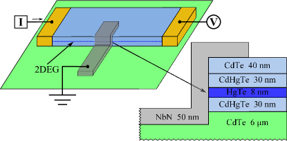
Our quantum well with [013] surface orientation and width nm is grown by molecular beam epitaxy. A detailed description of the well structure is given elsewhere growth1 ; growth2 . Because exceeds the critical value 6.3 nm, the quantum well is characterized by band inversion kvon ; kvon_nonlocal . It contains a two-dimensional electron gas (2DEG) with the electron density cm-2 and the low-temperature mobility cm2/Vs, as obtained from standard magnetoresistance measurements.
A sample sketch is presented in Fig. 1. A 200 nm high mesa step is formed by dry etching in Ar plasma. We fabricate two Ohmic contacts to the 2DEG by annealing In. In addition, we use dc magnetron sputtering to deposit a 50 nm thick superconducting NbN film at the mesa step, the surface is mildly cleaned by Ar plasma before sputtering. To avoid any 2DEG degradation, the sample is not heated during the sputtering process. The 20 m wide NbN stripe is formed by lift-off technique, with low (2-3 m) mesa overlap, see Fig. 1.
Because of the insulating layer on the top of the structure, a side SN junction is formed between the NbN electrode and the 2DEG edge at the mesa step. In samples with etched mesa an insulating region of finite width is always present at the 2DEG edge shklovskii ; image02 . In our samples this region is significant enough to provide tunnel S-2DEG junctions, which are characterized by M normal resistances .
We study electron transport across one particular NbN-2DEG junction in a three-point configuration: a current is applied between one of the In Ohmic contacts and a superconducting electrode which is grounded (see Fig. 1) while the other In contact measures the 2DEG potential. To obtain characteristics, we sweep the dc current through the interface from -4 nA to +4 nA. This dc current is modulated by a low ac (4 pA, 2 Hz) component. We measure both the dc () and ac () components of the 2DEG potential by using a dc voltmeter and a lock-in amplifier, respectively. The latter is equipped by a preamplifier with the 100 M input impedance. We have checked, that the lock-in signal is independent of the modulation frequency in the 1 Hz – 6 Hz range, which is defined by applied ac filters.
Because of the relatively low in-plane 2DEG resistance (about 1 k at present 2DEG concentration and mobility), and the low resistance of the superconducting NbN electrode, the measured curves reflect the behavior of the NbN-2DEG interface. To extract features specific to the HgTe edge transport, the measurements were performed at a temperature of 30 mK. Qualitatively similar results were obtained in several cooling cycles, for different absolute values of the junctions’ .
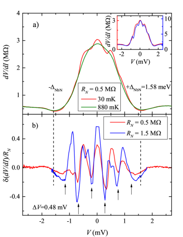
The examples of characteristics are presented in Fig. 2 (a). They demonstrate a behavior, which is qualitatively consistent with a standard Andreev one for a single SN junction tinkham . A clearly visible NbN superconducting gap can be determined 1.58 mV (denoted by dashed lines in Fig. 2), which corresponds well to the directly measured critical temperature K for a similar NbN film.
Within the gap at , the maximum differential resistance M is undoubtedly finite, which is only possible due to the Andreev reflection tinkham : if the Andreev process was suppressed, tunnel conductance would be zero at . According to the BTK theory tinkham , a single-particle scattering is significant at the SN interface, because exceeds the normal junction resistance value M. A corresponding transmission coefficient can be estimated tinkham as . Inset to Fig. 2 (a) demonstrates, that this ratio is the same for the junctions with strongly different .
On the other hand, the curves in the inset to Fig. 2 (a) are characterized by high values, 0.5 M and 1.5 M respectively. For a 20 m wide junction and cm-2 electron concentration, these correspond to the extremely low, below 10-3, junction transmission. This should result tinkham in a pure tunnel regime with zero conductance at . This is obviously not the case in Fig. 2 (a), so there is a clear contradiction between a well-developed Andreev behavior and high values.
Surprisingly, we also observe pronounced oscillations within the superconducting gap at for the lowest (30 mK) temperature, see Fig. 2 (a). The oscillating behavior is suppressed completely above 0.88 K, which is much below the critical K for our NbN film.
The conductance oscillations can be shown in detail by subtracting the high-temperature (0.88 K) monotonous curve from the low-temperature (30 mK) oscillating one. The result is shown in Fig. 2 (b) for the curves from the inset to Fig. 2 (a), i.e. for two junctions with strongly different (0.5 M and 1.5 M respectively). The positions of the oscillations are denoted by arrows in Fig. 2 (b). They coincide well and correspond to a constant period mV, while the oscillations’ visibility is evidently higher for the highest 1.5 M. The oscillations are concentrated strictly within the superconducting gap and demonstrate a resistance maximum at zero bias.
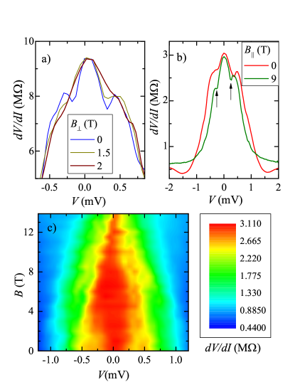
The observed conductance oscillations are sensitive to magnetic field. They disappear completely above the 2 T magnetic field, normal to the 2DEG plane, see Fig. 3 (a). In contrast, the oscillations survive well for the in-plane field configuration, see Fig. 3 (b). The monotonous evolution of the curve is shown in Fig. 3 (c). It can be seen that the NbN superconductivity is not suppressed, while the gap is obviously diminished at T. Above T, the oscillations’ period is also diminishing.
As a result, we observe (i) a well-developer Andreev behavior of curves for high M values; (ii) pronounced conductance oscillations at for the lowest (30 mK) temperature.
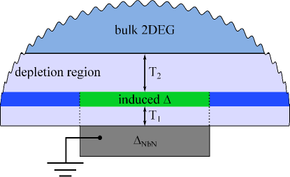
Let us start the discussion from the high-temperature curve in Fig. 2 (a). We observe a well-developed Andreev curve for high values of normal junction resistance . This contradiction can be removed, if there is a conductive channel inside the insulating region. In this case, is determined by the product , where the transmission corresponds to high coupling between this conductive channel and the NbN side contact, while this channel is weakly ( below 10-2) coupled to a bulk 2DEG, see Fig. 4.
The edge conductive channel is well known in narrow HgTe quantum wells as a current-carrying helical edge state konig , if the well thickness exceeds the critical 6.3 nm pankratov ; zhang1 ; kane ; zhang2 . The helical edge current has been demonstrated even to coexist with the conductive bulk by a direct visualization experiment imaging . This coexistence is also allowed by the theoretical considerations pankratov ; volkov , but requires a low coupling between the edge channel and the bulk. This is possible imaging in samples with etched mesa, where a depletion region of finite width is always present at the 2DEG edge, because of the smooth edge potential shklovskii ; image02 .
Thus, in a good accordance with previous investigations konig ; imaging , we can expect that a well-developed Andreev curve is determined by transport between the NbN side contact and the conductive helical edge channel. A corresponding value is mostly determined by the mismatch in Fermi velocities in NbN and the helical channel, and therefore is approximately the same for different junctions, as we can see from the perfect scaling of curves in the inset to Fig. 2 (a). In contrast, high values are mostly determined by low , which reflects a low transmission of a depletion region at the 2DEG edge. The latter is sensitive shklovskii ; image02 to the long-range fluctuations of the edge potential, i.e. is expected to be different for different junctions.
At low temperatures, we observe a number of equally spaced conductance oscillations. The oscillating behavior could be anticipated for a one-dimensional channel in a proximity with a superconductor due to either multiple Andreev reflections tinkham ; MAR or Andreev bound states formation chevallier . The former leads to resonances tinkham at , which are not equally spaced MAR . The latter produces equally-spaced modulation of the density of states chevallier , but requires a short contact , where is a coherence length, is a Fermi velocity, is a superconducting gap, induced in a one-dimensional channel.
The opposite limit of a long contact has been considered in Ref. adroguer, for a helical edge channel, realized in a narrow HgTe quantum well. Due to a proximity with NbN, a gap is opened in a one-dimensional channel, see Fig. 4. Thus, the channel is equivalent to a one-dimensional NSN structure in the vicinity of the NbN contact. Electrons with energies experience total local Andreev reflection at each SN interface, because of the helicity conservation adroguer . Electrons of very high energy are perfectly transmitted. For intermediate energies Bogoliubov quasiparticles experience Fabry-Perot-type transmission resonances within the superconductive region.
In our experiment, the conductive edge channel is coupled to the NbN side contact, so the resonances modulate the transmission . Thus, our experiment is somewhat equivalent to the described in Ref. finck, , where a three-dimensional topological insulator has been sandwiched between a superconducting and a normal lead, despite another limit in Ref. finck, , another dimension of a topological surface state, and different geometry of the experiment. The oscillations’ period can be estimated adroguer as . From the experimental period mV, contact width m, and we can estimate the Fermi velocity as , which is in a reasonable agreement with the calculated raichev . It’s worth noting, that Andreev bound states formation would require a similar expression for the oscillations’ period chevallier . However, we prefer the model of Ref. adroguer, , (i) because of the limit , and (ii) since the Andreev bound states should be primary seen in a coherent transport, i.e. in a supercurrent.
The conductance oscillations, therefore, are connected only with the electrons, which are approaching the NbN contact along the helical channel. A higher oscillations’ visibility for the highest 1.5 M in Fig. 2 (b) can be well understood: higher indicates higher decoupling of the helical channel from the bulk (i.e. lower ), which increases the number of electrons which are approaching the NbN contact along the channel. On the other hand, the oscillations’ period does not depend on , which is consistent with the experimental observation of a constant period mV for junctions with strongly different in Fig. 2 (b). The oscillations’ visibility is suppressed above , since the coupling to the NbN side contact is increased, see Fig. 2.
The proposed picture is also qualitatively consistent with the oscillations suppression at high temperatures and with the behavior in high magnetic fields. (i) The temperature smears the induced gap at 1 K, so a helical edge channel is normal in the vicinity of the NbN contact. This estimated temperature is consistent with the observed oscillations’ disappearance at K in our experiment. (ii) A normal magnetic field induces Landau quantization in a 2DEG. One-dimensional transport is also allowed in this case buttiker , so the Andreev behavior of the curve is not seriously changed in Fig. 3 (a). However, this edge transport is chiral buttiker , which forbids Fabry-Perot transmission resonance formation, proposed in Ref. adroguer, . In our samples, a well-developed Landau quantization appears in 2 T, which is consistent with the field of the oscillations’ disappearance. (iii) In-plane magnetic field does not destroy the edge channel helicity raichev . The superconducting gap is still resolved, see Fig. 3 (c), so the conductance oscillations survive in highest in-plane magnetic fields. According to the calculation raichev , is diminishing in high in-plane fields, which is also consistent with the observed diminishing of the oscillations’ period.
In conclusion, we experimentally investigate electron transport through the interface between a superconductor and the edge of a two-dimensional electron system with band inversion. The interface is realized as a tunnel NbN side contact to a narrow 8 nm HgTe quantum well. It demonstrates a typical Andreev behavior with finite conductance within the superconducting gap. Surprisingly, the conductance is modulated by a number of equally-spaced oscillations. The oscillations are present only within the superconducting gap and at lowest, below 1 K, temperatures. The oscillations disappear completely in magnetic fields, normal to the two-dimensional electron system plane. In contrast, the oscillations’ period is only weakly affected by the highest, up to 14 T, in-plane oriented magnetic fields. We interpret this behavior as the predicted adroguer interference oscillations in a helical one-dimensional edge channel due to a proximity with a superconductor.
We wish to thank A.M. Bobkov, I.V. Bobkova, Ya. Fominov, V.T. Dolgopolov, and T.M. Klapwijk for fruitful discussions. We gratefully acknowledge financial support by the RFBR (project No. 13-02-00065), RAS and the Ministry of Education and Science of the Russian Federation under Contract No. 14.B25.31.0007.
References
- (1) For recent reviews, see C. W. J. Beenakker, Annu. Rev. Con. Mat. Phys. 4, 113 (2013) and J. Alicea, Rep. Prog. Phys. 75, 076501 (2012).
- (2) R. M. Lutchyn, J. D. Sau, and S. D. Sarma, Phys. Rev. Lett. 105, 77001 (2010).
- (3) Y. Oreg, G. Refael, F. von Oppen, Phys. Rev. Lett. 105, 177002 (2010).
- (4) F. Pientka, G. Kells, A. Romito, P. W. Brouwer, and F. von Oppen, Phys. Rev. Lett. 109, 227006 (2012)
- (5) A. Das, Y. Ronen, Y. Most, Y. Oreg, M. Heiblum, and H. Shtrikman, Nature Physics 8, 887 (2012)
- (6) V. Mourik, K. Zuo, S. M. Frolov, S. R. Plissard, E. P. A. M. Bakkers, L. P. Kouwenhoven, Science 336, 1003 (2012).
- (7) M. T. Deng, C. L. Yu, G. Y. Huang, M. Larsson, P. Caroff, H. Q. Xu Nano Lett. 12, 6414 (2012).
- (8) L. Fu and C. L. Kane, Phys. Rev. Lett. 100, 96407 (2008).
- (9) Sean Hart, Hechen Ren, Timo Wagner, et.al., Nature Physics 10, 638–643 (2014)
- (10) M. König, S. Wiedmann, C. Brüne, A. Roth, H. Buhmann, L. W. Molenkamp, X.-L. Qi, and S.-C. Zhang, Science 318, 766 (2007).
- (11) B.A. Volkov and O.A. Pankratov, Pis’ma Zh. Eksp. Teor. Fiz. 42, 145 (1985) [JETP Lett. 42, 178 (1985)].
- (12) S. Murakami, N. Nagaosa, S.-C. Zhang, Phys. Rev. Lett. 93, 156804 (2004).
- (13) C. L. Kane, E. J. Mele, Phys. Rev. Lett. 95, 146802 (2005).
- (14) B. A. Bernevig, S.-C. Zhang, Phys. Rev. Lett. 96, 106802 (2006).
- (15) M. Büttiker, Phys. Rev. B 38, 9375 (1988).
- (16) G. M. Gusev, Z. D. Kvon, O. A. Shegai, еt al., PRB, 84, 121302(R) (2011).
- (17) G. M. Gusev, E. B. Olshanetsky, Z. D. Kvon, O. E. Raichev, N. N. Mikhailov, and S. A. Dvoretsky, Phys. Rev. B 88, 195305 (2013)
- (18) T.L. Schmidt, S. Rachel, F. von Oppen, and L.I. Glazman, Phys. Rev. Lett. 108, 156402 (2012); Nikolaos Kainaris, Igor V. Gornyi, Sam T. Carr, and Alexander D. Mirlin, Phys. Rev. B 90, 075118 (2014).
- (19) Jukka I. Vayrynen, Moshe Goldstein, and Leonid I. Glazman, Phys. Rev. Lett. 110, 216402 (2013); Jukka I. Vayrynen, Moshe Goldstein, Yuval Gefen, and Leonid I. Glazman, Phys. Rev. B 90, 115309 (2014)
- (20) K.C. Nowack, E.M. Spanton, M. Baenninger, et al., Nature Materials 12, 787 (2013).
- (21) S.-P. Lee, K. Michaeli, J. Alicea, and A. Yacoby, Phys. Rev. Lett. 113, 197001 (2014)
- (22) J. D. Sau, R. M. Lutchyn, S. Tewari, S. Das Sarma, Phys. Rev. Lett. 104, 040502 (2010).
- (23) A. C. Potter, P. A. Lee, Phys. Rev. Lett. 105, 227003 (2010).
- (24) D. Chevallier, P. Simon, and C. Bena, Phys. Rev. B 88, 165401 (2013).
- (25) P. Adroguer, C. Grenier, D. Carpentier, J. Cayssol, P. Degiovanni, and E. Orignac, Phys. Rev. B 82, 081303(R), (2010).
- (26) Takehito Yokoyama, Yukio Tanaka, and Naoto Nagaosa, Phys. Rev. Lett. 102, 166801 (2009).
- (27) M. Guigou, P. Rechter, J. Cayssol, and B. Trauzettel, Phys. Rev. B 84, 094534 (2011).
- (28) A.D.K. Finck, C. Kurter, Y.S. Hor, D.J. Van Harlingen, Phys. Rev. X 4, 041022 (2014)
- (29) Z. D. Kvon, E. B. Olshanetsky, D. A. Kozlov, N. N. Mikhailov, and S. A. Dvoretskii, Pis’ma Zh. Eksp. Teor. Fiz. 87, 588 (2008) [JETP Lett. 87, 502 (2008)].
- (30) E. B. Olshanetsky, Z. D. Kvon, N. N. Mikhailov, E. G. Novik, I. O. Parm, and S. A. Dvoretsky, Solid State Commun. 152, 265 (2012).
- (31) D. B. Chklovskii, B. I. Shklovskii, and L. I. Glazman, Phys. Rev. B 46, 4026 (1992).
- (32) E. Ahlswede, J. Weis, K. v. Klitzing, K. Eberl, Physica E, 12, 165 (2002).
- (33) G.E. Blonder, M. Tinkham, T.M. Klapwijk, Physical Review B, 25, 4515, (1982); M. Tinkham, Introduction to Superconductivity (2d ed., McGraw–Hill, New York, 1996).
- (34) V.V. Enaldiev, I.V. Zagorodnev, V.A. Volkov, arXiv:1407.0945
- (35) O. E. Raichev, Phys. Rev. B 85, 045310 (2012).
- (36) As a recent example, see H. Y. Günel, N. Borgwardt, I. E. Batov, et. al., Nano Lett., 14 (9), 4977 (2014).