Graphene optical-to-thermal converter
Abstract
Infrared plasmons in doped graphene nanostructures produce large optical absorption that can be used for narrow-band thermal light emission at tunable frequencies that strongly depend on the doping charge. By virtue of Kirchhoff’s law, thermal light emission is proportional to the absorption, thus resulting in narrow emission lines associated with the electrically controlled plasmons of heated graphene. Here we show that realistic designs of graphene plasmonic structures can release over 90% of the emission through individual infrared lines with 1% bandwidth. We examine anisotropic graphene structures in which efficient heating can be produced upon optical pumping tuned to a plasmonic absorption resonance situated in the blue region relative to the thermal emission. An incoherent thermal light converter is thus achieved. Our results open a radically different approach for designing tunable nanoscale infrared light sources.
The fabrication of intense, tunable infrared sources remains a challenge, despite the availability of quantum-cascade laser Faist et al. (1994), free-electron lasers Urata et al. (1998), and thermal emission bulbs. In particular, thermal emission has been extensively studied, leading to advances such as the control over its angular distribution from heated gratings Greffet et al. (2002) and fundamental insights on the coherence properties of the associated electromagnetic field near the emitting surfaces Carminati and Greffet (1999). Additionally, thermal emission has been shown, in combination with resonant metamaterial designs, to be confined within infrared peaks of high quality factor –the ratio of the energy width to the central energy of a peak– , which can be tuned by modifying the geometry Liu et al. (2011). Alternatively, fast electro-optical modulation can be achieved through the use of doped graphene, which has been demonstrated to display plasmons that are frequency-controlled via electrostatic gating Ju et al. (2011); Fei et al. (2011); Chen et al. (2012); Fei et al. (2012); Fang et al. (2013); Brar et al. (2013), reaching Fang et al. (2013). By conveniently shaping the graphene, it is possible to reach plasmon-mediated complete optical absorption over large areas Thongrattanasiri et al. (2012). Conversely, by virtue of Kirchhoff’s law, black-body light emission occurs in heated graphene at frequencies corresponding to the full-absorption resonances. Recently, conversion of broadband light to quasi-monochromatic emission has been achieved De Zoysa et al. (2012), while electrical modulation of the resulting emission has been successfully demonstrated Brar et al. . Electrical modulation of the emissivity has been also predicted using quantum wells Vassant et al. (2014) and recently demonstrated at 600 kHz Inoue et al. (2014).

Here, we explore the possibility of combining electrically modulated resonant thermal emission from graphene with light pumping in order to realize an optical converter. The conversion efficiency is strongly dependent on the strength of the plasmon resonances relative to the background. Using realistic parameters to describe the optical response of graphene, we predict that of the emission takes place within a single narrow plasmon line, with a net emission power W/m2 under realistic heating conditions (e.g., as estimated from a grey body with the absorptivity of Fig. 3(b) below, at a temperature K; incidentally, we use Gaussian units throughout this work). It should be noted that efficient narrow band emitter devices can be made based upon other types of optical resonators, such as for example plasmon nanocavities Ikeda et al. (2008), photonic crystals Lin et al. (2003); Chan et al. (2006); Inoue et al. (2013), metamaterials Liu et al. (2011), and semiconductors Streyer et al. (2013). However, graphene is unique in its combination of electrical tunability, which allows one to actively manipulate its absorption and thermal emission wavelengths at much higher modulation frequencies than other materials Inoue et al. (2014); low volume, which facilitates integration; and relatively low losses compared with other plasmonic materials.
We show in Fig. 1 a scheme of an optical-to-thermal converter. Graphene nanostructures are patterned on a thermally insulating dielectric membrane that is held in vacuum and mechanically sustained via narrow holding arms, so that thermal diffusion can be neglected and the main cooling mechanism of the graphene-substrate system is through radiative emission Brucoli et al. (2014). Heating can be introduced in different ways (e.g., Joule heating), but we concentrate here on optical pumping, realized at an absorption resonance frequency (e.g., tuned to a transverse-polarized plasmon of the graphene antennas depicted in Fig. 1). The graphene islands are chosen to have a high aspect ratio, so that emission is enhanced at a lower frequency associated with a plasmon polarized along the longitudinal direction (see below). In what follows, we assume the substrate to be poorly absorbing in the frequency range under consideration, and thus, we neglect it in our analysis of the radiation emission. The final efficiency of the system critically depends on this assumption, which requires the use of poorly absorbing materials.
From Kirchhoff’s law, the power emitted per unit frequency from a subwavelength structure at temperature held in vacuum is simply given by
| (1) |
where is the absorption cross-section for polarization along the principal direction (we neglect the response along the direction perpendicular to the graphene), is the power radiated by a blackbody per unit frequency and unit area, is the Bose-Einstein distribution, and the factor correctly accounts for the angle-integrated emission from a dipole. Before analyzing an extended surface (e.g., the device of Fig. 1), for which is simply the absorptivity times the area, we discuss the properties of an individual antenna.
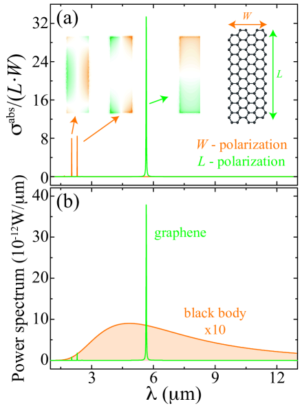
Figure 2(a) shows a characteristic absorption cross-section of a self-standing graphene rectangle nanoantenna of dimensions nmnm doped to a Fermi energy eV, for incoming light polarized along the width (W, orange line) or the length (L, green line) of the nanostructure. Although the cross section is several times larger than the geometrical area of the nanoantenna for both of these polarizations under the assumption of a realistic mobility Novoselov et al. (2004, 2005) cmV s, the longitudinal mode produces four times larger absorption than the transversal ones. Interestingly, this coincides with the length-to-width ratio of the rectangle, as expected from a spectral sum rule based upon the dipolar character of the modes García de Abajo (2014). The latter is confirmed by looking into the induced charge density maps [Fig. 2(a), insets]. The thermal emission from this antenna is shown in Fig. 2(b) at a temperature of 600 K (green curve), as obtained from Eq. (1). We emphasize that this emission is solely determined by the temperature and the absorption cross-section of the nanostructure. The high aspect ratio of the graphene island is important to have a large spectral separation between longitudinal and transversal modes, so that the former can then be placed closer to the blackbody emission maximum (orange curve), and thus, become the leading emission channel.
The three absorption resonances () observed in Fig. 2(a) are spectrally isolated, so that the island can be described through a polarizability near each of them (notice that the length is much smaller than the wavelength) with a Lorentzian profile García de Abajo (2014)
| (2) |
where is the graphene conductivity, whereas the coefficients and are only a function of the aspect ratio. More precisely, we find via finite-difference simulations (COMSOL) the values and for the transverse plasmons and for the longitudinal one. The effect of the substrate is included in this expression through its permittivity .
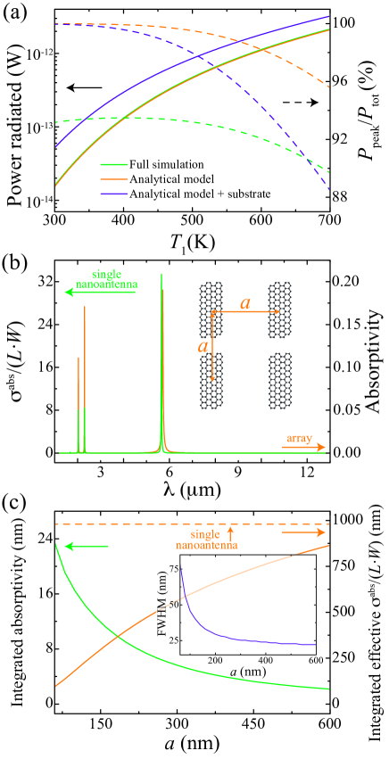
For simplicity, we analyze first the absorption/emission based on the cross section of isolated antennas, although the interaction between different sites in an array can produce some well-understood corrections García de Abajo (2014), as we discuss below. The absorption cross-section of a self-standing antenna reduces to under normal incidence. We use this expression to obtain the radiated power per antenna within each plasmon resonance of frequency as , assuming a Drude model for the conductivity , which also predicts . This analytical model produces nearly indistinguishable results when compared with the spectral integral of the absorption calculated with the local-RPA response. The temperature dependence, which is fully contained in the distribution function (see above), is analyzed in Fig. 3 using both models. Incidentally, the response also depends on temperature through the thermal smearing of the conduction electron band Falkovsky and Pershoguba (2007), although this is a small effect because we are in the regime. The emission increases with temperature, and interestingly, the fraction of emission within the longitudinal, long-wavelength mode stays at a high level up to temperatures above 700 K. The addition of a silica substrate (, included through Eq. (2) and also taking into account the modification in the emission near an interface Blanco and García de Abajo (2004)) only produces an overall increase in the emission, mainly towards the dielectric side [see Fig. 3(a)]. We should emphasize again that this high level of efficiency relies on the poor absorption of graphene over a wide spectral range determined by , so that practical implementations of this idea should fight any residual absorption in this material or in the substrate.
The interaction between antennas arranged in periodic arrays produces corrections in the emission efficiency, as well as moderate shifts in the emission peaks, as illustrated in Fig. 3(b), where we compare the absorption of a single antenna to simulations for extended antenna arrays using a dipole-based analytical model Thongrattanasiri et al. (2012), in which we calculate the array absorptivity averaged over polar angles and light polarizations for the two principal azimuthal directions. Although the maximum absorptivity of a plane wave by a self-standing array is Thongrattanasiri et al. (2012), averaging over polarizations and incidence directions limits this value to for an optimized separation between the antennas [period nm, see Fig. 3(c), left scale]. Also, the absorption efficiency per antenna decreases due to this interaction at relatively small separations [Fig. 3(b), right scale], although the integral of the main absorption peak over wavelengths yields a peak strength approaching the single island limit.
In conclusion, we have shown that electrically doped graphene can mediate the conversion of incident light into thermal radiation emitted at lower frequency via a suitable tailoring of the optical absorption profile. Our engineered structure allows achieving a concentration of the emission within a single narrow resonance. More efficient devices should be realizable upon optimization of geometrical and material parameters, with the constraint that the emitting elements have to be thermally isolated in order to prevent diffusive cooling. The electrical tunability of graphene can be used to change both the emission frequency Brar et al. and the absorption resonance. This could be achieved through a backgate that could simultaneously act as a mirror to reflect the backward emission. An interesting interplay takes place between the incident light power and the temperature reached by the structure before an equilibrium of the absorbed and emitted powers is achieved. A more efficient light extraction device could be designed by tunneling the graphene thermal emission through a resonant dielectric cavity placed in its vicinity, as suggested by a recent study of near-field radiative cooling Guha et al. (2012). This type of approach could also be exploited to guide the emission through a single output channel (e.g., a waveguide), in contrast to the broad angular emission distribution here studied. Our proposed concept of optical thermal conversion opens an unexplored approach towards the efficient generation of infrared light.
This work has been supported by the European Commission (Graphene Flagship CNECT-ICT-604391 and FP7-ICT-2013-613024-GRASP). A. M. acknowledges financial support from the Welch foundation through the J. Evans Attwell-Welch Postdoctoral Fellowship Program of the Smalley Institute of Rice University (Grant No. L-C-004).
References
- Faist et al. (1994) J. Faist, F. Capasso, D. L. Sivco, C. Sirtori, A. L. Hutchinson, and A. Y. Cho, Science 264, 553 (1994).
- Urata et al. (1998) J. Urata, M. Goldstein, M. F. Kimmitt, A. Naumov, C. Platt, and J. E. Walsh, Phys. Rev. Lett. 80, 516 (1998).
- Greffet et al. (2002) J. J. Greffet, R. Carminati, K. Joulain, J. P. Mulet, S. Mainguy, and Y. Chen, Nature 416, 61 (2002).
- Carminati and Greffet (1999) R. Carminati and J. J. Greffet, Phys. Rev. Lett. 82, 1660 (1999).
- Liu et al. (2011) X. Liu, T. Tyler, T. Starr, A. F. Starr, N. M. Jokerst, and W. J. Padilla, Phys. Rev. Lett. 107, 045901 (2011).
- Ju et al. (2011) L. Ju, B. Geng, J. Horng, C. Girit, M. Martin, Z. Hao, H. A. Bechtel, X. Liang, A. Zettl, Y. R. Shen, et al., Nat. Nanotech. 6, 630 (2011).
- Fei et al. (2011) Z. Fei, G. O. Andreev, W. Bao, L. M. Zhang, A. S. McLeod, C. Wang, M. K. Stewart, Z. Zhao, G. Dominguez, M. Thiemens, et al., Nano Lett. 11, 4701 (2011).
- Chen et al. (2012) J. Chen, M. Badioli, P. Alonso-González, S. Thongrattanasiri, F. Huth, J. Osmond, M. Spasenović, A. Centeno, A. Pesquera, P. Godignon, et al., Nature 487, 77 (2012).
- Fei et al. (2012) Z. Fei, A. S. Rodin, G. O. Andreev, W. Bao, A. S. McLeod, M. Wagner, L. M. Zhang, Z. Zhao, M. Thiemens, G. Dominguez, et al., Nature 487, 82 (2012).
- Fang et al. (2013) Z. Fang, S. Thongrattanasiri, A. Schlather, Z. Liu, L. Ma, Y. Wang, P. M. Ajayan, P. Nordlander, N. J. Halas, and F. J. García de Abajo, ACS Nano 7, 2388 (2013).
- Brar et al. (2013) V. W. Brar, M. S. Jang, M. Sherrott, J. J. Lopez, and H. A. Atwater, Nano lett. 13, 2541 (2013).
- Thongrattanasiri et al. (2012) S. Thongrattanasiri, F. H. L. Koppens, and F. J. García de Abajo, Phys. Rev. Lett. 108, 047401 (2012).
- De Zoysa et al. (2012) M. De Zoysa, T. Asano, K. Mochizuki, A. Oskooi, T. Inoue, and S. Noda, Nat. Photon. 6, 535 (2012).
- Brar et al. (0) V. W. Brar, M. C. Sherrott, L. A. Sweatlock, M. S. Jang, M. C. Laura Kim, and H. A. Atwater, arXiv 0, arXiv:1405.4145v1 (0).
- Ikeda et al. (2008) K. Ikeda, H. T. Miyazaki, T. Kasaya, K. Yamamoto, Y. Inoue, K. Fujimura, T. Kanakugi, M. Okada, K. Hatade, and S. Kitagawa, Appl. Phys. Lett. 92, 021117 (2008).
- Lin et al. (2003) S. Y. Lin, J. Moreno, and J. G. Fleming, Appl. Phys. Lett. 83, 380 (2003).
- Chan et al. (2006) D. L. C. Chan, M. Soljačić, and J. D. Joannopoulos, Opt. Express 14, 8785 (2006).
- Inoue et al. (2013) T. Inoue, M. D. Zoysa, T. Asano, and S. Noda, Appl. Phys. Lett. 102, 191110 (2013).
- Streyer et al. (2013) W. Streyer, S. Law, G. Rooney, T. Jacobs, and D. Wasserman, Opt. Express 21, 9113 (2013).
- Inoue et al. (2014) T. Inoue, M. De Zoysa, T. Asano, and S. Noda, Nat. Mater. 13, 928 (2014).
- Brucoli et al. (2014) G. Brucoli, P. Bouchon, R. Haïdar, M. Besbes, H. Benisty, and J.-J. Greffet, Appl. Phys. Lett. 105, 081101 (2014).
- Koppens et al. (2011) F. H. L. Koppens, D. E. Chang, and F. J. García de Abajo, Nano Lett. 11, 3370 (2011).
- Novoselov et al. (2004) K. S. Novoselov, A. K. Geim, S. V. Morozov, D. Jiang, Y. Zhang, S. V. Dubonos, I. V. Grigorieva, and A. A. Firsov, Science 306, 666 (2004).
- Novoselov et al. (2005) K. S. Novoselov, A. K. Geim, S. V. Morozov, D. Jiang, M. I. Katsnelson, I. V. Grigorieva, S. V. Dubonos, and A. A. Firsov, Nature 438, 197 (2005).
- García de Abajo (2014) F. J. García de Abajo, ACS Photon. 1, 135 (2014).
- Falkovsky and Pershoguba (2007) L. A. Falkovsky and S. S. Pershoguba, Phys. Rev. B 76, 153410 (2007).
- Blanco and García de Abajo (2004) L. A. Blanco and F. J. García de Abajo, Phys. Rev. B 69, 205414 (2004).
- Guha et al. (2012) B. Guha, C. R. Otey, C. B. Poitras, S. Fan, , and M. Lipson, Nano Lett. 12, 4546 (2012).
- Vassant et al. (2014) S. Vassant, I. Moldovan Doyen, F. Marquier, F. Pardo, U. Gennser, A. Cavanna, J. L. Pelouard, and J.-J. Greffet, Appl. Phys. Lett. 102, 081125 (2013).