Dimensionality-tuned electronic structure of nickelate superlattices explored by soft-x-ray angle resolved photoelectron spectroscopy
Abstract
The electronic and magnetic properties of epitaxial LaNiO3/LaAlO3 superlattices can be tuned by layer thickness and substrate-induced strain. Here, we report on direct measurements of the -space-resolved electronic structure of buried nickelate layers in superlattices under compressive strain by soft x-ray photoemission. After disentangling strong extrinsic contributions to the angle-dependent signal caused by photoelectron diffraction, we are able to extract Fermi surface information from our data. We find that with decreasing LaNiO3 thickness down to two unit cells (2 uc) quasiparticle coherence becomes strongly reduced, in accord with the dimension-induced metal-to-insulator transition seen in transport measurements. Nonetheless, on top of a strongly incoherent background a residual Fermi surface can be identified in the 2 uc superlattice whose nesting properties are consistent with the spin-density wave (SDW) instability recently reported. The overall behavior of the Ni spectra and the absence of a complete gap opening indicate that the SDW phase is dominated by strong order parameter fluctuations.
pacs:
79.60.-i, 79.60.Jv, 73.20.-r, 73.50.PzI Introduction
Artificial heterostructures made from transition metal oxides may host novel electronic and magnetic phases not present in the bulk of the constituents. Such phases may be controlled by, e.g., elastic strain or interfacial charge transfer.Hwang et al. (2012) In this context the perovskite LaNiO3 (LNO) is a very interesting material, as it is the only member of the NiO3 ( rare earth, viz., La, Pr, Nd, Sm, Eu) family showing metallic behavior with its partially-filled degenerate Ni ( and ) orbitals, while the other compounds exhibit a correlation-driven metal-insulator (MI) transition at low temperatures.Torrance et al. (1992); Imada et al. (1998) LNO is thus a highly correlated metal being close to an insulating phase, which may be switchable by interfacing.
Indeed, recent investigations have shown that the physical properties of LNO can be tuned by reducing its dimensionality or applying strain. For instance, density functional theory (DFT) calculations found that a single unit cell (uc) of LNO sandwiched between layers of the band insulator LaAlO3 (LAO) and thus under tensile strain displays a cuprate-like Fermi surface, identifying LNO as a possible candidate for exotic superconductivity.Chaloupka and Khaliullin (2008); Hansmann et al. (2009, 2010) Inspired by these predictions a large number of experimental and theoretical studies have been performed on ultra-thin films and superlattices (SLs). Scherwitzl et al. (2009, 2011); Sakai et al. (2013); Yoo et al. (2013); Benckiser et al. (2011); Boris et al. (2011); Chakhalian et al. (2011); Kaiser et al. (2011); Gray et al. (2011); Freeland et al. (2011); Frano et al. (2013); Wu et al. (2013); Han et al. (2011); Lee et al. (2011a, b)
Experimentally, ultra-thin films are found to exhibit a dimensional crossover from metallic to insulating behavior upon reducing the film thickness, with critical values ranging from 3 to 9 uc Scherwitzl et al. (2009, 2011); Sakai et al. (2013); Yoo et al. (2013). The situation is slightly different in LNO-based SLs: while thicker LNO layers embedded in SL structures remain metallic at all temperatures, 2 uc layers display a temperature-dependent MI transition.Boris et al. (2011) The critical temperature depends mainly on the epitaxial strain induced by the substrate. The strain also leads to a distortion of the octahedral ligand field and hence a lifting of the orbital degeneracy. The resulting orbital polarization increases almost linearly with the induced strain. Frano et al. (2013); Wu et al. (2013). The reason for the appearance of the insulating state in both SLs and ultra-thin films is still under debate. Different scenarios like Anderson localization, Scherwitzl et al. (2009, 2011) Mott insulator transition, Hansmann et al. (2009, 2010) charge disproportionation, Chakhalian et al. (2011); Liu et al. (2011) and spin density wave Boris et al. (2011); Frano et al. (2013) have been discussed.
It should be noted that in superlattices the necessity of octahedral connectivity across the interfaces in combination with strain induced by the substrate can stabilize different distortions compared to the situation in epitaxial films.Hwang et al. (2013); May et al. (2010) We emphasize in particular that in comparison to ultrathin films the superlattice structures allow for a better defined and efficient control of the strain effects. Since LNO with its LaO+ and NiO sublayers is polar, the (001)-oriented free surfaces of thin LNO films tend to reconstruct structurally by polar distortions or octahedral rotations to minimize the electrostatic energy. May et al. (2010, 2011); Kumah et al. (2014) The modified structure results in a change of the electronic structure, at least near the surface. In contrast, the LNO layers in the SLs are embedded in LAO, a host material of like polarity, and are thus stabilized against structural effects resulting from polar discontinuities, as shown by x-ray diffraction.Kumah et al. (2014)
Thus, the physical properties of the strained LNO layers and their dependence on dimensionality can be studied under clean conditions, i.e., in the absence of additional ionic or electronic surface and interface reconstructions
Direct insight into the electronic structure can be achieved by photoelectron spectroscopy (PES). Many of the scenarios mentioned above are reflected directly or indirectly in the microscopic electronic structure, i.e., in the single-particle spectral function, to which PES provides direct access. Such investigations have focused so far on (ultra-thin) films by angle-integrated Sakai et al. (2013) as well as angle-resolved PES (ARPES). Eguchi et al. (2009); Yoo et al. (2013); King et al. (2014) However, ARPES studies on SLs require a more bulk-sensitive approach, since the LNO layers are buried below several unit cells of the host material (LAO in our case). Conventional photoemission with low-energy photons is limited by its very low information depth of a few Angstroms only, determined by the photoelectron mean free path (MFP) and therefore cannot easily access the LNO layers. In contrast, photons in the soft x-ray (SX) regime allow for higher MFP at still reasonable momentum resolution (-resolution), thereby enabling -resolved probing of the buried electronic structure in such SLs.Berner et al. (2013a); Strocov et al. (2014)
In this study, we present SX-ARPES measurements on LNO/LAO SLs under compressive strain and a detailed analysis of the buried electronic structure. Besides a significant loss of quasiparticle (QP) coherence near the Fermi level () for the two-dimensional ground state, observed in the angle-integrated valence band spectra, our -resolved measurements trace the dimensional crossover from a three-dimensional Fermi surface in the 4 uc LNO-SL to two-dimensional behavior in the 2 uc LNO-SL. Although the intensity distribution in our -space maps is strongly affected by x-ray photoelectron diffraction (XPD), we are able to extract bandstructure information on the Ni -derived hole pocket states in all LNO/LAO SLs. An indication of the Ni -derived electron pocket is only observed in the 2 uc LNO-SL. The residual Fermi surface observed in this sample displays strong nesting properties which are consistent with the spin-density wave (SDW) scenario recently put forward as explanation for the insulating low-temperature ground state.
II Experiment
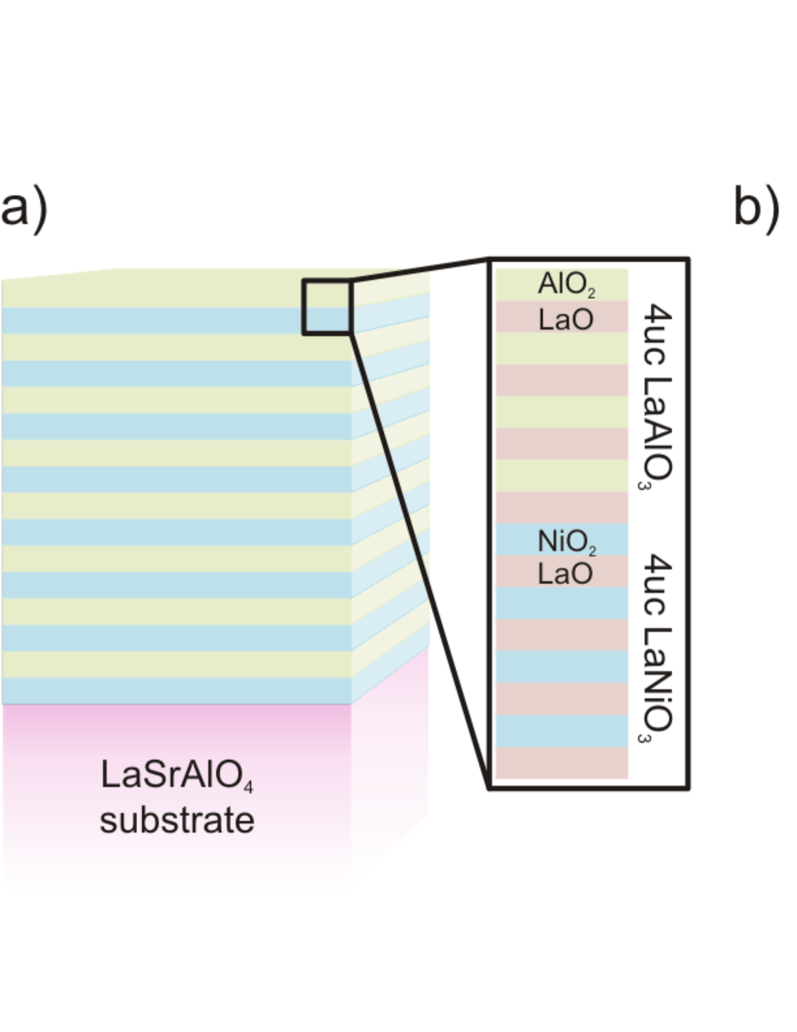
LNO/LAO superlattices with different LNO layer thickness were grown by pulsed laser deposition on (001) LaSrAlO4 (LSAO) single crystal substrates. The deposition starts with a number of (=2, 4) unit cells of LNO followed by the same number of LAO layers. This stacking sequence (//) is repeated fifteen and eight times for =2, 4, respectively, terminating with an LAO layer at the surface [see Fig. 1 (a)]. Additionally, a (10//4) SL was prepared being used as a thick LNO reference layer, also capped by 4 uc LAO.
The LNO/LAO stacks are compressively strained to the LSAO substrate, since the lattice mismatch between the LSAO and bulk pseudo-cubic LNO ( Å) García-Muñoz et al. (1992) is % (Ref. Wu et al., 2013). The induced biaxial strain, which is stable up to a SL thickness of nm (Ref. Frano et al., 2014), was confirmed by x-ray diffraction with lattice parameters Å and Å (Ref. Wu et al., 2013).
The photoemission experiments were performed at the ADRESS beamline of the Swiss Light Source with a SPECS Phoibos 150 spectrometer using -polarized photons.Strocov et al. (2010, 2014) The overall energy resolution was meV at a photon energy of 700 eV. During the experiment the samples were cooled down to K. Preliminary SX-ARPES experiments were performed at beamline BL25SU, SPring-8, Japan, to establish the feasibility of the method. Prior to the measurements the sample surface was cleaned by keeping the samples under ozone flow for 45 min, followed by an in situ annealing at 180∘C under mbar of oxygen for 45 min. This method was found to strongly suppress the amount of carbon-containing surface contaminants.
III Results
III.1 Angle integrated spectra
Figure 1 (b) shows the angle integrated valence band (VB) spectra of the (2//2), (4//4), and (10//4) SLs measured in normal emission geometry at low temperature ( K). Below eV the valence band mainly consists of superposed LAO and LNO O -derived states. Due to the valence band offset of eV between LAO and LNO (see Appendix A) the spectral weight between eV and can unambiguously be assigned to LNO states, in particular to the crystal-field split Ni and eg states at eV and at , respectively. The octahedral splitting is consistent with values observed in thin LNO films. Horiba et al. (2007); Gray et al. (2011); Sakai et al. (2013) The spectra are normalized to the same integrated area between eV and in order to facilitate easy identification of the changes in the Ni 3d states in this energy window. A normalization to the integral intensity of the full valence band (between eV and ) would not provide a meaningful comparison because of the superimposed LAO and LNO valence band contributions, whose relative intensities strongly change for different layer thicknesses due to the finite probing depth.
In the VB spectra of the (4//4) and (10//4) SL the derived feature shows a clear cut-off by the Fermi-Dirac-function at signalling that the samples remain metallic at low temperature down to a LNO layer thickness of 4 uc. This is consistent with electrical transport measurements shown in Fig. 1 (c) and recent results from optical ellipsometry on the same SLs. Boris et al. (2011)
In comparison, the VB spectrum of the (2//2) SL displays a remarkable change near the Fermi level: No Fermi edge can be identified, instead both the and features are smeared out indicating a loss of quasiparticle coherence. In contrast to a recent photoemission study of ultra-thin filmsSakai et al. (2013) our VB spectrum does not show a full band gap opening, but a distinct reduction of spectral weight at the Fermi level. Corresponding four point probe transport measurements of the identical samples confirm an insulating phase at low temperature and a temperature dependent MI crossover at K driven by the reduced dimensionality [see arrow in Fig. 1 (c)]. For very thin LNO layers such a transition has only been observed in SL structures, but not in films. Boris et al. (2011); Kumah et al. (2014)
III.2 -resolved spectra
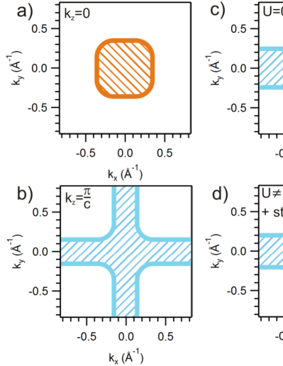
The angle-integrated spectra already demonstrate the pronounced effect of reduced LNO layer thickness on the electronic structure. In the following we study this in more detail by using the -space resolved spectra, in particular with respect to Fermi surface (FS) volume and topology. For the interpretation of the measured data it is helpful to start the discussion from the theoretical FS obtained by DFT calculations. Figure 2 shows cuts through the expected three-dimensional FS of bulk LNO parallel to the surface ( Å-1 and , denoting the wavevector component perpendicular to the surface) as well as the -independent two-dimensional FS of a single LNO layer (calculated without (c) and with (d) correlation effects), based on Refs. Hamada, 1993 and Hansmann et al., 2009, respectively. In the case of bulk LNO the Ni states form an electron pocket at the Brillouin zone (BZ) center ( point) [cf. Fig. 2 (a)], while the Ni orbitals create large hole pockets at the zone corners (A points) [cf. Fig. 2 (b)]. By reducing the LNO layer thickness, the three-dimensional FS transforms into a two-dimensional one, where both the electron and hole pockets are present [cf. Fig. 2 (c)]. Hansmann et al. showed that under tensile strain and influence of correlation effects the states can be lifted above the Fermi level and fully depopulated [cf. Fig. 2 (d)].
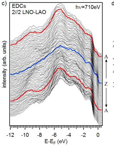
We begin our analysis of the -resolved data by investigating the spectra taken with a photon energy of 710 eV, which corresponds to a -space cut at (see Appendix B). Here the hole pockets should always be observable, independent of dimensionality or possible strain- or correlation-induced orbital polarization. Fig. 3 (a) and (c) show the energy distribution curves (EDCs) and (b) and (d) the corresponding momentum distribution curves (MDCs) of the (4//4) and (2//2) sample, respectively, along the A–Z–A direction of the BZ. Strongly dispersive O -derived bands are observed in both samples at lower energies between -8 to -10 eV, indicating the high-quality crystalline structure of our SLs. Furthermore, the periodic band dispersion allows a clear identification of the high symmetry points Z at Å-1 and A at . The superposition of LAO and LNO states between -8 and -2 eV hinders the detection of dispersions of the O -derived bands in this region. Near one can clearly identify the Ni states, although their intensity is much lower in comparison to the O -derived valence states.
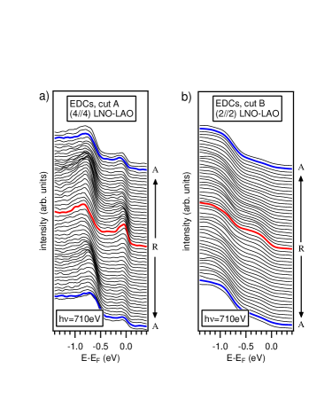
A more detailed view on the Ni states near the Fermi level is given in Fig. 4 (a) and (b), where the EDCs taken in A–R–A direction are shown for both samples. Interestingly, a large fraction of -independent intensity at the Fermi level is found. This loss of momentum information may be explained by non-direct transitions due to polaronic effects, as also reported for other oxide compounds. Dessau et al. (1998); Schrupp et al. (2005) Nevertheless, there is residual -dependent intensity modulation at the Fermi level in both samples (though of different strength), consistent with the expected Fermi level crossing of the band along A–R–A [cf. Fig. 2]. The EDCs of the (4//4) SL [see Fig. 4 (a)] exhibit an intense structure around R which can be assigned to the occupied states between the hole pockets. However, while Eguchi et al. found at this high-symmetry point a clearly dispersive band in their SX-ARPES study of a thick LNO film under comparable experimental conditionsEguchi et al. (2009), no dispersion is discernible in our measurement, already indicating a deviation of the SL from the bulk band structure.
In comparison to the (4//4) SL, where the Ni and states are well separated in energy, both features are considerably smeared out in the (2//2) SL [see Fig. 4 (b)]. Since the SL is well ordered as proven by the distinct dispersions in the O valence band, we attribute this behavior to the pronounced loss of QP coherence, as already discussed above. The reduced QP coherence furthermore prevents the identification of possible dispersive structures. An only very weak, but significant intensity modulation around the R point may be interpreted as a remnant of the occupied band states sitting on top of a largely -independent incoherent background.
III.3 X-ray photoelectron diffraction
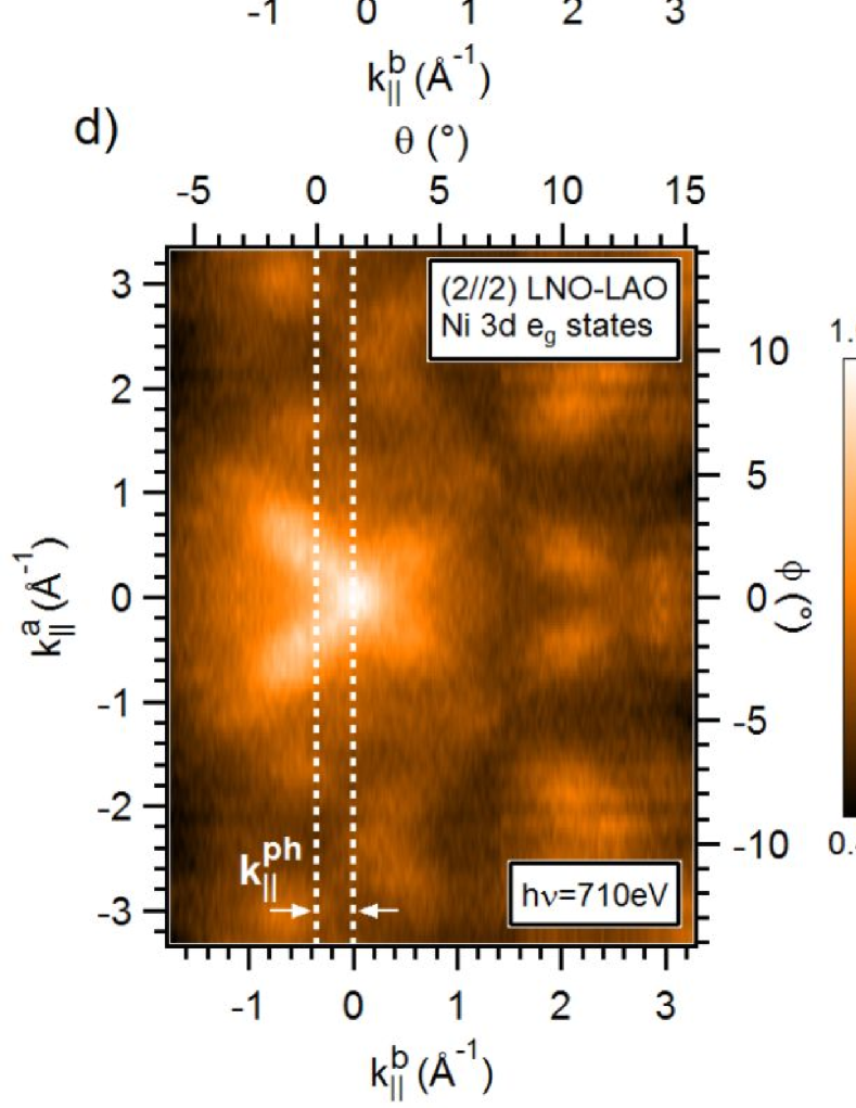
Figures 5 (a)–(e) show angle-resolved photoelectron distribution maps measured at different fixed binding energies (constant energy maps). The experimental geometry is sketched in Fig. 5 (f), where the angles and are rotation angles around the sample axes as indicated and describe the direction of photoelectron emission with respect to the surface normal.Strocov et al. (2014) By adjusting and a two-dimensional cut in momentum space, spanned by and , can be sampled (in our experiments the sample orientation was such that the and axes, defining the first Brillouin zone as in Fig. 2, were rotated by 45∘ with respect to and ). For the special case , the relation between the initial state momentum component parallel to the sample surface, , and is given by the following equation:
| (1) |
where is the free electron mass and the kinetic energy of the photoelectrons. denotes the parallel component of the photon momentum , which is transferred to the emitted photoelectron [see Fig. 5 (g)]. While this contribution can be neglected in low-energy ARPES measurements ( eV), it has to be taken into account in SX-ARPES when converting the angular scale to momentum scale. Note that in the given geometry a correction only for the -axis is sufficient, since the variation of is small and thus the lateral contribution of the photon momentum is negligible.
Figure 5 (a) and (b) show the constant energy maps of the (4//4) SL at the Fermi level ( states) and at eV ( states) integrated over energy windows of eV and eV, respectively. Note that only part of the full intensity range is captured by the color scale as is indicated for each map. Remarkable intensity modulations are observed in the map of the states. A more detailed analysis may be obtained from the angle-dependent measurements of the states in Fig. 5 (b): The chosen integration range corresponds roughly to the bandwidth of the fully occupied states, and hence the spectral weight distribution should simply reflect the momentum distribution function which for a completely occupied band is constant . However, strong intensity modulations are clearly observable exhibiting a geometric symmetry with respect to [cf. Fig. 5 (f)] but none with respect to any high-symmetry point or line in -space. This suggests that most of the intensity modulation may be attributed to x-ray photoelectron diffraction (XPD).Fadley (1990) Here, the excited photoelectron is viewed as a spherical wave originating at some emitting atom and elastically scattered off the neighboring atoms in the lattice. Interference results in an intensity pattern which is symmetric in the angle coordinates while modulations due to the electronic structure are symmetric in momentum space. Note that for the high kinetic energies used here forward scattering dominates the XPD process.Fadley (1987) The appearance of this effect in SX-ARPES measurements has been reported also for other oxide SL systems.Gray et al. (2013)
The angular intensity distribution of the photoemission map is additionally affected by the only partial -space occupation of the states, leading to the strongly reduced signal at small angles (with some remaining non-zero incoherent background). XPD effects are nonetheless well visible in the occupied part of the Brillouin zone, e.g., as pronounced intensity maxima at (such are seen also in the maps).
The identification of XPD as origin of the intensity modulations in the Ni states is supported by angle-resolved data of the Ni core level at eV [see Fig. 5 (c)]. The data were taken at a photon energy of eV in order to ensure the same kinetic energy, i.e., same wave length, as in the ARPES maps in Fig. 5 (a) and (b). The Ni XPD pattern — since core-levels are dispersionless, without intensity modulations owing to a momentum-dependence of the electronic structure — shows clear structure-induced symmetries about and and contains many of the features also seen in the Ni maps.
We observe similar intensity distributions in the angle-resolved maps of the - and states of the (2//2) SL, as shown in Fig. 5 (d) and (e), respectively. While the map of the fully occupied band again exhibits clear XPD-induced symmetry with respect to , the map of the states displays a superposition of -dependent state occupancy, e.g., the X-shaped structure at Å-1, and XPD-induced modulations, e.g., at .
The difference in the observed intensity modulations between both SLs at is explained on the one hand by the -dependent occupancy of the Ni states (see discussion in the next section). On the other hand the different layer thicknesses of LAO and LNO may lead to slightly different XPD modulation patterns, especially in the angle-resolved intensity distribution maps of the states.
III.4 Fermi surfaces
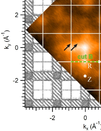
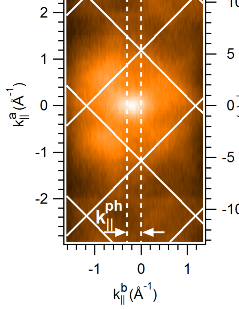
After having separated out the angular XPD effects in the photoemission maps taken at ( states) we now turn to the underlying -dependent structures resulting from the electronic structure, i.e., the Fermi surface of the buried LNO layers. For better identification we compare the measured intensity distributions, provided with a momentum scale, with the calculated Fermi surfaces in Fig. 6.
Starting with the (4//4) SL [Fig. 6 (a)], recorded at eV, which in the free-electron approximation for the final states corresponds to , we find qualitatively very good agreement with the calculated -space occupation at this very (gray shaded schematic). In particular, the hole pockets around the A points are clearly visible. As already discussed above, due to the moderate resolution of the experiment no sharp Fermi-level crossings of the dispersing bands can be observed. With the energy integration range ( eV) being comparable to the band width these maps essentially reflect the momentum distribution function , i.e., the occupied -space between the hole pockets rather than the FS contours [cf. shaded areas in Fig. 6 (a)].Straub et al. (1997)
The Fermi level intensity map of the (2//2) SL shown in Fig. 6 (b) basically resembles the expected momentum distribution function in the two-dimensional limit. Compared to the data of the (4//4) SL the structures are broader in -space. This can be explained by the change of the FS from the three-dimensional to the two-dimensional topology, where the hole pockets have to shrink in order to keep the Fermi volume constant [cf. Fig. 2], resulting in a broader occupied -space region between the hole pockets. At the Z point of the first BZ of the (2//2) SL some additional intensity is clearly visible, but much less so in higher-order zones, possibly due to matrix element effects. It is tempting to assign this intensity to the additional electron pocket in the center of the BZ predicted for the two-dimensional limit of Fig. 2 (c). That this intensity maximum is clearly centered around Å-1 (and not , see Fig. 5 (d)) supports the interpretation as genuine part of the band structure and rules out an XPD effect.
Both maps are taken at . Since for a three-dimensional, i.e., bulk-like, FS the electron pocket should only be visible at the -points (corresponding to integer multiples of in direction within the extended zone scheme), as can be seen from the theoretical FS in Fig. 2, it is interesting to look at FS cuts containing a point. The next available -point requires a photon energy of eV (see Appendix B). The intensity distribution map of the (2//2) SL shown in Fig. 7 (a) indeed exhibits significant intensity at the point, which may be a result of overlapping intensity derived from the Ni states at and XPD-induced modulations at . The diffuse intensity distribution towards the BZ edge may be interpreted as residual spectral weight of the occupied states between the hole pockets, although the very low Fermi level intensity prevents a more detailed analysis. In any case, the ubiquity of the zone center intensity for all photon energies (and thus its -independence) strongly supports the two-dimensional character of the FS in the (2//2) SL.
Figure 7 (b) shows the Fermi surface maps taken on the (4//4) SL at eV. Due to the thicker LNO layer one would expect to slowly recover bulk behavior with a stronger electron pocket signal at the point. However, we found no evidence for a -dependent state occupancy in our data. Rather, all intensity modulations exhibit a symmetry with respect to , identifying them as XPD-induced structures. To verify this result, we additionally performed angle-resolved measurements on the (10//4) SL at the same photon energy, since at 10 uc LNO layer thickness a closer approach to a fully established three-dimensional FS can be expected.Yoo et al. (2013) However, also in this SL no significant -dependent structures are detected, in particular, no electron pocket is found at the point [see Fig. 7 (c)]. Furthermore, a -space scan in direction by varying the photon energy from 580 to 820 eV (not shown here) did not reveal any signal which could be assigned to the Ni pocket around Å-1.
IV Discussion
The SX-ARPES data taken for ( eV) provide direct spectroscopic evidence of the predicted Ni -derived hole pockets in all investigated SL. However, for the electron pocket formed by Ni states in the BZ center indications are only found in the (2//2) SL. The angle-resolved data of both the (4//4) SL and (10//4) SL taken in the central plane of the BZ ( Å-1, i.e. eV) are strongly affected by XPD-induced intensity modulations and display no clear -dependent state occupancy. This is a surprising result, because a recent SX-ARPES study on thick LNO films has reported clear evidence of the Ni states and their three-dimensional dispersion.Eguchi et al. (2009)
It may be tempting to attribute this difference between confined LNO layers in SLs and bulk LNO to the strain induced by the substrate. However, a recent resonant reflectometry study focussing on the correlation between strain and orbital polarization in LNO/LAO SLs provides evidence that compressive strain enhances the Ni bandfilling compared to the situation in unstrained LNO.Benckiser et al. (2011); Wu et al. (2013) Conversely, tensile strain energetically lifts the orbital and causes its depopulation. This trend is supported by DFT calculations for ultra-thin LNO filmsMoon et al. (2012) and superlattices.Hansmann et al. (2009, 2010); Han et al. (2010); Blanca-Romero and Pentcheva (2011) Thus, the scenario that compressive strain induced by the LSAO substrate possibly leads to a strongly reduced Ni occupancy in our samples can most likely be excluded.
Another explanation is a much stronger XPD effect in the SL samples compared to bare LNO films. The data of both the (4//4)-SL and the (10//4) SL in Fig. 7 (b) and (c), respectively, show nearly identical intensity patterns, despite their different LNO layer thickness. They share however the same thickness of the LAO capping layer, and therefore it seems likely that most of the detected intensity modulations are caused by photoelectron diffraction within that layer. In SX-ARPES of bulk LNO films most of the Ni signal will originate from the top surface layers, whereas in LAO-capped SLs the photoelectron wave excited from the buried LNO layers will have to pass through the LAO overlayer and thus be subject to additional scattering and interference effects. The stronger XPD intensity modulations may then distort or even obscure any underlying -dependent bandstructure information. A test of this hypothesis would require a more systematic study of SL samples with varying LAO capping layer thickness.
A very clear and unambiguous result of our SX-ARPES study is the change in the microscopic electronic structure from the (4//4) SL to the (2//2) SL, indicating a significant loss of QP coherence concomitant with the dimension-controlled MI-crossover observed in transport. Different mechanisms have been proposed to explain the latter. For ultra-thin LNO films 2D Anderson localization has been discussed Scherwitzl et al. (2011), while other studies performed on ultra-thin filmsChakhalian et al. (2011) and SLs Liu et al. (2011), both under tensile strain, attribute the insulating phase to charge disproportionation in the two-dimensional ground state. Recent theoretical studies found strong evidence for a magnetic instability, i.e. the formation of a spin density wave (SDW), driven by FS nesting, with a wave vector as determined from the theoretical susceptibility.Lee et al. (2011a, b) This scenario is supported by spectroscopic data on PrNiO3-PrAlO3 superlattices.Hep Experimentally, muon-spin-rotation Boris et al. (2011) and resonant x-ray diffraction experiments Frano et al. (2013) indeed observed antiferromagnetic ordering at the predicted wavevector, but only in the (2//2) SL, independent of the used substrate, i.e., the induced strain. SLs with thicker LNO layers exhibit paramagnetic behavior, indicating that the SDW is closely linked to the reduced dimensionality.
Our measured spectroscopic data, especially on the FS topology, provide further support for the SDW scenario. Despite the pronounced loss of coherent quasiparticle weight in the (2//2) SL, the residual intensity modulation in the momentum distribution function reproduces a nearly quadratic shape of the FS hole pockets, with flat contours providing a good basis for strong FS nesting. Within experimental resolution the wavevector predicted for the ideal two-dimensional case () is indeed compatible with nesting of the experimental FS [see arrows in Fig. 6 (b)]. On the other hand, it may seem surprising that FS signal can still be observed in our low-temperature data, i.e. well within the SDW phase, because a nesting instability would normally open a gap and destroy the FS. However, as already seen in the EDCs of the (2//2) SL, there is no full gap opening at , at least within our experimental resolution. This behavior could be attributed to an insufficient SDW stabilization due to pronounced order parameter fluctuations, not fully unexpected in the two-dimensional limit. This picture is supported by very recent magneto-resistivity measurements performed on similar LNO/LAO SLs.Kumah et al. (2014) Hepting et al.Hep also find that the SDW state remains metallic, i.e. the gap does not encompass the entire FS. Order parameter fluctuations may also explain the suppression of quasiparticle coherence and the absence of SDW-induced band backfolding, in remarkable contrast to recent ARPES results on ultra-thin films. Yoo et al. (2013)
V Conclusions
In summary, we have investigated the electronic structure of compressively strained LNO/LAO SLs grown on LSAO substrates by angle-resolved soft x-ray photoemission. -integrated valence band spectra show a loss of quasiparticle coherence below 3 uc LNO layer thickness. Corresponding transport measurements exhibit a temperature dependent MI crossover in the (2//2) SL, while the (4//4) and (10//4) SLs stay metallic down to low temperatures.
Although the analysis of the angle-resolved measurements is complicated by strong XPD-induced intensity modulations, the measured angle-resolved maps reveal a dimensional crossover of the FS from three-dimensional in the (4//4) SL to two-dimensional behavior in the (2//2) SL. By comparing the maps with results from DFT calculations, the Ni states, which form the hole states around the A points, are clearly identified in the FS of all measured SLs. Evidence for the electron pocket derived from Ni orbital is found only in the (2//2) SL, but could not be observed for SLs with thicker LNO and LAO layers. We attribute this to pronounced XPD effects in the LAO overlayer, which interfere with or even obscure -dependent Fermi surface information
The measured FS topology, in particular the shape of hole pockets in the (2//2) SL, support FS nesting. This is consistent with the scenario of a dimensionality-induced SDW-instability, with the nesting properties of our experimental FS in excellent agreement with the reported SDW wavevector. Thus, our results strongly support magnetic ordering in the two-dimensional ground state of ultra-thin LNO layers embedded in a SL. In line with other experimental as well as theoretical studies, no indication of correlation-induced FS modifications was found for the SLs under compressive strain. Further studies, particularly on LNO/LAO SLs under tensile strain, are needed to investigate the tuneability of the electronic structure by strain and correlation effects in the two-dimensional limit.
Appendix A Valence band offset of the LaAlO3 overlayer
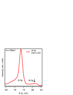
In the SLs the LNO layer is buried below a LAO capping layer. Thus, the measured valence band is a superposition of the LAO and LNO valence states. Only, if the valence band maximum of the insulating LAO, , is far enough below the Fermi level , the observed spectral weight near can unambiguously be assigned to the Ni states in the LNO layers. is determined by analyzing the position of a suitable core level from LAO, , Al , and comparing its position with a reference system containing LAO, where core-level position and valence band onset are well known. Here, we use as reference the well-studied LaAlO3/SrTiO3 heterostructure with eV and eV (Ref. Berner et al., 2013b). The energy position of the Al core level in the LNO/LAO SLs is found to be eV [see Fig. 8], independent of the LAO and LNO layer thickness. From the obvious relationship
| (2) |
we determine the position of the valence band maximum in the LAO overlayer as eV. Consequently, any spectral weight measured between and eV can only result from the Ni states in the LNO layers.
Appendix B -dependence for bulk LaNiO3
The relationship between the kinetic energy of the photoelectrons and the momentum perpendicular to the sample surface is described by the following equation including the non-negligible photon momentum component [see Fig. 5 (g)]:
| (3) |
where is the free electron mass, the inner potential, the kinetic energy, and the emission angle. For thick LNO films a value of eV has been reported.Eguchi et al. (2009) We do not expect a large variation of this phenomenological parameter for our LNO/LAO SLs. Thus, by using the lattice constant perpendicular to the surface Å (Ref. Wu et al., 2013) and taking the experimental geometry into account, the photon energies required for probing Fermi level states at the center ( Å-1) and the edge of the BZ () perpendicular to the surface are eV and eV, respectively.
Acknowledgements.
We thank C.S. Fadley and A.X. Gray for fruitful discussions. This work was supported by the Deutsche Forschungsgemeinschaft (FOR 1162) and the German Federal Ministry for Education and Research (05K10WW1).References
- Hwang et al. (2012) H. Y. Hwang, Y. Iwasa, M. Kawasaki, B. Keimer, N. Nagaosa, and Y. Tokura, Nature Mater. 11, 103 (2012).
- Torrance et al. (1992) J. B. Torrance, P. Lacorre, A. I. Nazzal, E. J. Ansaldo, and C. Niedermayer, Phys. Rev. B 45, 8209 (1992).
- Imada et al. (1998) M. Imada, A. Fujimori, and Y. Tokura, Rev. Mod. Phys. 70, 1039 (1998).
- Chaloupka and Khaliullin (2008) J. Chaloupka and G. Khaliullin, Phys. Rev. Lett. 100, 016404 (2008).
- Hansmann et al. (2009) P. Hansmann, X. Yang, A. Toschi, G. Khaliullin, O. K. Andersen, and K. Held, Phys. Rev. Lett. 103, 016401 (2009).
- Hansmann et al. (2010) P. Hansmann, A. Toschi, X. Yang, O. K. Andersen, and K. Held, Phys. Rev. B 82, 235123 (2010).
- Scherwitzl et al. (2009) R. Scherwitzl, P. Zubko, C. Lichtensteiger, and J.-M. Triscone, Appl. Phys. Lett. 95, 222114 (2009).
- Scherwitzl et al. (2011) R. Scherwitzl, S. Gariglio, M. Gabay, P. Zubko, M. Gibert, and J.-M. Triscone, Phys. Rev. Lett. 106, 246403 (2011).
- Sakai et al. (2013) E. Sakai, M. Tamamitsu, K. Yoshimatsu, S. Okamoto, K. Horiba, M. Oshima, and H. Kumigashira, Phys. Rev. B 87, 075132 (2013).
- Yoo et al. (2013) H. K. Yoo, S. Ill Hyun, L. Moreschini, Y. J. Chang, D. W. Jeong, C. H. Sohn, Y. S. Kim, H.-D. Kim, A. Bostwick, E. Rotenberg, J. H. Shim, and T. W. Noh, ArXiv e-prints (2013), arXiv:1309.0710 [cond-mat.str-el] .
- Benckiser et al. (2011) E. Benckiser, M. W. Haverkort, S. Brück, E. Goering, S. Macke, A. Frañó, X. Yang, O. K. Andersen, G. Cristiani, H.-U. Habermeier, A. V. Boris, I. Zegkinoglou, P. Wochner, H.-J. Kim, V. Hinkov, and B. Keimer, Nature Mater. 10, 189 (2011).
- Boris et al. (2011) A. V. Boris, Y. Matiks, E. Benckiser, A. Frano, P. Popovich, V. Hinkov, P. Wochner, M. Castro-Colin, E. Detemple, V. K. Malik, C. Bernhard, T. Prokscha, A. Suter, Z. Salman, E. Morenzoni, G. Cristiani, H.-U. Habermeier, and B. Keimer, Science 332, 937 (2011).
- Chakhalian et al. (2011) J. Chakhalian, J. M. Rondinelli, J. Liu, B. A. Gray, M. Kareev, E. J. Moon, N. Prasai, J. L. Cohn, M. Varela, I. C. Tung, M. J. Bedzyk, S. G. Altendorf, F. Strigari, B. Dabrowski, L. H. Tjeng, P. J. Ryan, and J. W. Freeland, Phys. Rev. Lett. 107, 116805 (2011).
- Kaiser et al. (2011) A. M. Kaiser, A. X. Gray, G. Conti, J. Son, A. Greer, A. Perona, A. Rattanachata, A. Y. Saw, A. Bostwick, S. Yang, S.-H. Yang, E. M. Gullikson, J. B. Kortright, S. Stemmer, and C. S. Fadley, Phys. Rev. Lett. 107, 116402 (2011).
- Gray et al. (2011) A. X. Gray, A. Janotti, J. Son, J. M. LeBeau, S. Ueda, Y. Yamashita, K. Kobayashi, A. M. Kaiser, R. Sutarto, H. Wadati, G. A. Sawatzky, C. G. Van de Walle, S. Stemmer, and C. S. Fadley, Phys. Rev. B 84, 075104 (2011).
- Freeland et al. (2011) J. W. Freeland, J. Liu, M. Kareev, B. Gray, J. W. Kim, P. Ryan, R. Pentcheva, and J. Chakhalian, Europhys. Lett. 96, 57004 (2011).
- Frano et al. (2013) A. Frano, E. Schierle, M. W. Haverkort, Y. Lu, M. Wu, S. Blanco-Canosa, U. Nwankwo, A. V. Boris, P. Wochner, G. Cristiani, H. U. Habermeier, G. Logvenov, V. Hinkov, E. Benckiser, E. Weschke, and B. Keimer, Phys. Rev. Lett. 111, 106804 (2013).
- Wu et al. (2013) M. Wu, E. Benckiser, M. W. Haverkort, A. Frano, Y. Lu, U. Nwankwo, S. Brück, P. Audehm, E. Goering, S. Macke, V. Hinkov, P. Wochner, G. Christiani, S. Heinze, G. Logvenov, H.-U. Habermeier, and B. Keimer, Phys. Rev. B 88, 125124 (2013).
- Han et al. (2011) M. J. Han, X. Wang, C. A. Marianetti, and A. J. Millis, Phys. Rev. Lett. 107, 206804 (2011).
- Lee et al. (2011a) S. B. Lee, R. Chen, and L. Balents, Phys. Rev. Lett. 106, 016405 (2011a).
- Lee et al. (2011b) S. B. Lee, R. Chen, and L. Balents, Phys. Rev. B 84, 165119 (2011b).
- Liu et al. (2011) J. Liu, S. Okamoto, M. van Veenendaal, M. Kareev, B. Gray, P. Ryan, J. W. Freeland, and J. Chakhalian, Phys. Rev. B 83, 161102 (2011).
- Hwang et al. (2013) J. Hwang, J. Son, J. Y. Zhang, A. Janotti, C. G. Van de Walle, and S. Stemmer, Phys. Rev. B 87, 060101 (2013).
- May et al. (2010) S. J. May, J.-W. Kim, J. M. Rondinelli, E. Karapetrova, N. A. Spaldin, A. Bhattacharya, and P. J. Ryan, Phys. Rev. B 82, 014110 (2010).
- May et al. (2011) S. J. May, C. R. Smith, J.-W. Kim, E. Karapetrova, A. Bhattacharya, and P. J. Ryan, Phys. Rev. B 83, 153411 (2011).
- Kumah et al. (2014) D. P. Kumah, A. S. Disa, J. H. Ngai, H. Chen, A. Malashevich, J. W. Reiner, S. Ismail-Beigi, F. J. Walker, and C. H. Ahn, Adv. Mat. 26, 1935 (2014).
- Eguchi et al. (2009) R. Eguchi, A. Chainani, M. Taguchi, M. Matsunami, Y. Ishida, K. Horiba, Y. Senba, H. Ohashi, and S. Shin, Phys. Rev. B 79, 115122 (2009).
- King et al. (2014) P. D. C. King, I. H. Wei, F. Y. Nie, M. Uchida, C. Adamo, S. Zhu, X. He, I. Bozovic, D. G. Schlom, and M. K. Shen, Nat. Nanotech. 9, 443 (2014).
- Berner et al. (2013a) G. Berner, M. Sing, H. Fujiwara, A. Yasui, Y. Saitoh, A. Yamasaki, Y. Nishitani, A. Sekiyama, N. Pavlenko, T. Kopp, C. Richter, J. Mannhart, S. Suga, and R. Claessen, Phys. Rev. Lett. 110, 247601 (2013a).
- Strocov et al. (2014) V. N. Strocov, X. Wang, M. Shi, M. Kobayashi, J. Krempasky, C. Hess, T. Schmitt, and L. Patthey, J. Synchrotron Rad. 21, 32 (2014).
- García-Muñoz et al. (1992) J. L. García-Muñoz, J. Rodríguez-Carvajal, P. Lacorre, and J. B. Torrance, Phys. Rev. B 46, 4414 (1992).
- Frano et al. (2014) A. Frano, E. Benckiser, Y. Lu, M. Wu, M. Castro-Colin, M. Reehuis, A. V. Boris, E. Detemple, W. Sigle, P. van Aken, G. Cristiani, G. Logvenov, H.-U. Habermeier, P. Wochner, B. Keimer, and V. Hinkov, Adv. Mat. 26, 258 (2014).
- Strocov et al. (2010) V. N. Strocov, T. Schmitt, U. Flechsig, T. Schmidt, A. Imhof, Q. Chen, J. Raabe, R. Betemps, D. Zimoch, J. Krempasky, X. Wang, M. Grioni, A. Piazzalunga, and L. Patthey, J. Synchrotron Rad. 17, 631 (2010).
- Horiba et al. (2007) K. Horiba, R. Eguchi, M. Taguchi, A. Chainani, A. Kikkawa, Y. Senba, H. Ohashi, and S. Shin, Phys. Rev. B 76, 155104 (2007).
- Hamada (1993) N. Hamada, J. Phys. Chem. Solids 54, 1157 (1993).
- Dessau et al. (1998) D. S. Dessau, T. Saitoh, C.-H. Park, Z.-X. Shen, P. Villella, N. Hamada, Y. Moritomo, and Y. Tokura, Phys. Rev. Lett. 81, 192 (1998).
- Schrupp et al. (2005) D. Schrupp, M. Sing, M. Tsunekawa, H. Fujiwara, S. Kasai, A. Sekiyama, S. Suga, T. Muro, V. A. M. Brabers, and R. Claessen, Europhys. Lett. 70, 789 (2005).
- Fadley (1990) C. S. Fadley, Synchrotron Radiation Research: Advances in Surface Science (Plenum, New York, 1990).
- Fadley (1987) C. S. Fadley, Physica Scripta 1987, 39 (1987).
- Gray et al. (2013) A. X. Gray, J. Minar, L. Plucinski, M. Huijben, A. Bostwick, E. Rotenberg, S.-H. Yang, J. Braun, A. Winkelmann, G. Conti, D. Eiteneer, A. Rattanachata, A. A. Greer, J. Ciston, C. Ophus, G. Rijnders, D. H. A. Blank, D. Doennig, R. Pentcheva, J. B. Kortright, C. M. Schneider, H. Ebert, and C. S. Fadley, Europhys. Lett. 104, 17004 (2013).
- Straub et al. (1997) T. Straub, R. Claessen, P. Steiner, S. Hüfner, V. Eyert, K. Friemelt, and E. Bucher, Phys. Rev. B 55, 13473 (1997).
- Moon et al. (2012) E. J. Moon, J. M. Rondinelli, N. Prasai, B. A. Gray, M. Kareev, J. Chakhalian, and J. L. Cohn, Phys. Rev. B 85, 121106 (2012).
- Han et al. (2010) M. J. Han, C. A. Marianetti, and A. J. Millis, Phys. Rev. B 82, 134408 (2010).
- Blanca-Romero and Pentcheva (2011) A. Blanca-Romero and R. Pentcheva, Phys. Rev. B 84, 195450 (2011).
- (45) Hepting et al., http://arxiv.org/abs/1410.8323 (Phys. Rev. Lett., in press).
- Berner et al. (2013b) G. Berner, A. Müller, F. Pfaff, J. Walde, C. Richter, J. Mannhart, S. Thiess, A. Gloskovskii, W. Drube, M. Sing, and R. Claessen, Phys. Rev. B 88, 115111 (2013b).