Defect in Phosphorene
Abstract
Defects are inevitably present in materials and always can affect their properties. Here, first-principles calculations are performed to systematically study the stability, structural and electronic properties of ten kinds of point defects in semiconducting phosphorene, including the Stone-Wales (SW-1 and SW-2) defect, single (SV59 and SV5566) and double vacancy (DV585-1, DV585-2, DV555777-1, DV555777-2, DV555777-3 and DV4104) defects. We find that these defects are all much easily created in phosphorene with higher areal density compared with graphene and silicene. They are easy distinguish each other and correlate with their defective atomic structures with simulated scanning tunneling microscopy images at positive bias. The SW, DV585-1, DV555777 and DV4104 defects have little effect on phosphorene’s electronic properties and defective phosphorene monolayers still show semiconducting with similar band gap values (about 0.9 ) to perfect phosphorene. The SV59 and DV585-2 defects can introduce unoccupied localized states into phosphorene’s fundamental band gap. Specifically, the SV59 and 5566 defects can induce hole doping in phosphorene, and only the stable SV59 defect can result in local magnetic moments in phosphorene different from all other defects.
pacs:
I Introduction
Two-dimensional (2D) ultrathin materials, such as graphene,NatureMater_6_183_2007 silicene,PRL_102_236804_2009 hexagonal boron nitride,NatureMater_3_404_2004 graphitic carbon nitrideNatureMater_8_76_2009 and molybdenum disulphide,NatureNanotechnol_6_147_2011 have received considerable interest recently owing to their outstanding properties and potential applications. Graphene,NatureMater_6_183_2007 a 2D sp2-hybridized carbon monolayer, is known to have remarkable electronic properties, such as a high carrier mobility, but the absence of a bandgap limits its applications of large-off current and high on-off ratio for graphene-based electronic devices. The same problem also exists in silicene, another well-known single silicon monolayer, which has most similar remarkable electronic properties to graphene but with buckled honeycomb structures.PRL_102_236804_2009
Most recently, a new 2D material, namely, phosphorene,PRB_86_035105_2012 ; JPCC_118_14051_2014 ; NatureNanotech_9_372_2014 ; NatureCommun_5_4475_2014 ; ACSNano_8_4033_2014 has been isolated in the experiments through mechanical exfoliation from bulk black phosphorus and has immediately received considerable attention. Phosphorene also shows some remarkable electronic properties superior to graphene and silicene. For example, phosphorene is a semiconductor with a direct bandgap of about 1 ,JPCC_118_14051_2014 showing the drain current modulation up to 105 and carrier mobility up to 103 cm2/(Vs) in nanoelectronics.NatureNanotech_9_372_2014 ; NatureCommun_5_4475_2014 ; ACSNano_8_4033_2014 Furthermore, up to now, besides graphene, phosphorene is the only stable elemental 2D material which can be mechanically exfoliated in the experiments.ACSNano_8_4033_2014 Therefore, introduced as an alternative to graphene,ScienceNews_185_13_2014 phosphorene may lead to faster semiconductor electronics in the future.
On the other hand, the properties of these 2D ultrathin materials are always affected by the presence of defects.ACR_2014 Typical point defects in graphene and silicene include Stone-Wales (SW) defect, single and double vacancy (SV and DV) defects.Nature_430_870_2004 ; NanoLett_7_2459_2007 ; ACSNano_5_26_2011 ; Nanoscale_5_9785_2013 ; PRB_88_045434_2013 Generally, both graphene and silicene have two kinds of SVs (SV59 and SV5566) and DVs (DV585 and DV555777), respectively. These defects are inevitably present in graphene and silicene and severely affect their structural and electronic properties,ACSNano_5_26_2011 ; Nanoscale_5_9785_2013 thus alter their applications.APL_93_193107_2008 ; Nanoscale_5_9062_2013 ; PCCP_15_5753_2013 However, up to now, little attention has been focused on the defects in phosphorene.NanoLett_14_6782_2014
In the present work, we systematically study the stability and electronic structures of typical point defects in semiconducting phosphorene using the density functional theory and ab-initio molecular dynamics calculations. We find that phosphorene has a wide variety of defects due to its low symmetry structure. Furthermore, these defects are all much easily created in phosphorene with regard to graphene and silicene and they are easy distinguish each other and correlate with their defective atomic structures with simulated scanning tunneling microscopy images at positive bias. Defects of different structures shows different stability and electronic structures in in phosphorene.
II Theoretical Methods and Models
First-principles calculations are based on the density functional theory (DFT) implemented in the VASP package.PRB_47_558_1993_VASP The generalized gradient approximation of Perdew, Burke, and Ernzerhof (GGA-PBE)PRL_77_3865_1996_PBE is chosen due to its good description of electronic structures of phosphorene,JPCC_118_14051_2014 grapheneACSNano_5_26_2011 and silicene.Nanoscale_5_9785_2013 All the geometry structures are fully relaxed until energy and forces are converged to 10-5 and 0.01 /Å, respectively. The energy cutoff is set to be 500 . The lattice parameters of phosphorene calculated to setup unit cell are (P) = 4.62 Å and (P) = 3.30 Å.JPCC_118_14051_2014 A large 5 7 supercell of phosphorene with a vacuum space about 15 Å in the Z direction is adopted to study the effect of various local defects in phosphorene. The surface Brillouin zone is sampled with a 3 3 regular mesh.
Ab-initio molecular dynamics (AIMD) simulations are employed to study the stability of defects in phosphorene. AIMD simulations are performed in a canonical ensemble. The simulations is performed during 2.0 with a time step of 2.0 at the temperature of 400 controlled by using the Nose-Hoover method.PRB_51_13705_1995_NoseHoover
III Results and Discussion
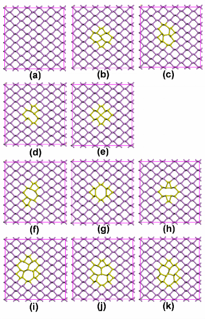
We first check the geometric properties of defects in phosphorene as shown in Figure 1. Typical point defects of SW, SV59, SV5566, DV585 and DV555777 in grapheneACSNano_5_26_2011 and siliceneNanoscale_5_9785_2013 also can be formed in phosphorene, but which has a wide variety of defects because of lower symmetry structure. There are two kinds of SW (SW-1 and SW-2) and DV585 (DV585-1 and DV585-2) defects respectively, three kinds of DV555777 (DV555777-1, DV555777-2 and DV555777-3) defects in phosphorene as shown in Figure 1. Interestingly, we find a new stable structure of DV defect in phosphorene, namely 4104, as shown in Figure 1(h), which has not been observed in both graphene and silicene.
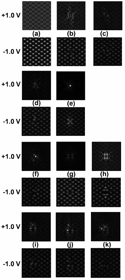
To help recognize the defects in future experiments, the scanning tunneling microscopy (STM) images of perfect and defective phosphorene are simulated at +1.0 and -1.0 bias as shown in Figure 2. At positive bias (+1.0 ), the STM images of these defects are easy to understand and correlate with their defective atomic structures. But at negative bias (-1.0 ), the STM images of perfect and defective phosphorene are difficult to distinguish each other due to a direct consequence of height variation for the buckling of phosphorene.
Then, we study the stability of defects in phosphorene. To characterize the stability of a defect in phosphorene, we define its formation energy as
where represents the total energy of defective phosphorene, is the energy per phosphorus atom in a perfect phosphorene sheet and corresponds to the number of phosphorus atoms in phosphorene. Notice that for perfect phosphorene, (Phosphorene) = 0 . Perfect phosphorene shows less stable with a smaller cohesive energy of 3.48 /atom compared with graphene (7.90 /atom) and silicene (3.96 /atom).Nanoscale_5_9785_2013 Our calculated stability of perfect and defective phosphorene, graphene and silicene are summarized in Table 1 and Table 2.
| Perfect | 0.000 | 0.000 | 0.905 |
| SW-1 | 1.012 | 0.003 | 0.928 |
| SW-2 | 1.322 | 0.003 | 0.883 |
| SV59 | 1.626 | 0.980 | 0.190/0.941 |
| SV5566 | 2.025 | 0.000 | Hole doping |
| DV585-1 | 1.906 | 0.002 | 0.962 |
| DV585-2 | 3.041 | 0.002 | 0.559 |
| DV4104 | 2.137 | 0.000 | 0.929 |
| DV555777-1 | 2.081 | 0.002 | 0.966 |
| DV555777-2 | 2.350 | 0.002 | 0.962 |
| DV555777-3 | 2.613 | 0.003 | 0.973 |
| Phosphorene | Graphene | Silicene | |
| Reference | This work | Ref.ACSNano_5_26_2011 | Ref.Nanoscale_5_9785_2013 |
| (Perfect) | 3.48 | 7.90 | 3.96 |
| (SW) | 1.011.32 | 4.50 | 2.09 |
| (SV59) | 1.63 | 7.80 | 3.77 |
| (SV5566) | 2.03 | 3.01 | |
| (DV585) | 1.913.04 | 7.52 | 3.70 |
| (DV555777) | 2.082.61 | 6.40 | 2.84 |
| (DV4104) | 2.13 |
We find that the SW-1 defect is most easily formed in phosphorene with the smallest formation energy of 1.01 among various defects similar to grapheneACSNano_5_26_2011 and silicene.Nanoscale_5_9785_2013 For DVs, the 585 and 555777 defects are also stable in phosphorene similar to graphene and silicene. Interestingly, we find the most stable DV in phosphorene is 4104 with a small formation energy of 2.13 , but which can not formed in graphene and silicene. Notice that defective phosphorene monolayers all have smaller formation energy compared with defective graphene and silicene with the same types of defects as summarized in Table 2.
To further study the thermal stability of perfect and defective phosphorene, AIMD simulations are performed at 400 . In the initial state ( = 0.0 ), perfect and defective phosphorene monolayers are set to optimized geometric structures. We find that the perfect phosphorene and most of phosphorene monolayers are stable at 400 during = 2.0 . The only unstable one is the SV5566 defect in phosphorene, which trends to change into more stable SV59 defect in phosphorene at 400 .
At finite temperature , defects’ areal density () in 2D materials follows the Arrhenius equation
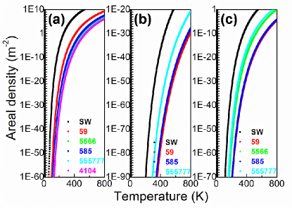
where is the areal density of atoms in perfect 2D materials, is the formation energy of a defect formed in materials and is the Boltzmann constant. For perfect phosphorene, graphene and silicene, their areal densities are (Phosphorene) = 2.62 , (Graphene) = 3.79 and (Silicene) = 1.55 , respectively. The temperature-dependence areal density of the most stable defects in phosphorene, graphene and silicene is calculated and plotted in Figure 3. The results show that these defects have much higher areal density and they are much easily created in phosphorene compared with graphene and silicene.
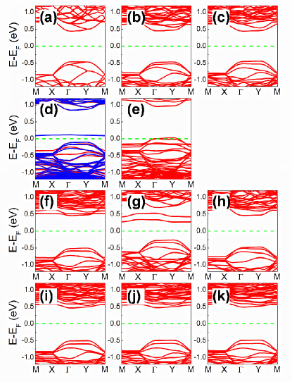
Finally, we check the electronic band structures of perfect and defective phosphorene as shown in Figure 4. Monolayer phosphorene is semiconducting with a direct band gap of 0.91 (Figure 4(a)), which agrees well with previous theoretical studies.JPCC_118_14051_2014 We find that the SV59 defect can induce local magnetic moments in phosphorene with a magnetic moment of 0.98 B, but other defective phosphorene monolayers are not magnetic similar to silicene.Nanoscale_5_9785_2013 Furthermore, the SW, DV555777 and DV4104 defects have little effect on phosphorene’s electronic properties, still showing semiconducting with similar band gap values (about 0.9 ) for defective phosphorene, different from grapheneACSNano_5_26_2011 and silicene.Nanoscale_5_9785_2013 Defective phosphorene with the DV585 defects are also semiconductors but with different band gaps (0.96 and 0.56 respectively for DV585-1 and DV585-2). The SV59 and DV585-2 defects can introduce unoccupied localized states into phosphorene’s fundamental band gap as shown in Figure 4(d) and (g). Specifically, the SV defects can induce hole doping in phosphorene as shown in Figure 4(d) and (e), which can increase the hole carrier concentration of semiconducting phosphorene. Notice that phosphorene has a high areal density for the SV defects, agreeing well with a high hole mobility observed in phosphorene in recent experiments.ACSNano_8_4033_2014
IV Conclusions
In summary, we systematically study the stability and electronic structures of defects in semiconducting phosphorene using the density functional theory and ab-initio molecular dynamics calculations. We find that phosphorene has a wide variety of point defects (SW-1, SW-2, SV59, SV5566, DV585-1, DV585-2, DV555777-1, DV555777-2, DV555777-3 and DV4104) due to its low symmetry structure. Furthermore, these defects are all much easily created in phosphorene with regard to graphene and silicene and they are easy distinguish each other and correlate with their defective atomic structures with simulated scanning tunneling microscopy images at positive bias. Defects of different structures shows different stability and electronic structures in in phosphorene. The SW, DV585-1, DV555777 and DV4104 defects have little effect on phosphorene’s electronic properties and defective phosphorene monolayers still show semiconducting with similar band gap values (about 0.9 ) to perfect phosphorene. The SV59 and DV585-2 defects can introduce unoccupied localized states into phosphorene’s fundamental band gap. Specifically, the SV59 and 5566 defects can induce hole doping in phosphorene, and only the stable SV59 defect can result in local magnetic moments in phosphorene different from all other defects. The present theoretical results provide valuable insights into the identification of defects in further experiments and the understanding their effects on the properties and applications of phosphorene.
V ACKNOWLEDGMENTS
This work is partially supported by the National Key Basic Research Program (2011CB921404), by NSFC (11404109, 21121003, 91021004, 21233007, 21222304), by CAS (XDB01020300). This work is also partially supported by the Scientific Discovery through Advanced Computing (SciDAC) program funded by U.S. Department of Energy, Office of Science, Advanced Scientific Computing Research and Basic Energy Sciences (W. H.). We thank the National Energy Research Scientific Computing (NERSC) center, USTCSCC, SC-CAS, Tianjin, and Shanghai Supercomputer Centers for the computational resources.
References
- (1) A. K. Geim and K. S. Novoselov, Nature Mater. 6, 183 (2007).
- (2) S. Cahangirov, M. Topsakal, E. Aktürk, H. Şahin, and S. Ciraci, Phys. Rev. Lett. 102, 236804 (2009).
- (3) K. Watanabe, T. Taniguchi, and H. Kanda, Nature Mater. 3, 404 (2004).
- (4) X. Wang, K. Maeda, A. Thomas, K. Takanabe, G. Xin, J. M. Carlsson, K. Domen, and M. Antonietti, Nature Mater. 8, 76 (2009).
- (5) B. Radisavljevic, A. Radenovic, J. Brivio, V. Giacometti, and A. Kis, Nature Nanotech. 6, 147 (2011).
- (6) S. Appalakondaiah, G. Vaitheeswaran, S. Leb gue, N. E. Christensen, and A. Svane, Phys. Rev. B 86, 035105 (2012).
- (7) H. Guo, N. Lu, J. Dai, X. Wu, and X. C. Zeng, J. Phys. Chem. C 118, 14051 (2014).
- (8) L. Li, Y. Yu, G. Ye, Q. Ge, X. Ou, H. Wu, D. Feng, X. Chen, and Y. Zhang, Nature Nanotech. 9, 372 (2014).
- (9) J. Qiao, X. Kong, Z.-X. Hu, F. Yang, and W. Ji, Nature Commun. 5, 4475 (2014).
- (10) H. Liu, A. T. Neal, Z. Zhu, Z. Luo, X. Xu, D. Tománek, and P. D. Ye, ACS Nano 8, 4033 (2014).
- (11) G. Andrew, Science News 185, 13 (2014).
- (12) X. Zou and B. I. Yakobson, Acc. Chem. Res. DOI: 10.1021/ar500302q (2014).
- (13) A. Hashimoto, K. Suenaga, A. Gloter, K. Urita, and S. Iijima, Nature 430, 870 (2004).
- (14) R. G. Amorim, A. Fazzio, A. Antonelli, F. D. Novaes, and A. J. R. da Silva, Nano Lett. 7, 2459 (2007).
- (15) F. Banhart, J. Kotakoski, and A. V. Krasheninnikov, ACS Nano 5, 26 (2011).
- (16) J. Gaoab, J. Zhang, H. Liu, Q. Zhang and J. Zhao, Nanoscale 5, 9785 (2013).
- (17) H. Sahin, J. Sivek, S. Li, B. Partoens, and F. M. Peeters, Phys. Rev. B 88, 045434 (2013).
- (18) O. Leenaerts, B. Partoens, and F. M. Peeters, Appl. Phys. Lett. 93, 193107 (2008).
- (19) W. Hu, X. Wu, Z. Li and J. Yang, Nanoscale 5, 9062 (2013).
- (20) W. Hu, X. Wu, Z. Li, and J. Yang, Phys. Chem. Chem. Phys. 15, 5753 (2013).
- (21) Y. Liu, F. Xu, Z. Zhang, E. S. Penev, and B. I. Yakobson, Nano Lett. 14, 6782 (2014).
- (22) G. Kresse and J. Hafner, Phys. Rev. B 47, 558 (1993).
- (23) J. P. Perdew, K. Burke, and M. Ernzerhof, Phys. Rev. Lett. 77, 3865 (1996).
- (24) S. N. Khanna and P. Jena, Phys. Rev. B 51, 13705 (1995).