Manipulating Andreev and Majorana Bound States with microwaves
Abstract
We study the interplay between Andreev (Majorana) bound states that form at the boundary of a (topological) superconductor and a train of microwave pulses. We find that the extra dynamical phase coming from the pulses can shift the phase of the Andreev reflection, resulting in the appearance of dynamical Andreev states. As an application we study the presence of the zero bias peak in the differential conductance of a normal-topological superconductor junction - the simplest, yet somehow ambiguous, experimental signature for Majorana states. Adding microwave radiation to the measuring electrodes acts as a probe of the Andreev nature of the zero bias peak.
Andreev bound states and their topological counterparts, Majorana states, have seen considerable renewed interest springing from the possibility of using the latter for topologically protected quantum computation Nayak et al. (2008). These Majorana states were first proposed to appear at the boundaries of so-called topological superconductors (TSs), rather exotic materials Kitaev (2001); Ivanov (2001); Fu and Kane (2008). Although the search for a “natural” TS is very active, another route consists of engineering a TS by putting a regular (s-wave) superconductor into contact with another material that has strong spin-orbit interaction. A quantum spin Hall (QSH) topological insulator in contact with a superconductor is a popular possibility Mi et al. (2013). Another promising proposal is to use a semiconducting nanowire in contact with a superconductor Lutchyn et al. (2010); Oreg et al. (2010). Indeed, a possible signature of the existence of Majorana states in a semi-conducting nanowire coupled to a superconducting electrode was recently reported Das et al. (2012); Mourik et al. (2012); Deng et al. (2012); Churchill et al. (2013).
In this letter we report on a dynamical generalization of Andreev/Majorana states in the presence of train of microwave pulses, i.e. the possibility to detect and manipulate these states by bringing the system out of equilibrium. Our proposal shares some features with other recent proposals that went under the name of “Floquet Majorana” states Jiang et al. (2011); Liu et al. (2012a, 2013); Kundu and Seradjeh (2013): zero energy bound states that can be stabilized by a finite frequency perturbation. Our mechanism is, however, rather different and uses a simpler perturbation (oscillating voltage) applied to an electrode (as opposed to the whole system) together with much smaller frequencies ( to ).
The dynamical Andreev states could be used to discriminate true Majoranas from other phenomena. Indeed, experimental evidence reported so far for Majorana states are based entirely on the presence (or lack) of a zero bias peak in the differential conductance. The peak could, however, originate from different sources Pikulin et al. (2012); Lee et al. (2012); Chang et al. (2013); Cheng et al. (2014); Žitko et al. (2015); Liu et al. (2012b); Lutchyn et al. (2011); Kells et al. (2012a); Lee et al. (2014); Rieder et al. (2012); Stanescu and Tewari (2014); Kells et al. (2012b); Roy et al. (2013); the interpretation of the experiments so far is still debated. Here we propose to measure the (DC) differential conductance in the presence of a periodic train of voltage pulses. Our findings indicate that such a probe provides a way of performing spectroscopy on the bound states, permitting an identification of conductance peaks as Andreev states.

Scattering approach to Andreev and Majorana states.
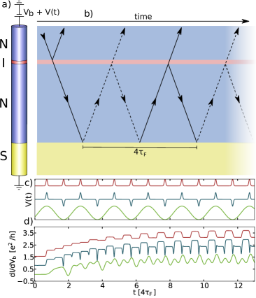
To be specific, we focus on the setup shown in Fig. 1a): a nanowire connected to a superconducting electrode (S, yellow) on one side and to a normal electrode on the other side (N, blue). A short insulating barrier (I, red) (created from either a gate or the Schottky barrier at the semiconductor-electrode interface) serves to confine possible bound states. Without the barrier, these states would hybridize strongly with the continuum. A weak hybridization transforms the bound states into resonances and allows one to probe them by measuring the DC differential conductance through the wire. The superconducting electrode is grounded, while a bias voltage is applied to the normal electrode. is periodic with period .

Scattering theory provides a very intuitive way for understanding Andreev states in terms of an effective Fabry-Perot cavity. Following the approach developed in Ref. Mi et al., 2013, an electron injected from the normal electrode undergoes transmission (reflection) with amplitude () at the barrier and Andreev reflection (an electron is reflected as a hole) at the normal-superconducting interface. The total amplitude for an electron injected from the normal contact being reflected into the contact as a hole (with creation of a Cooper pair inside the superconductor) is given by summing over the different trajectories sketched in Fig. 1b),
| (1) |
The energy is measured from the Fermi energy, . When is smaller than the superconducting gap , is a pure phase given by where for a conventional superconductor and for a topological one Beenakker (2014). The factor accounts for the phase accumulated in the normal region, , where is the time of flight between the superconducting interface and the barrier. The geometric series Eq. (1) can be readily resummed into with,
| (2) |
When the insulating barrier is very high (perfect reflection ) one observes true bound states in the spacer between I and S with energies satisfying with . The zero energy state present for TS is the Majorana bound state Law et al. (2009); Mi et al. (2013). Upon increasing the transparency of the insulating barrier, the Andreev states hybridize with the conducting electrode allowing one to probe them through the differential conductance of the system (note that the TS is spinless, hence the factor 1/2).
The theory for the time-dependent current in the presence of an additional train of pulses follows a very similar line. We first focus on the long junction limit where there are many resonances inside the superconducting gap, . This condition will be relaxed in the numerical computations. Following Refs. Gaury et al., 2014; Gaury and Waintal, 2014 we find the time-dependent electron-hole reflection amplitude to be,
| (3) |
with
| (4) |
where is the additional phase due to the time-dependent potential . This phase is translated by for different trajectories to account for the different times of propagation from the normal contact. It is this phase that will be used to manipulate the resonances. We will consider trains of pulses of different shapes as shown in Fig. 1c). We denote the phase accumulated over one period (upright pulses) or half a period (alternating and sine pulses). In analogy with the DC case, the time-dependent differential conductance is,
| (5) |

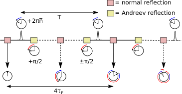
The simplest situation is when one sends a series of upright localized pulses (of widths much shorter than ). Fig. 2 sketches the phase accumulated along the different paths through the junction; it corresponds to a flattened description of the paths shown in Fig. 1b). Whenever one crosses a pulse one picks up a phase , while a phase is picked up upon Andreev reflection at the NS interface (for conventional superconductors; for topological ones, one alternately picks up and , Pikulin et al. (2012)). When the period of the pulse train exactly matches the delay between different trajectories, , the phase is simply given by . As a result, and Eq. (5) takes the form of a geometric series, i.e. the (only) effect of the pulse is to shift the resonance by :
| (6) |
An example of differential conductance for increasing is given in Fig. 3a). In particular, for one transforms the spectrum of a conventional superconductor into the spectrum of a TS and vice versa. Also, for , the train of pulses is equivalent to a train of alternating pulses; Fig. 3b) corresponds to this alternating train. We see that upon increasing (using the amplitude of the pulses), a zero-bias peak develops while the Andreev peaks that were initially present shrink. Fig. 3c) shows the effect of a similar alternating train on a system in the topological phase. We see that the initial zero-bias (Majorana) peak is effectively destroyed when while new Andreev peaks appear; the dual to the previous situation. Anticipating what follows, we find that a simple monochromatic sine pulse (which can be seen as a distortion of the alternating pulse train) will have a similar, although slightly less marked, effect.
To proceed with the generic case where , we expand as a Fourier series, . For a simple monochromatic pulse , the Fourier coefficients are given by where is the Bessel function of the first kind. Keeping only the DC part of the current, we get
| (7) |
The appearance of the resonances in Eq. (7) corresponds to minimizing the denominator, i.e. the phase in the denominator is a multiple of . We thus expect (for ) sharp peaks at positions given by
| (8) |

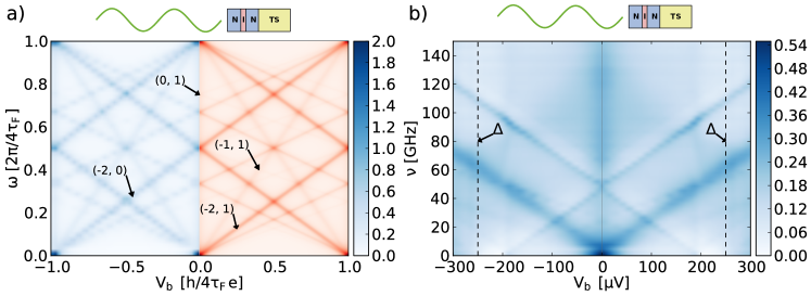
Fig. 4 shows colorplots of the differential conductance for the system in the topological regime in the presence of a sinusoidal time-dependent voltage. The different lines visible on Fig. 4a) correspond to different pairs of the integers and of Eq. (8). It now becomes clear that the presence of the resonant peaks with conductance occur when lines for all values of coincide. Resonant peaks with smaller conductance values occur where subsets of the lines coincide. One can understand each of the terms in Eq. (7) as referring to a -photon absorption process for the resonance. The presence of this characteristic structure in the transport measurements could be used to identify 0-bias peaks as being Andreev/Majorana bound states – as opposed to Kondo resonances or Shiba states, as proposed in Ref. Lee et al., 2012 – as the frequency dependence is closely linked to the time of flight of the resonant cavity, i.e. to the Fabry-Perot nature of the Majorana resonance.
Microscopic (numerical) calculations.
To go beyond the above analytical calculation, we now turn to a microscopic approach following the proposal made in Refs. Chevallier et al. (2013); Oreg et al. (2010). We consider a one dimensional semiconductor wire with (strong) spin-orbit interaction and an external magnetic field. The combination of these two ingredients makes the system effectively spinless close to the Fermi level, so that a nearby (s-wave) superconductor induces p-wave topological superconductivity, and the presence of Majorana fermions in a certain range of parameters (see the supplementary material). The Hamiltonian reads, with where are the electron annihilation (creation) operators with spin up (down) at position . The Effective Bogoliubov-de Gennes Hamiltonian reads,
| (9) | ||||
where is the momentum operator, is the effective mass, is the Zeeman splitting, is the Rashba spin-orbit interaction, is the strength of the tunneling barrier and is the Fermi energy. is the Heaviside step function. The and () are Pauli matrices operating on the spin and particle-hole subspaces respectively. is an on site (Anderson) disorder potential present in the normal part of the wire. The wire is subject to a time-dependent voltage perturbation applied to the normal reservoir (at ) where we assume that the voltage drop is sharp Gaury and Waintal (2014). The superconductor of gap is placed at . The time-dependent perturbation is switched on at . After a transient regime (of approximate duration ) the system relaxes to a periodic regime, see Fig. 1. The DC differential conductance corresponds to the average over one period of the traces shown in Fig. 1d) in the periodic regime. Simulations were carried out using systems discretized on sites and for times up to with the help of the technique described in Ref. Gaury et al. (2014) and of the Kwant package Groth et al. (2014)
We first focus on the simple long junction regime of the analytics. Perfect Andreev reflection, implies (we use in the simulations) while the long junction limit corresponds to (we use ). Fig. 3 [as well as Fig. 4a)] shows a perfect agreement between the simulations (symbols) and the analytical result (lines).
Let us now turn to a regime closer to the experiments performed in the group of KouwenhovenMourik et al. (2012). This implies three important modifications to the above picture. First, the Thouless energy is of the same order as the induced gap in the wire. This is relevant as upon applying the radio-frequency field, many quasi-particles will be excited in the superconductor and one anticipates a corresponding decrease in the amplitude of Andreev reflection. Second, we add disorder to the simulation, corresponding to a mean free path of the same size as the length of the wire (i.e. the system is in the crossover between the ballistic and diffusive regime). Third, the simulations are performed at finite (typical dilution fridge) temperature. These results are shown in Fig. 4b) (see also the supplementary material). We find that the key features of the theory are robust with respect to these perturbations: although the resonances are a bit wider and the thinnest ones have disappeared, the main ones remain perfectly visible. The frequencies required to perform this experiment are within reach of current commercially available apparatus.
Conclusion.
We have shown that the interplay between a train of pulses and Andreev/Majorana states can provide a differential conductance identical to the DC case except for a tunable dynamical phase (upright pulses) as well as a spectroscopy of the states (sine pulses). Beyond the present study, we anticipate that the same line of thought could be used for more elaborate manipulations such as those needed for quantum computation.
Acknowledgements
This work was supported by the ERC grant MESOQMC from the European Union. We thank M. Houzet and J. Meyer for interesting discussions.
References
- Nayak et al. (2008) C. Nayak, S. H. Simon, A. Stern, M. Freedman, and S. Das Sarma, Rev. Mod. Phys. 80, 1083 (2008).
- Kitaev (2001) A. Y. Kitaev, Phys.-Usp. 44, 131 (2001), .
- Ivanov (2001) D. A. Ivanov, Phys. Rev. Lett. 86, 268 (2001).
- Fu and Kane (2008) L. Fu and C. L. Kane, Phys. Rev. Lett. 100, 096407 (2008).
- Mi et al. (2013) S. Mi, D. I. Pikulin, M. Wimmer, and C. W. J. Beenakker, Phys. Rev. B 87, 241405 (2013).
- Lutchyn et al. (2010) R. M. Lutchyn, J. D. Sau, and S. Das Sarma, Phys. Rev. Lett. 105, 077001 (2010).
- Oreg et al. (2010) Y. Oreg, G. Refael, and F. von Oppen, Phys. Rev. Lett. 105, 177002 (2010).
- Das et al. (2012) A. Das, Y. Ronen, Y. Most, Y. Oreg, M. Heiblum, and H. Shtrikman, Nat Phys 8, 887 (2012), .
- Mourik et al. (2012) V. Mourik, K. Zuo, S. M. Frolov, S. R. Plissard, E. P. a. M. Bakkers, and L. P. Kouwenhoven, Science 336, 1003 (2012), .
- Deng et al. (2012) M. T. Deng, C. L. Yu, G. Y. Huang, M. Larsson, P. Caroff, and H. Q. Xu, Nano Lett. 12, 6414 (2012), .
- Churchill et al. (2013) H. O. H. Churchill, V. Fatemi, K. Grove-Rasmussen, M. T. Deng, P. Caroff, H. Q. Xu, and C. M. Marcus, Phys. Rev. B 87, 241401 (2013).
- Jiang et al. (2011) L. Jiang, T. Kitagawa, J. Alicea, A. R. Akhmerov, D. Pekker, G. Refael, J. I. Cirac, E. Demler, M. D. Lukin, and P. Zoller, Phys. Rev. Lett. 106, 220402 (2011).
- Liu et al. (2012a) G. Liu, N. Hao, S.-L. Zhu, and W. M. Liu, Phys. Rev. A 86, 013639 (2012a).
- Liu et al. (2013) D. E. Liu, A. Levchenko, and H. U. Baranger, Phys. Rev. Lett. 111, 047002 (2013).
- Kundu and Seradjeh (2013) A. Kundu and B. Seradjeh, Phys. Rev. Lett. 111, 136402 (2013).
- Pikulin et al. (2012) D. I. Pikulin, J. P. Dahlhaus, M. Wimmer, H. Schomerus, and C. W. J. Beenakker, New J. Phys. 14, 125011 (2012), .
- Lee et al. (2012) E. J. H. Lee, X. Jiang, R. Aguado, G. Katsaros, C. M. Lieber, and S. De Franceschi, Phys. Rev. Lett. 109, 186802 (2012).
- Chang et al. (2013) W. Chang, V. E. Manucharyan, T. S. Jespersen, J. Nygård, and C. M. Marcus, Phys. Rev. Lett. 110, 217005 (2013).
- Cheng et al. (2014) M. Cheng, M. Becker, B. Bauer, and R. M. Lutchyn, Phys. Rev. X 4, 031051 (2014).
- Žitko et al. (2015) R. Žitko, J. S. Lim, R. López, and R. Aguado, Phys. Rev. B 91, 045441 (2015).
- Liu et al. (2012b) J. Liu, A. C. Potter, K. T. Law, and P. A. Lee, Phys. Rev. Lett. 109, 267002 (2012b).
- Lutchyn et al. (2011) R. M. Lutchyn, T. D. Stanescu, and S. Das Sarma, Phys. Rev. Lett. 106, 127001 (2011).
- Kells et al. (2012a) G. Kells, D. Meidan, and P. W. Brouwer, Phys. Rev. B 85, 060507 (2012a).
- Lee et al. (2014) E. J. H. Lee, X. Jiang, M. Houzet, R. Aguado, C. M. Lieber, and S. De Franceschi, Nat Nano 9, 79 (2014), .
- Rieder et al. (2012) M.-T. Rieder, G. Kells, M. Duckheim, D. Meidan, and P. W. Brouwer, Phys. Rev. B 86, 125423 (2012).
- Stanescu and Tewari (2014) T. D. Stanescu and S. Tewari, Phys. Rev. B 89, 220507 (2014).
- Kells et al. (2012b) G. Kells, D. Meidan, and P. W. Brouwer, Phys. Rev. B 86, 100503 (2012b).
- Roy et al. (2013) D. Roy, N. Bondyopadhaya, and S. Tewari, Phys. Rev. B 88, 020502 (2013).
- Beenakker (2014) C. W. J. Beenakker, arXiv:1407.2131 [cond-mat] (2014), arXiv: 1407.2131.
- Law et al. (2009) K. T. Law, P. A. Lee, and T. K. Ng, Phys. Rev. Lett. 103, 237001 (2009).
- Gaury et al. (2014) B. Gaury, J. Weston, M. Santin, M. Houzet, C. Groth, and X. Waintal, Physics Reports 534, 1 (2014), .
- Gaury and Waintal (2014) B. Gaury and X. Waintal, Nat Commun 5 (2014).
- Chevallier et al. (2013) D. Chevallier, P. Simon, and C. Bena, Phys. Rev. B 88, 165401 (2013).
- Groth et al. (2014) C. W. Groth, M. Wimmer, A. R. Akhmerov, and X. Waintal, New J. Phys. 16, 063065 (2014), .