Longitudinal spin Seebeck effect contribution in transverse spin Seebeck effect experiments in Pt/YIG and Pt/NFO
Abstract
We investigate the inverse spin Hall voltage of a thin Pt strip deposited on the magnetic insulators \ceY3Fe5O12 (YIG) and \ceNiFe2O4 (NFO) with a temperature gradient in the film plane. We observe characteristics typical of the spin Seebeck effect, although we do not observe a change of sign of the voltage at the Pt strip when it is moved from hot to cold side, which is believed to be the most striking feature of the transverse spin Seebeck effect. Therefore, we relate the observed voltages to the longitudinal spin Seebeck effect generated by a parasitic out-of-plane temperature gradient, which can be simulated by contact tips of different material and heat conductivities and by tip heating. This work gives new insights into the interpretation of transverse spin Seebeck effect experiments, which are still under discussion.
Spin caloritronics is an active branch in spintronics Bauer et al. (2012); Wolf et al. (2001). The interplay between heat, charge and spin transport opens a new area of fascinating issues involving the use of waste heat in electronic devices. One potentially useful effect for heat harvesting Kirihara et al. (2012) is the spin Seebeck effect (SSE) Uchida et al. (2008) which was observed in 2008.
It was reported that a spin current perpendicular to an applied temperature gradient can be generated in a ferromagnetic metal (FMM) by the transverse spin Seebeck effect (TSSE) Uchida et al. (2008). An adjacent normal metal (NM) converts the spin current via the inverse spin Hall effect (ISHE) Saitoh et al. (2006) into a transverse voltage, which is antisymmetric with respect to the external magnetic field (, cf. Fig. 1 (a)). In this geometry, the temperature gradient is typically aligned in-plane () and can also induce a planar Nernst effect (PNE) in FMM with magnetic anisotropy Avery et al. (2012) which is due to the anisotropic magnetic thermopower and symmetric with respect to (). For pure in a ferro(i)magnetic insulator (FMI) there is no PNE, since there are no free charge carriers available. However, if the NM material is close to the Stoner criterion, a static magnetic proximity effect could induce a so called proximity PNE, which in general is present in spin polarized NM adjacent to a FMM and could also occur in a NM-FMI contact (cf. Fig. 1 (a)).
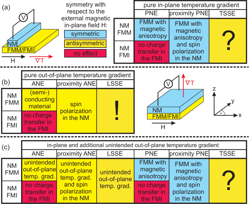
For the longitudinal SSE (LSSE) Uchida et al. (2010a) the spin current flows directly from the FM into an adjacent NM parallel to the temperature gradient (cf. Fig. 1 (b)), which is typically aligned out-of-plane (). In NM/FMM bilayers the anomalous Nernst effect (ANE) can occur, but is absent in the FMI. In semiconducting materials the ANE contributes to the LSSE as already shown for Pt/NFO at room temperature Meier et al. (2013a). Additionally, if the NM would be spin polarized by the proximity to the FM, an additional proximity ANE could occur Guo et al. (2014) (cf. Fig. 1 (b)).
We would like to point out that Figs. 1 (a) and 1 (b) include results of previous experiments with pure on NM/FMM Uchida et al. (2008); Jaworski et al. (2010); Avery et al. (2012); Meier et al. (2013b) and on NM/FMI Uchida et al. (2010a) as well as pure on NM/FMM Meier et al. (2013a) and on NM/FMI Uchida et al. (2010b, c); Huang et al. (2012); Weiler et al. (2012); Qu et al. (2013); Kehlberger et al. (2014); Siegel et al. (2014); Agrawal et al. (2014). As summarized in Fig. 1 (c) an unintended can hamper the evaluation of TSSE experiments with applied . Heat flow into the surrounding area or through the electrical contacts can induce an additional ANE in NM/FMM bilayers and NM/magnetic semiconductors as discussed in literature Bosu et al. (2011); Huang et al. (2011); Schmid et al. (2013); Meier et al. (2013b); Bui and Rivadulla (2014); Soldatov et al. (2014). But since, in principle, all the effects of an LSSE experiment can be present in the TSSE experiment with unintended , proximity Nernst effects and especially parasitic LSSE can also be present in NM/FMI bilayers as already mentioned recently Schreier et al. (2013). This leads to four possible effects which are antisymmetric with respect to the external magnetic field, when the temperature gradient is not controlled very carefully (cf. Fig. 1 (c)). These phenomena and discussions of side-effects in TSSE experiments have not been treated systematically in the literature up to now for NM/FMI bilayers and will be investigated in this study.
The YIG films in our experiments had a thickness of and were deposited on gadolinium gallium garnet (\ceGd3Ga5O12, GGG) (111)-oriented single crystal substrates with width and length by pulsed laser deposition (PLD) from a stoichiometric polycrystalline target. The films show a coercive field of about and a saturation magnetization of . The \ceNFO films with a thickness of about were deposited on \ceMgAl2O4 (\ceMAO) (100)-oriented substrates by direct liquid injection chemical vapor deposition (DLI-CVD)Li et al. (2011); Meier et al. (2013a). After a vacuum break and cleaning with ethanol in an ultrasonic bath a thin Pt strip was deposited by dc magnetron sputtering in an Ar atmosphere of through a wide split-mask on one sample side of the \ceYIG and \ceNFO films with a length of .
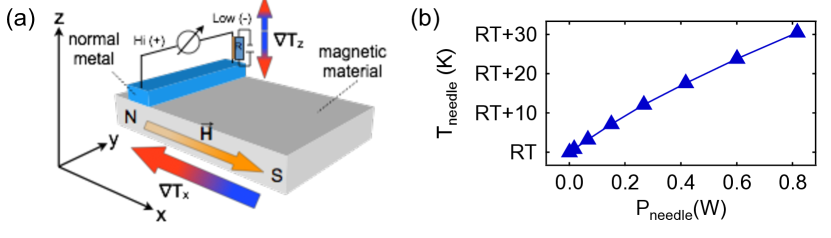
For the experiments we used the same setup and technique described in Ref. Meier et al. (2013b). The experiments are conducted under ambient conditions and the ends of the Pt strip were contacted with a microprobe system with Au and W tips of different diameters. Furthermore, one set of Au tips was equipped with a resistor for heating the tip to intentionally induce a (cf. Fig. 2 (a)) Meier et al. (2013b). Fig. 2 (b) shows the nearly linear relation between the power dissipated in the resistor and the tip temperature as determined with a type-K thermocouple glued to the tip in a calibration measurement. The voltage at the Pt strip was measured with a Keithley 2182A nanovoltmeter. An external magnetic field was applied along x in a range of for \ceYIG and of for \ceNFO films.
First, the ISHE voltage from the Pt/YIG sample was measured for various . The Pt strip was on the hot side and contacted with W tips. The voltage shows no significant variation within the sensitivity limit when is varied (Fig. 3 (a)). No Nernst effects are observed due to the insulating magnetic layer and no evidence for an additional can be detected. Therefore, the clamping and heating of the sample in our setup and the contacting with thin W tips results in a pure as already shown in Ref. Meier et al. (2013b). TSSE is not observable although the Pt strip is located near the hot side of the YIG film and far away from the center where the TSSE should vanish.
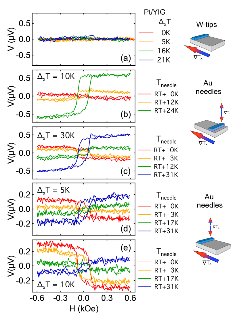
In the next step we created a second heat sink by using thicker Au tips (Fig. 3 (b)). The diameter of the contact area is of about in contrast to the contact area with W tips of about . It can be seen that the measured voltage now shows an antisymmetric behavior with respect to magnetic field inversion (Fig. 3 (b)-(e)). Next, we applied a voltage to the Au tip resistor to heat the needle and change the out-of-plane heat flow. The heated Au needle is labeled = RT + x with room temperature RT = . The magnitude (the voltage in saturation) is calculated with for the average voltage in the region of and for Pt/YIG as well as and for Pt/NFO, respectively.
In Fig. 3 (b) for a small antisymmetric effect of about is obtained when the Pt strip is at the cold side of the YIG film. When the needle is heated to the ISHE voltage changes its sign to a value of and changes further to for . By using these Au needles with large contact areas an additional small out-of-plane heat flow is generated even at the cold side of the sample. This heat flow changes its sign with increasing which can be detected by the sign reversal of the measured voltage. When is increased ( in Fig. 3 (c)) the ISHE voltage at the Pt is for and therefore three times larger than for . The ISHE voltage again increases with increasing and changes sign.
For a Pt strip at the hot side without tip heating is larger than at the cold side. For the magnitude is about (Fig. 3 (d)) which can be decreased to for (Fig. 3 (e)). The sign and the magnitude of can also be controlled by and, therefore, by . When is fixed at , is about for and for .
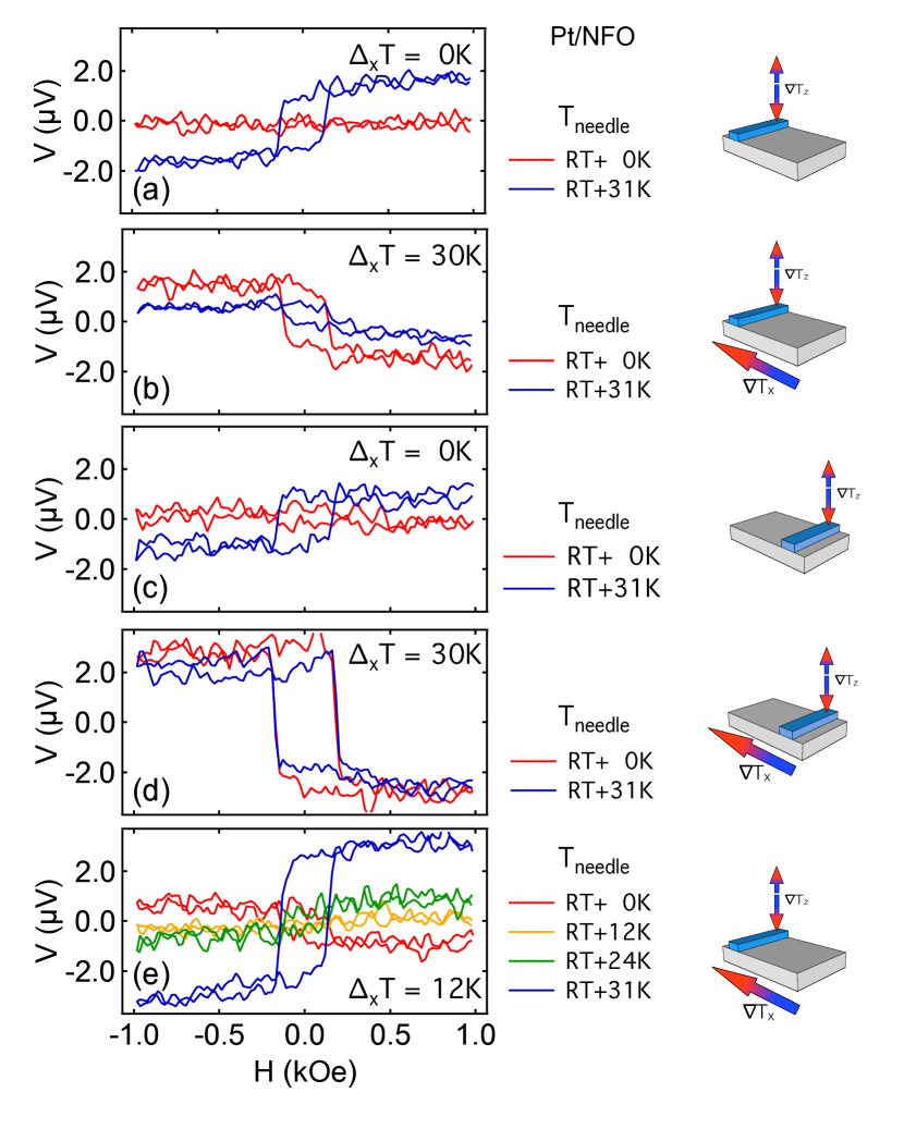
For a verification of this behavior in another material system, \ceNFO films with a Pt strip were used and contacted with Au needles. When and no tip heating is applied no significant change in as a function of is observed (Fig. 4 (a)). This behavior is the same for Pt strips on both sides of the \ceNFO film (Fig. 4 (c)).
When a is applied, the same sign of on both sides is achieved (Fig. 4 (b),(d)). The effect can again be manipulated by applying a needle temperature of . The discrepancy for Pt/NFO measurements on hot side (smaller , Fig. 4 (b)) and cold side (larger , Fig. 4 (d)) compared to Pt/YIG on hot side (larger , Fig. 3 (e)) and cold side (smaller , Fig. 3 (b)) can be explained by contacting the needles again after reversing the sample to ”move” the Pt strip from the hot to the cold side. The real contact area between the tips and the Pt can be different when the sample is remounted. Furthermore, was varied for (Fig. 4 (e)). at is about . The absolute value is more than two times smaller than for () with the change of . also vanishes for and changes sign for increasing .
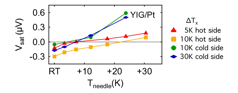
measured for Pt/YIG at the hot and cold side is plotted as a function of for different in Fig. 5. A non-heated Au needle results in the same sign of for all , while is smaller on the cold side compared to the hot side. We explain this behaviour of by an unintended heat flux through the Au needles leading to a vertical temperature gradient and, therefore, to a LSSE induced spin current into the Pt. We point out, that the sign of the resulting voltage at the Pt strip is quantitatively consistent with the magnitude of the recent LSSE reported by Schreier et al. Schreier et al. (2014) from comparative experiments performed in different groups if we consider an unintended out-of-plane pointing into -z direction. For a heated Au needle increases and crosses zero (cf. Fig. 5). Here, the tip heating compensates the out-of-plane heat flux induced by (). After the sign change of (and therefore, ), the values increases with a larger (smaller) slope for the cold (hot) side.
Xiao et al. Xiao et al. (2010) discussed the temperature difference between the magnon temperature in the FM and the electron temperature in the NM as the origin of the thermally induced spin current. can be inferred from the recorded voltage as Xiao et al. (2010); Schreier et al. (2013)
| (1) |
Here, is the magnetic coherence volume, is the real part of the spin mixing conductance, is the gyromagnetic ratio, is the Boltzmann constant, is the elementary charge, is the spin Hall angle, and is the spin diffusion length of the NM material. The two temperature model has proven successful in relating to the phonon temperature, accessible in experiments Schreier et al. (2013); Flipse et al. (2012). We simulate the phonon and magnon temperatures assuming 1D transport in our films and disregard the influence of thermal contact resistance other than the coupling between magnons and electrons. This yields a value , the (phonon) temperature drop across the YIG film, for which the experimentally measured is obtained. We assume . All material dependent YIG parameters were taken from Ref. Schreier et al. (2013).
We calculated for the largest and smallest taken from Fig. 5 at RT (red curves in Fig. 3 (b) and (e)) and the corresponding . For (cf. Fig. 3 (b)) we obtain and a corresponding . For (cf. Fig. 3 (e)) the corresponding values are and . The obtained are in the order of a few millikelvins. It is reasonable to assume that such values can be induced by e.g. thick contact tips, especially considering that our initial simplifications should lead to an overestimation of Schreier et al. (2013). The transverse spin Seebeck configuration was investigated in detail in Ref. Schreier et al. (2013). It was found that for the obtained is well below , even at the very edge of the sample where is maximized. This further supports the notion that spurious out-of-plane gradients are responsible for the voltages observed in our samples.
The different magnitudes in voltage for Pt/NFO compared to Pt/YIG can be explained by different contact areas of the tips, different thicknesses and thermal conductivities between NFO and YIG as well as different spin mixing conductances Weiler et al. (2013); Qiu et al. (2013). However, for both sample systems the spin mixing conductance should be large enough to observe a thermally driven spin current across the NM/FMI interface, since we clearly observe an LSSE due to the Au tip heating induced .
In addition to the LSSE, we now discuss other parasitic effects like the ANE and proximity ANE, which can be produced by an unintended (see Fig. 1). We can exclude an ANE for YIG due to the lack of charge carriers. For NFO we observed an ANE which is one order of magnitude smaller at RT than the LSSE Meier et al. (2013a). This ANE can be explained by the weak conductance of NFO at RT due to thermal activation energies of a few hundred meV depending on the preparation technique Meier et al. (2013a); Klewe et al. (2014). The proximity ANE in Pt/NFO can also be excluded, since no spin polarization was found using x-ray resonant magnetic reflectivity (XRMR) measurements, which are very sensitive to the interface spin polarization Kuschel et al. (2014). In case of Pt/YIG Geprägs et al. presented x-ray magnetic circular dichroism measurements (XMCD) with no evidence for any spin polarization in Pt Geprägs et al. (2012), while Lu et al. could show XMCD measurements indicating magnetic moments in Pt on their YIG samples Lu et al. (2013). Future investigations with XRMR can give more insight to this discrepancy. However, Kikkawa et al. could show that a potential contribution of a proximity ANE additional to the LSSE is negligibly small Kikkawa et al. (2013). This supports our conclusion, that the main antisymmetric contribution in our measurements on both Pt/YIG and Pt/NFO is the LSSE, which is driven by an out-of-plane temperature gradient.
We do not observe any symmetric contribution for without tip heating. Therefore, PNE and proximity PNE contributions can also be excluded. Nevertheless, we find a small symmetric contribution for strong tip heating as demonstrated in Fig. 3 (c) for . In the region of small peaks are visible under symmetrization of the voltage. This hints at the existence of an additional magnetothermopower effect potentially induced by a temperature gradient and will be part of future investigations.
Recently, Wegrowe et al. Wegrowe et al. (2014) used anisotropic heat-transport as an interpretation for the measured voltages using in-plane temperature gradients. In their work, they derived the anisotropic field-dependent temperature gradient in FMM and FMI from the Onsager reciprocity relations. Therefore, the thermocouple effect between the FM, the NM and the contacting tips can generate field-dependent voltages if there is a difference in the Seebeck coefficients. In our investigated systems, the Seebeck coefficients are indeed different for FM, Pt and the contact tips. However, since we do not observe a field-dependent variation of the ISHE voltage by using W tips, any anisotropic field-dependent heat-transport can be excluded as the reason for the observed voltages.
In summary, we investigated the relevance of TSSE in Pt/YIG and Pt/NFO systems. We found no significant ISHE voltages upon applying an in-plane temperature gradient and using sharp W tips ( contact diameter) for the electrical contacting. However, upon using tips with more than diameter contact area, which induce an additional out-of-plane temperature gradient, an antisymmetric contribution to the ISHE voltage of the Pt strip could be introduced at will. This antisymmetric effect can be identified as LSSE which was verified by controlling the needle temperature and varying the out-of-plane temperature gradient. Taken together, in all our experiments, we thus only observe LSSE-type signatures. These LSSE voltages can be reminiscent of a TSSE-type response if an unintentional (or intentional) is present. This shows that utmost care is required if one is to interpret magnetothermopower effects in terms of the TSSE.
We thank the DFG (SPP 1538) and the EMRP JRP EXL04 SpinCal for financial support. The EMRP is jointly funded by the EMRP participating countries within EURAMET and the EU.
References
- Bauer et al. (2012) G. E. W. Bauer, E. Saitoh, and B. J. van Wees, Nature Materials 11, 391 (2012).
- Wolf et al. (2001) S. A. Wolf, D. D. Awschalom, R. A. Buhrman, J. M. Daughton, S. von Molnár, M. L. Roukes, A. Y. Chtchelkanova, and D. M. Treger, Science 294, 1488 (2001).
- Kirihara et al. (2012) A. Kirihara, K. Uchida, Y. Kajiwara, M. Ishida, Y. Nakamura, T. Manako, E. Saitoh, and S. Yorozu, Nature Materials 11, 686 (2012).
- Uchida et al. (2008) K. Uchida, S. Takahashi, K. Harii, J. Ieda, W. Koshibae, K. Ando, S. Maekawa, and E. Saitoh, Nature 455, 778 (2008).
- Saitoh et al. (2006) E. Saitoh, M. Ueda, H. Miyajima, and G. Tatara, Applied Physics Letters 88, 182509 (2006).
- Avery et al. (2012) A. Avery, M. Pufall, and B. Zink, Physical Review Letters 109, 196602 (2012).
- Uchida et al. (2010a) K. Uchida, H. Adachi, T. Ota, H. Nakayama, S. Maekawa, and E. Saitoh, Applied Physics Letters 97, 172505 (2010a).
- Meier et al. (2013a) D. Meier, T. Kuschel, L. Shen, A. Gupta, T. Kikkawa, K. Uchida, E. Saitoh, J. M. Schmalhorst, and G. Reiss, Physical Review B 87, 054421 (2013a).
- Guo et al. (2014) G. Y. Guo, Q. Niu, and N. Nagaosa, Physical Review B 89, 214406 (2014).
- Jaworski et al. (2010) C. M. Jaworski, J. Yang, S. Mack, D. D. Awschalom, J. P. Heremans, and R. C. Myers, Nature Materials 9, 898 (2010).
- Meier et al. (2013b) D. Meier, D. Reinhardt, M. Schmid, C. H. Back, J. M. Schmalhorst, T. Kuschel, and G. Reiss, Physical Review B 88, 184425 (2013b).
- Uchida et al. (2010b) K. Uchida, H. Adachi, T. Ota, H. Nakayama, S. Maekawa, and E. Saitoh, Applied Physics Letters 97, 172505 (2010b).
- Uchida et al. (2010c) K. Uchida, T. Nonaka, T. Ota, and E. Saitoh, Applied Physics Letters 97, 262504 (2010c).
- Huang et al. (2012) S. Y. Huang, X. Fan, D. Qu, Y. P. Chen, W. G. Wang, J. Wu, T. Y. Chen, J. Q. Xiao, and C. L. Chien, Physical Review Letters 109, 107204 (2012).
- Weiler et al. (2012) M. Weiler, M. Althammer, F. Czeschka, H. Huebl, M. Wagner, M. Opel, I.-M. Imort, G. Reiss, A. Thomas, R. Gross, and S. Goennenwein, Physical Review Letters 108, 106602 (2012).
- Qu et al. (2013) D. Qu, S. Y. Huang, J. Hu, R. Wu, and C. L. Chien, Physical Review Letters 110, 067206 (2013).
- Kehlberger et al. (2014) A. Kehlberger, G. Jakob, M. C. Onbasli, D. H Kim, C. A. Ross, and M. Kläui, Journal of Applied Physics 115, 17C731 (2014).
- Siegel et al. (2014) G. Siegel, M. C. Prestgard, S. Teng, and A. Tiwari, Scientific Reports 4 (2014).
- Agrawal et al. (2014) M. Agrawal, V. I. Vasyuchka, A. A. Serga, A. Kirihara, P. Pirro, T. Langner, M. B. Jungfleisch, A. V. Chumak, E. T. Papaioannou, and B. Hillebrands, Physical Review B 89, 224414 (2014).
- Bosu et al. (2011) S. Bosu, Y. Sakuraba, K. Uchida, K. Saito, T. Ota, E. Saitoh, and K. Takanashi, Physical Review B 83 (2011).
- Huang et al. (2011) S. Huang, W. Wang, S. Lee, J. Kwo, and C. Chien, Physical Review Letters 107, 196602 (2011).
- Schmid et al. (2013) M. Schmid, S. Srichandan, D. Meier, T. Kuschel, J. M. Schmalhorst, M. Vogel, G. Reiss, C. Strunk, and C. H. Back, Physical Review Letters 111, 187201 (2013).
- Bui and Rivadulla (2014) C. T. Bui and F. Rivadulla, Phys. Rev. B 90, 100403 (2014).
- Soldatov et al. (2014) I. V. Soldatov, N. Panarina, C. Hess, L. Schultz, and R. Schäfer, Phys. Rev. B 90, 104423 (2014).
- Schreier et al. (2013) M. Schreier, A. Kamra, M. Weiler, J. Xiao, G. E. W. Bauer, R. Gross, and S. T. B. Goennenwein, Phys. Rev. B 88, 094410 (2013).
- Li et al. (2011) N. Li, Y.-H. A. Wang, M. N. Iliev, T. M. Klein, and A. Gupta, Chemical Vapor Deposition 17, 261 (2011).
- Schreier et al. (2014) M. Schreier, G. E. W. Bauer, V. Vasyuchka, J. Flipse, K. Uchida, J. Lotze, V. Lauer, A. Chumak, A. Serga, S. Daimon, T. Kikkawa, E. Saitoh, B. J. van Wees, B. Hillebrands, R. Gross, and S. T. B. Goennenwein, arXiv:1404.3490 (2014).
- Xiao et al. (2010) J. Xiao, G. Bauer, K. Uchida, E. Saitoh, and S. Maekawa, Physical Review B 81 (2010).
- Flipse et al. (2012) J. Flipse, F. L. Bakker, A. Slachter, F. K. Dejene, and B. J. van Wees, Nature Nanotechnology 7, 166 (2012).
- Weiler et al. (2013) M. Weiler, M. Althammer, M. Schreier, J. Lotze, M. Pernpeintner, S. Meyer, H. Huebl, R. Gross, A. Kamra, J. Xiao, Y.-T. Chen, H. Jiao, G. E. W. Bauer, and S. T. B. Goennenwein, Physical Review Letters 111, 176601 (2013).
- Qiu et al. (2013) Z. Qiu, K. Ando, K. Uchida, Y. Kajiwara, R. Takahashi, H. Nakayama, T. An, Y. Fujikawa, and E. Saitoh, Applied Physics Letters 103, 092404 (2013).
- Klewe et al. (2014) C. Klewe, M. Meinert, A. Boehnke, K. Kuepper, E. Arenholz, A. Gupta, J. M. Schmalhorst, T. Kuschel, and G. Reiss, Journal of Applied Physics 115, 123903 (2014).
- Kuschel et al. (2014) T. Kuschel, C. Klewe, J. M. Schmalhorst, F. Bertram, O. Schuckmann, T. Schemme, J. Wollschläger, S. Francoual, J. Strempfer, A. Gupta, M. Meinert, G. Götz, D. Meier, and G. Reiss, arXiv:1411.0113 (2014).
- Geprägs et al. (2012) S. Geprägs, S. Meyer, S. Altmannshofer, M. Opel, F. Wilhelm, A. Rogalev, R. Gross, and S. T. B. Goennenwein, Applied Physics Letters 101, 262407 (2012).
- Lu et al. (2013) Y. Lu, Y. Choi, C. Ortega, X. Cheng, J. Cai, S. Huang, L. Sun, and C. Chien, Physical Review Letters 110, 147207 (2013).
- Kikkawa et al. (2013) T. Kikkawa, K. Uchida, Y. Shiomi, Z. Qiu, D. Hou, D. Tian, H. Nakayama, X. F. Jin, and E. Saitoh, Physical Review Letters 110, 067207 (2013).
- Wegrowe et al. (2014) J. E. Wegrowe, H. J. Drouhin, and D. Lacour, Physical Review B 89, 094409 (2014).