Topological p-n junctions in helical edge states
Abstract
Quantum spin Hall effect is endowed with topologically protected edge modes with gapless Dirac spectrum. Applying a magnetic field locally along the edge leads to a gapped edge spectrum with opposite parity for winding of spin texture for conduction and valence band. Using Pancharatnam’s prescription for geometric phase it is shown that mismatch of this parity across a - junction, which could be engineered into the edge by electrical gate induced doping, leads to a phase dependence in the two-terminal conductance which is purely topological (0 or ). This fact results in a classification of such junctions with an associated duality. Current asymmetry measurements which are shown to be robust against electron-electron interactions are proposed to infer this topology.
pacs:
03.65.Vf, 73.20.-r, 73.43.-f, 85.75.-dIntroduction : In a seminal paperBerry (1984), Berry introduced the cyclic and adiabatic geometric phase that had implications across disciplinesShapere and Wilczek (1989) ranging from high energy physics to condensed matter physics. It was soon realized that both the conditions of adiabaticityNakagawa (1987); Aharonov and Anandan (1987) as well as cyclicity of evolutionSamuel and Bhandari (1988) were not at all necessary and the geometric phase was a property of the Hilbert space itself. It turned out that a generalized version of this idea was anticipatedRamaseshan and Nityananda (1986); Berry (1987) by Pancharatnam in his pioneering work on interference of classical light in distinct states of polarizationPancharatnam (1956). Pancharatnam’s connection (or rule) gives a natural way to compare the relative phases between any two non-orthogonal states, and . If is real and positive, they are said to be “in phase” or “parallel”. For a two-state quantum system, if we consider three arbitrary non-orthogonal states such that pair-wise and are in phase, it turns out is not necessarily in phase with . Deviation of being in phase with is quantified in terms of phase of the complex number . This phase is given by half the solid angle of the geodesic triangle subtended at the centre of the Bloch sphere.
We show that transport in helical 1D electron gas (1DEG)Wu et al. (2006) with Dirac-like spectrum is dominated by geometric phase of the type described above when a gap is opened up in the spectrum due to application of magnetic field while transport is induced in the gapped spectrum by pure electrical doping. The spin-momentum locked helical states are believed to be of potential importance for future spintronics device applicationsYokoyama and Murakami (2014), hence an understanding of transport from a geometric phase point of view in presence of standard probes such as magnetic field or electric field could provide useful guidelines for efficient manipulation of these states for such applications. In this article we show that electrical transport across -, -, -, - junctions designed into the helical edge have a topological classification which essentially stems from Pancharatnam’s prescription of geometric phase and has its origin in spin-momentum locked nature of the gapless spectrum. Here p and n corresponds to hole and electron type doping. We also show that this topological description of the junction facilitates an effective conversion of - - (as far as the electrical transport properties of these junctions are concerned) not by changing the doping but by suitably manipulating the magnetic field acting on them, hence opening up new possibilities for manipulation of these junctions. Finally we discuss the experimental feasibility of our proposal when the 1D helical state is hosted on the edge of a quantum spin Hall state that was experimentally observed in HgTe/CdTe quantum wellsKönig et al. (2007).
Model :
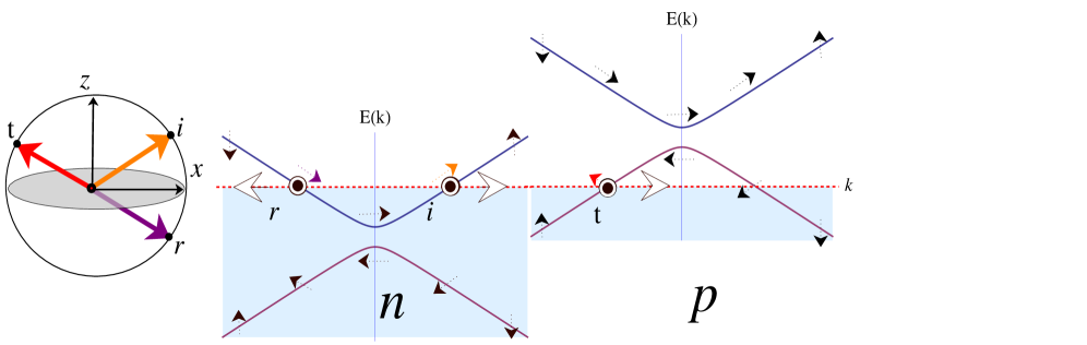
We consider a 1-D helical state physically lying along the -axis with its spin-orbit (SO) field pointing along -axis which is exposed to external applied magnetic field and gate electrodes imposed electric field. The Hamiltonian is given by
| (1) |
where is the reduced Planck constant, is the Fermi velocity, are the Pauli matrices, is the spin operator, is the Landé-g factor for the electron, is the Bohr magneton, is the electronic charge and is the applied gate voltage. Gating induced electrostatic potentials are assumed to be acting independently on the two halves ( and ) respectively. These electrostatic potentials allow for independent tuning of each patch either to electron-type or to hole-type doping. The external applied magnetic field profile acting on the 1-D helical state is taken to be
| (2) |
Application of magnetic field along any direction in - plane opens up a gap in the dispersionSoori et al. (2012) while selecting different in-plane directions for the -field in the two patches allows for manipulation of the Pancharatnam geometric phase in a desired way as we will see later.
Landauer conductance : The energy spectrum for the problem in each semi-infinite patch is given by where and is the momentum of the electron. The corresponding momentum dependent eigen-spinor is given by
| (3) |
where is the normalization constant, stands for conduction and valence band respectively. Now by demanding continuity of the plane-wave solution of the Schrdinger equation at the junction we obtain the Landauer conductance in the linear response limit which is expressed in terms of transmission probability as
| (4) |
where, , the parameters , and are the spinor overlaps given by , , where the indices stand for the incident, reflected and transmitted spinors respectively evaluated at the average Fermi energy across the junction. The exact expressions for and would depend upon which decides the doping on the two sides of the junction and the relative angle between the applied magnetic fields, via Eq.3. and are the density of states of the incident(reflected) branch and the transmitted branch given by , . And is the Pancharatnam geometric phase as defined in the introduction which is the phase of the complex number Berry (1987).
Note that the two-terminal linear conductance across the junction (Eq.4) depends upon two quantities : (a) the mismatch of density of states across the junction at the Fermi level, and (b) which only depends on the spin texture mismatch of the dispersion across the junction at the Fermi level. The non-trivial aspect of the spin-texture mismatch lies in its dependence on which is actually the only phase which influences the two terminal conductance. Next, we analyze the influence of on the electrical transport.
Topological phase in case and the index : For , the magnetic field points only along the -direction while the SO field points along -axis, hence the points representing incident, reflected and the transmitted spinors on the Bloch sphere are restricted to lie on a great circle contained in - plane irrespective of the details of doping. As a consequence, the spherical triangle formed by connecting these three points (on the Bloch sphere) along the geodesic pathSamuel and Bhandari (1988) governed by details of has two distinct possibilities : either they encircle the centre of Bloch sphere once (call it ) or it goes back and forth on a finite patch of the great circle (call it ) (see also Mehta (2009a); Longuet-Higgins
et al. (1958)) without encircling the centre. The solid angle subtended by the closed curve at the centre is and that enclosed by is zero respectively. Using Pancharatnam’s idea, we can immediately predict that , which is the phase of , should be equal to half the solid angleBerry (1987) subtended by the geodesic triangles at the centre of Bloch sphere. This implies that should correspond to and should correspond to respectively, i. e. is real and negative and is real and positive. Now, type of closed path which encircles the centre of Bloch sphere once are topologically distinct from that of type of path which do not encircle it at all and this fact manifests itself as sign of in the transmission amplitude. It is worth noting that all closed paths restricted to the - plane that are winding the origin of Bloch sphere even number of times are equivalent as the geometric phase associated with these paths are zero modulo . Hence they are all equivalent to . While all closed paths that are winding the origin of Bloch sphere odd number of times are equivalent as the geometric phase associated with these paths are modulo and hence they are equivalent to . This facts imply that the conductance corresponding to the case of and can be distinguished in terms of a index given by
| (5) |
where takes two distinct inequivalent values given by ( for ) and ( for ). To develop an understanding of the physical situations that should correspond to and , we define a parity of winding of the spin-texture for left and right moving electrons in the conduction and the valence band given by
| (6) |
where is defined in Eq.3 and for right and left movers respectively. where is the expectation value of the components of the spin operator. This is an interesting quantity as it tells us which way is the spin twisting as we move from to in the conduction and the valence band. Note that as , the SO field dominates over external B-field and dictates the orientation of spin associated with the momentum mode while at the SO field vanishes and spin direction is dictated by the externally applied magnetic field. Essentially these two facts decide the parity, . It is straight-forward to check that all junctions which have an opposite sign of for electrons of a given chirality (right or left movers) at the Fermi level on two sides of the junction always correspond to the (see Fig.2 in supplementary material) case. Hence this situation corresponds to the case. This is the case for - and - junctions. On the other hand, if parity () is same on two sides of the junction (i. e. - and - junctions) then it always correspond to and hence corresponds to case. This observation completes the topological classification of such junctions with negative value for the index for -, - junctions and positive value for the index for -, - junctions. This is one of the central results of this article. Next we show that this topological phase () becomes geometric as we turn on a finite .
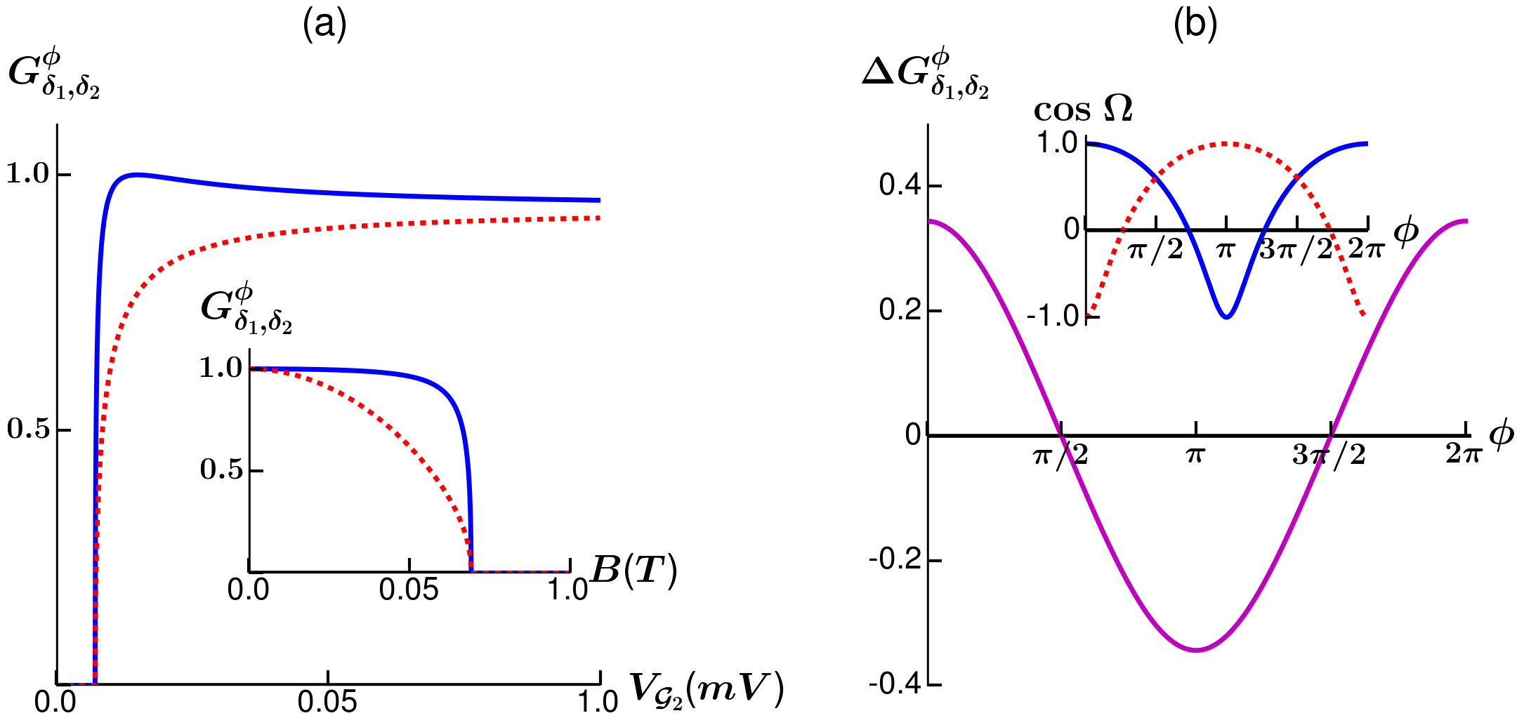
Non-topological phase for and junction dualities: Now we consider a situation where the two sides of the junction are exposed to magnetic field pointing along two different directions in the - plane (as given in Eq.2 ) which implies that the spin states associated with all momentum eigenstates belonging to the patch can be represented by points on Bloch sphere contained on a great circle lying in the - plane. While all momentum eigenstates belonging to patch will be represented on a great circle contained in the Bloch sphere lying in the - plane where . From this fact it is clear that the incident, reflected and the transmitted spinor which goes into the construction of can no longer be represented by three distinct points on the Bloch sphere which could be spotted on a single great circle. This in turn implies that half the solid angle subtended by the geodesic triangles formed by cyclic projection of these three states can never be equal to (i. e. ) and its value in general will depend on details of the position of these three states on the Bloch sphere hence rendering it non-topological or geometric (see inset of Fig.1(b) for variation of ) (also see Ref.Mehta (2009b)). Actually the angle provides an efficient handle on this geometric phase which could be tuned to be topological in two limits, i. e. for (studied above) and when all the states (incident, reflected and the transmitted spinor) once again lie on a single great circle on the Bloch sphere. The is an interesting case as it flips the signs of hence resulting in switching between type of paths and type of paths. This amounts to saying that the - junction for case is topologically equivalent to - junction for the case and similarly - junction for case is topologically equivalent to the - junction for the . Hence defines a duality (mapping between two topologically distinct junctions) between the - and - junctions and similarly between - and - junctions. Actually results in switching of two-terminal conductance between {-,-} junctions with {-, -} junctions respectively which is depicted in the plot in Fig. 1(b). This is essentially a consequence of the fact that the spin textures of the valence and conduction band gets swapped as , hence effectively converting a -doped region into a -doped region.
Proposed experimental protocol : Above we have established a topological difference between the - and - junctions. To quantify this difference in terms of experimentally measurable quantity like conductance, we consider a situation where left gate () is tuned to a n-type doping
(i. e. ) while the right gate is kept flexible so that it can be tuned to a n-type (p-type) making the system a - (-) junction by tuning the sign of () respectively. We also assume that the applied voltage bias is such that it is driving an electronic current from left to right. Owing to the symmetry of the edge spectrum about the Dirac point, the value of (see Eq.4) will be identical for a - and - junction provided we keep fixed and switch between the two types of junction only by changing the sign of while keeping its magnitude fixed.
Hence the difference in conductance (denoted by ) of a - and - junction for a given value of common to both while being different for the two junction only in sign leads to a quantity which depends linearly on the difference of (see Eq.4 ; call it ). This is so because the dependence on can be pulled out of the expression as overall scale factor. Now, note that represents that part of conductance which depends only on the spin-texture mismatch at the junction and is solely responsible for the topological classification of that junction. Hence measurement of
| (7) |
could be viewed as a quantification of the topological difference between the - and - junction. Further more, due to the duality defined earlier between - and - junction, one expects the sign of to flip keeping its magnitude fixed under under the transformation . This fact is depicted in Fig.1(b) where is plotted as a function of . Hence an experimental measurement of for and could provide a direct confirmation of the topological classification of these junctions presented in this article. Also the variation of conductance as function of strength of magnetic field- with uniform direction and a symmetric gate voltage configuration (given and opposite sign for given for - and - junction) shows asymmetry in - and - conductance which is induced by spin texture mismatch at the junction (see inset of Fig. 1(a). This asymmetry can also be seen for symmetric gate voltage configuration when conductance is plotted as a function of gate voltage while magnetic field is kept uniform and its strength is held fixed (see Fig. 1(a)).
Interaction correlation to conductance: Inclusion of electron-electron interaction on the edge leads to universal Luttinger liquid phase known for interacting 1-D electron liquidKane and Fisher (1992). As the spin Hall edge state is helical in nature the Luttinger liquid phase of such edge states lead to the helical Luttinger liquid phase Wu et al. (2006); Teo and Kane (2009); Ilan et al. (2012). Two important parameters which parametrizes the helical Luttinger liquid theory are the effective interaction parameter and the renormalized Fermi-velocity which are connected by Galilean invariance as Maslov (2005). To proceed further we first linearize the spectrum around the Fermi level which could either be in the conduction or the valence band. Then the corresponding creation operator for electrons living inside the linearized energy window could be written as
| (8) |
where are spinors evaluated at the Fermi energy for right (R) and left (L) movers and they can be imported directly from Eq.3, represents the Fermi momentum and represents slow chiral degrees of freedom which could be bosonized using standard bosonization techniquevon Delft and Schoeller (1998). Following Ref.Gangadharaiah et al., 2014 for deriving an expression for Luttinger parameter for doped helical Luttinger liquid and following Ref.Maslov, 2005 for carefully implementing the requirement of Galilean invariance, it is straight-forward to obtain the Luttinger parameter for the conduction() and valence() band as
| (9) |
where and are the Fourier transforms of screened Coulomb potential at zero and momenta. From Eq.3 it can be checked that the quantity is identical for the conduction and the valence band provided we compare situations with identical doping with respect to the zero doping situation (i. e. with respect to situation corresponding to the Fermi level lying in the middle of the gap). This fact provides a clear indication that the both for - and - junction, the effect due to electron-electron interaction are expected to be same as long the the symmetry of the spectrum about the middle of the gap stays intact.
Experimental feasibility study :
(i) Energy and length scales- A typical 2D system which hosts a helical 1D state as an edge state is the quantum spin Hall (QSH) stateHasan and Kane (2010); Qi and Zhang (2011) which was experimentally observed in HgTe/CdTe Quantum WellsKönig et al. (2008). As our proposed experiment requires application of magnetic field on the 1-D helical state which leads to breaking of TRS in general, an estimate of hierarchy of energy scales, which will protect the topological gap in the bulk but will allow for minimal breaking of TRS on the edge leading to a gapped edge spectrum is desirable. Experiments by Knig et al.König et al. (2008) reported that the QSH state is destroyed by a magnetic field of magnitude (in-plane) and (out of plane). As the SO field for the edge state point perpendicular to the plane of the 2-D quantum wells, our proposal requires application of an in plane field. Hence, an in-plane field of the order of can be considered safe as it will hardly distort the bulk QSH state but will surely open up a gap in the edge spectrum. A field amounts to gap of in the edge spectrum (if we assume a Landé-g factor of which is the g-factor for the bulk HgTe) and it further amounts to an equivalent temperature of while the experiments were done at temperatures of the order of König et al. (2008). Hence this gap can be readily resolved in present day experimental setups which makes our proposal quite feasible.
Experiment of Karmakar et al.Karmakar et al. (2011) suggests our proposal could be implemented on the QSH edge by using a nano-magnetic array.
Also, experimentally observed elastic mean free path in these edge states are Daumer et al. (2003); König et al. (2008). As our calculations were performed assuming ballistic limit, a device of length of a few micrometers could be optimal for implementing our proposal. (ii) Step function form of gate voltage and B field - As our theoretical analysis assumes a step function like variation of gate voltage and magnetic field across the - junction, it is important to understand, variation over what length scales Ojanen (2013); Klinovaja and Loss (2015) can be approximated as step function. From Eq.(1) we can idetify the length scales associated with the change in chemical potential and the magnetic field across the junction as and . When and are diagrammatically opposite but their magnitudes are same (say, ) then the factor . A linear variation of gate voltage or the which happens over length can be taken to be of step function form as far as conductance is concerned (refer supplementary material)Li et al. (2015). (iii) Symmetry of edge spectrum - Note that symmetry of the edge spectrum about its Dirac point is an important ingredient in our proposal. In general the Dirac point of edge spectrum may not lie in the middle of the bulk gap and additionally, the chemical potentials of the material may not lie at the Dirac point. Hence to implement our proposal for the - junction, the edge chemical potential should be initialized to the Dirac point by application of a global electrostatic gate. Further electrostatic gate voltages can be used with respect to this global gate voltage to tune the position of the edge chemical potential separately on the two sides of the junction.
Conclusion and outlook:
In an insightful paper by Kane and MeleKane and Mele (2005) it was shown that the quantum spin Hall phase can be classified in terms of a time reversal symmetry protected index which hosts helical edge state carrying a net equilibrium spin current. In this article we have shown that non-equilibrium charge transport (transport driven by bias) across a - junction realized on these helical edge states can also have topological classification. In our case the topology, which is directly related to helical nature of the edge spectrum, stays protected as long as the - junction is exposed to an uniaxial magnetic field. It is worth noting, in contrast to the ongoing efforts to use topology for classifying phases of condensed matter systems, in this article we present a topological classification of measurable quantities like conductance for a device element such as - junction. This view point could lead to innovative protocols for device manipulation as demonstrated in the work.
Acknowledgments: It is a pleasure to thank Jens Bardarson, Suhas Gangadharaiah for discussion, Laurens W. Molenkamp and Andrea Young for discussion and critical comments on experimental feasibility of the proposed measurement. We thank Yin-Chen-He for critical reading of the manuscript. DW would like to thank Krishnu Roy Chowdhury Santhust for helping with Python Programming. DW acknowledges University Teaching Assistantship programme offered by the University of Delhi and PM acknowledges support from the University Grants Commission under the second phase of University with Potential of Excellence at Jawaharlal Nehru University. SD acknowledges support from University of Delhi in the form of a research grant (RC/2014/6820).
References
- Berry (1984) M. V. Berry, Proc. Roy. Soc. Lond. A392, 45 (1984).
- Shapere and Wilczek (1989) A. Shapere and F. Wilczek, Geometric Phases in Physics (World Scientific, Singapore, 1989).
- Nakagawa (1987) N. Nakagawa, Ann. Phys. 179, 145 (1987).
- Aharonov and Anandan (1987) Y. Aharonov and J. Anandan, Phys. Rev. Lett. 58, 1593 (1987).
- Samuel and Bhandari (1988) J. Samuel and R. Bhandari, Phys. Rev. Lett. 60, 2339 (1988).
- Ramaseshan and Nityananda (1986) S. Ramaseshan and R. Nityananda, Curr. Sci. 55, 1225 (1986).
- Berry (1987) M. Berry, Journal of Modern Optics 34, 1401 (1987), ISSN 0950-0340.
- Pancharatnam (1956) S. Pancharatnam, Proc. Ind. Acad. Sci. A44, 247 (1956).
- Wu et al. (2006) C. Wu, B. Bernevig, and S.-C. Zhang, Phys. Rev. Lett. 96, 106401 (2006).
- Yokoyama and Murakami (2014) T. Yokoyama and S. Murakami, Physica E Low-Dimensional Systems and Nanostructures 55, 1 (2014).
- König et al. (2007) M. König, S. Wiedmann, C. Brüne, A. Roth, H. Buhmann, L. W. Molenkamp, X.-L. Qi, and S.-C. Zhang, Science (New York, N.Y.) 318, 766 (2007), ISSN 1095-9203.
- Soori et al. (2012) A. Soori, S. Das, and S. Rao, Phys. Rev. B 86, 125312 (2012).
- Mehta (2009a) P. Mehta, Phys. Rev. D 79, 096013 (2009a).
- Longuet-Higgins et al. (1958) H. C. Longuet-Higgins, U. Opik, M. H. L. Pryce, and R. A. Sack, Proc. Roy. Soc. Lond. A244, 1 (1958).
- Mehta (2009b) P. Mehta (2009b), eprint 0907.0562.
- Kane and Fisher (1992) C. L. Kane and M. P. A. Fisher, Phys. Rev. B 46, 15233 (1992).
- Teo and Kane (2009) J. C. Y. Teo and C. L. Kane, Phys. Rev. B 79, 235321 (2009).
- Ilan et al. (2012) R. Ilan, J. Cayssol, J. H. Bardarson, and J. E. Moore, Physical Review Letters 109, 216602 (2012).
- Maslov (2005) D. L. Maslov, eprint arXiv:cond-mat/0506035 (2005), eprint cond-mat/0506035.
- von Delft and Schoeller (1998) J. von Delft and H. Schoeller, Annalen der Physik 7, 225 (1998).
- Gangadharaiah et al. (2014) S. Gangadharaiah, T. L. Schmidt, and D. Loss, Phys. Rev. B 89, 035131 (2014).
- Hasan and Kane (2010) M. Z. Hasan and C. L. Kane, Rev. Mod. Phys. 82, 3045 (2010).
- Qi and Zhang (2011) X.-L. Qi and S.-C. Zhang, Rev. Mod. Phys. 83, 1057 (2011).
- König et al. (2008) M. König, H. Buhmann, L. W. Molenkamp, T. Hughes, C.-X. Liu, X.-L. Qi, and S.-C. Zhang, JPSJ 77, 031007 (2008).
- Karmakar et al. (2011) B. Karmakar, D. Venturelli, L. Chirolli, F. Taddei, V. Giovannetti, R. Fazio, S. Roddaro, G. Biasiol, L. Sorba, V. Pellegrini, et al., Physical Review Letters 107, 236804 (2011), eprint 1106.3965.
- Daumer et al. (2003) V. Daumer, I. Golombek, M. Gbordzoe, E. G. Novik, V. Hock, C. R. Becker, H. Buhmann, and L. W. Molenkamp, Applied Physics Letters p. 1376 (2003), ISSN 00036951.
- Ojanen (2013) T. Ojanen, Phys. Rev. B 87, 100506 (2013).
- Klinovaja and Loss (2015) J. Klinovaja and D. Loss, European Physical Journal B 88, 62 (2015), eprint 1408.3366.
- Li et al. (2015) T. Li, P. Wang, H. Fu, L. Du, K. A. Schreiber, X. Mu, X. Liu, G. Sullivan, G. A. Csáthy, X. Lin, et al., Phys. Rev. Lett. 115, 136804 (2015).
- Kane and Mele (2005) C. L. Kane and E. J. Mele, Physical Review Letters 95, 146802 (2005).
Supplementary Material : Numerical Calculation of Conductance
To analyse the validity of our model considered in eqn.(1) where we have assumed that both the gate voltage as well as the applied in-plane magnetic field change abruptly at the junction, we will now study a model with a junction extended over length where the applied electric and magnetic fields are connected to their assymptotic values on the two sides of the junction via a linear interpolation over a length .
We can identify length scales in our model directly from the Hamiltonian (see Eq.(1)). The length scales associated with the change in chemical potential and the magnetic field across the junction are and . When and are diagrammatically opposite assuming their magnitudes are same (say, ) then the factor . If the scale over which variation at the junction happens is shorter than the length scales and determined by the difference in assymptotic values of the chemical potential and the magnetic field respectively on the two sides of the junction then, our assumption of abrupt junction faithfully describes the situation as shown below through numerical analysis.
Now, our model with an extended junction can be divided into three regions namely, I (), II () and III (). We further divide the middle region i.e. region of extended junction into small patches such that
the Hamiltonian in the three regions can be written as -
Where, ; ;
; ; and with .
The wavefunction matching at can be expressed as -
where, is the reflection amplitude, , and are the incident and the reflected spinors respectively (see Eq.3). and are the amplitudes associated with spinors and corresponding to Hamiltonian . The spinors in the region for the case of - junction can be expressed as -
while in the case of - junction, the spinors in the region are replaced appropriately with -
with, and is the normalization constant.
In the extended junction region the wavefunction at each step is matched to wavefunction at step as -
with ; .
and are the amplitudes associated to the spinors in region II in the patch.
And, at , wavefunction matching is -
where is the transmission amplitude of the transmitted spinor as defined in eqn.(3).
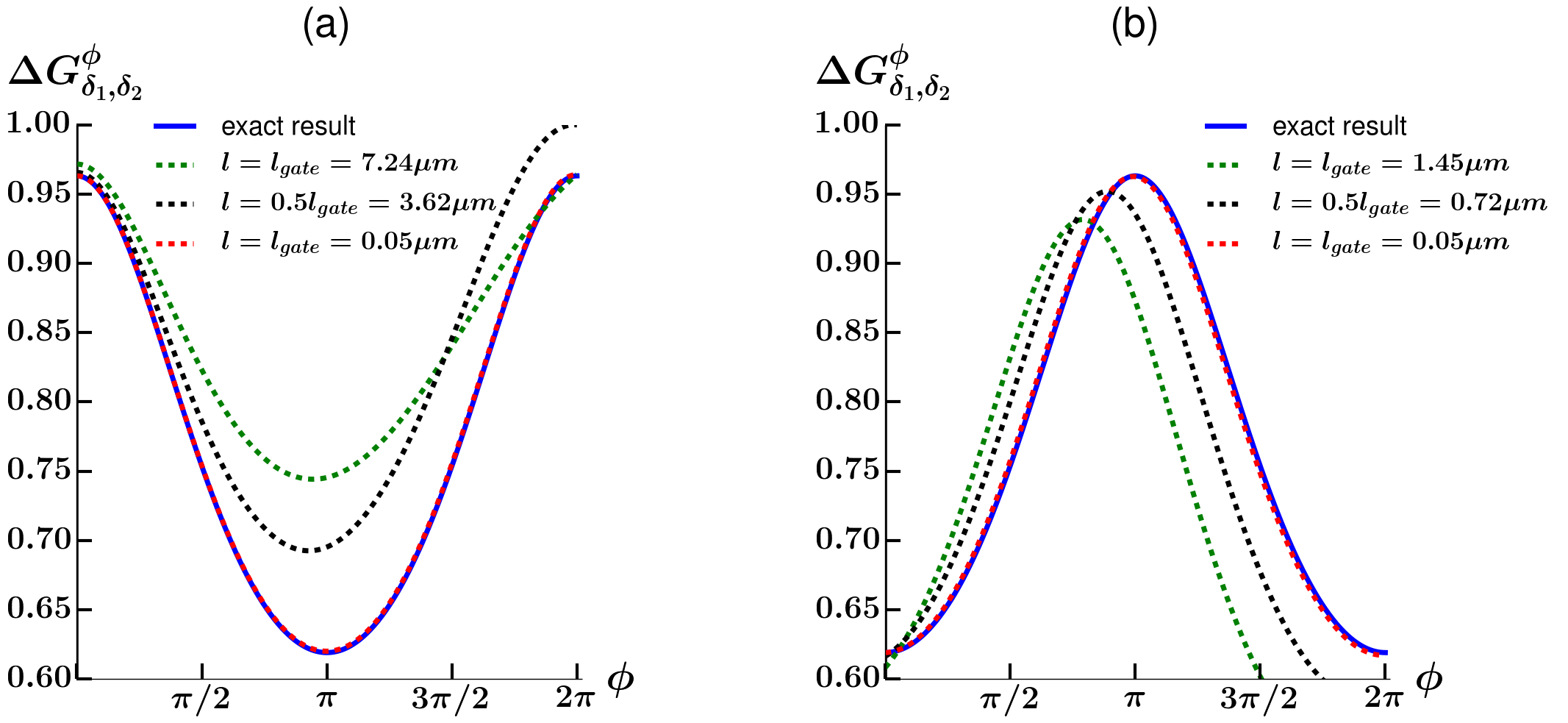
The typical value of is in case of - junction and is in case of - junction respectively while, is for both the cases as the strength of the applied magnetic field remains same in both the - and the - junctions. In fig.(3), we observe that a linear variation of gate voltage or the which happens over length can be taken to be of step function form as far as conductance is concerned. Note that for this value of , the results obtained numerically matches perfectly with the analytical results obtained in Eq.(4). This length scale seems to be feasible within the present day experimental developments.