Intrinsic disorder in graphene on transition metal dichalcogenide heterostructures
Abstract
The electronic properties of two-dimensional materials such as graphene are extremely sensitive to their environment, especially the underlying substrate. Planar van der Waals bonded substrates such as hexagonal boron nitride (hBN) have been shown to greatly improve the electrical performance of graphene devices by reducing topographic variations and charge fluctuations compared to amorphous insulating substrates Yankowitz2014 ; Dean2010 ; Xue2011 ; Decker2011 . Semiconducting transition metal dichalchogenides (TMDs) are another family of van der Waals bonded materials that have recently received interest as alternative substrates to hBN for graphene Kretinin2014 ; Larentis2014 ; Tan2014 as well as for components in novel graphene-based device heterostructures Britnell2012 ; Georgiou2013 ; Yu2013a ; Moriya2014 ; Britnell2013 ; Yu2013b ; Bertolazzi2013 ; Roy2013 . Additionally, their semiconducting nature permits dynamic gate voltage control over the interaction strength with graphene Lu2014b . Through local scanning probe measurements we find that crystalline defects intrinsic to TMDs induce scattering in graphene which results in significant degradation of the heterostructure quality, particularly compared to similar graphene on hBN devices.
Since the isolation of graphene in 2004, considerable effort has been put into finding the best substrates, both from a device standpoint and for inducing novel physical phenomena. Perhaps the most common substrate, SiO2, causes out-of-plane ripples and locally dopes the graphene due to trapped charged impurities DasSarma2011 . Suspended graphene devices, fabricated by etching away the SiO2 layer, offer the best intrinsic graphene quality, although their fabrication is far too challenging to scale to industrial levels. Hexagonal boron nitride has emerged as a very promising substrate; as an insulating crystal it not only flattens the graphene but screens underlying charge impurities from the base substrate Yankowitz2014 ; Dean2010 ; Xue2011 ; Decker2011 . Careful device fabrication techniques can yield devices of graphene quality nearing that of suspended graphene, and these heterostructures are more friendly for industrial scaling. Since hBN has a similar lattice constant to graphene, when the two lattices are in near perfect alignment interactions between the crystals strongly renormalize the graphene band structure Yankowitz2012 ; Yankowitz2014 . This opens an avenue for the study of new phenomena, such as the Hofstadter quantization, and also provides a route to make graphene insulating Yankowitz2014 . However, it may not be ideal for large scale graphene device applications where fabrication leads to a random alignment between the crystals, and the intrinsic graphene band structure needs to be preserved.
Recently, transition metal dichalcogenides have made a strong resurgence in materials research, as these crystals can be exfoliated to atomic scale thicknesses and stacked via van der Waals interactions similarly to graphene and hBN Wang2012 ; Geim2013 . A subset of the TMDs exhibit similar semiconducting behavior, with indirect band gaps in bulk ranging from 1 - 1.4 eV Wang2012 . Naïvely, these materials, when insulating, should offer comparable quality to hBN as substrates for graphene, but without the possibility of band structure modification due to their considerably different lattice constants Wilson1969 ; Lu2014b . Additionally, they offer the potential for the study of new physical phenomena (for example, potential spin-orbit coupling induced in the graphene layer due to the heavy metal atoms of the TMD Kretinin2014 ). From a device standpoint, there are numerous potential applications involving heterostructures between graphene and TMDs; for example, as tunneling transistors Britnell2012 ; Georgiou2013 ; Yu2013a ; Moriya2014 , highly efficient flexible photovoltaic devices Britnell2013 ; Yu2013b , or nonvolatile memory cells Bertolazzi2013 ; Roy2013 . Unfortunately, graphene on TMD devices have thus far been of significantly lower mobility than comparable hBN devices Kretinin2014 ; Larentis2014 ; Tan2014 , and a local understanding of this behavior is lacking. In this Letter, we show via local scanning probe measurements that graphene on TMD devices suffer an unavoidable degradation in electronic quality due to intrinsic defects in the TMD crystals.
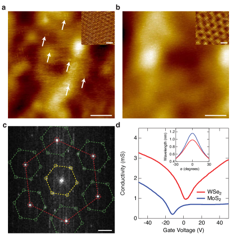
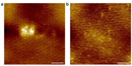
We study graphene on substrates belonging to the MX2 family, where M is a transition metal (Mo, W) and X is a chalcogen atom (S, Se, Te). The specific TMDs examined here are MoS2, WS2, WSe2, and MoTe2. We have also examined graphene on SnS2, which is not technically a TMD but shares the same crystal structure and is also a semiconductor Greenaway1965 ; Sharp2006 . Figs. 5(a) and (b) show topography images of graphene on MoS2 and WSe2 obtained via scanning tunneling microscopy (STM). Numerous defects can be observed in the MoS2 sample. The graphene lattice is continuous over these defects, indicating the defects reside in the MoS2. The strength and appearance of these defects can be tuned by the sample and gate voltages, and their appearance in other TMDs is found to depend on those factors as well as crystal thickness. The graphene on MoTe2 and SnS2 samples exhibit significantly worse topography, marked by islands of well-adhered regions surrounded by significantly rougher regions where the graphene did not appear to be adhered to the TMD, suggesting that these crystals are not stable enough in air to allow consistently good adhesion with the graphene Geim2013 (see Supplementary Information for further discussion of topography observations).
The insets of Figs. 5(a) and (b) show atomic resolution images of both samples, and additionally display hexagonal superlattices due to the interference pattern formed by the graphene and TMD lattices. As is the case for graphene on hBN, a moiré pattern is expected to form between the graphene and TMD lattices due to their relative rotation and lattice mismatch . The moiré wavelength is
where is the graphene lattice constant Yankowitz2012 . Because the lattice mismatch is much larger between graphene and TMDs than graphene and hBN, the range of possible moiré wavelengths is much smaller. The inset of Fig. 5(d) shows the dispersion of moiré wavelengths as a function of angle for graphene on MoS2 and WSe2 (the dispersions for the other TMDs studied here are very similar). The lattice constants of the TMDs in this study range from 3.15 to 3.64 Å Wilson1969 ; Greenaway1965 , and thus the possible moiré wavelengths are on the order of 0.5 nm to just over 1 nm. As a result of these short moiré wavelengths, no modification of the graphene band structure is expected at low energies Yankowitz2012 . Figure 5(c) shows a Fourier transform of the inset of Fig. 5(a), with the superlattice (yellow/green) and graphene lattice (red) hexagons highlighted.
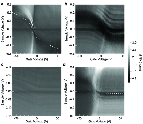
In addition to their similar crystal structure, these TMDs also share similar electronic properties. They are indirect gap semiconductors with band gaps in bulk ranging from about 1.0 eV to 1.4 eV Wang2012 (and 2.2 eV for SnS2 Sharp2006 ). In proximity to graphene, the difference in energy between the graphene work function and the electron affinity of the TMD determines the relative band alignment. The threshold gate voltage at which the TMD begins to conduct depends on this band alignment as well as the band bending related to the TMD crystal thickness Larentis2014 . For comparably thin crystals (5 - 15 nm), we observe that the Dirac point is aligned very near the conduction bands of MoS2, MoTe2 and SnS2, and closer to the middle of the gap for WS2 and WSe2. Figure 5(d) shows global conductance measurements at 4.2 K for graphene on MoS2 and WSe2. The graphene on WSe2 device is nearly symmetric around charge neutrality (indicating the WSe2 always remains insulating), whereas the MoS2 device has a saturating conductance at positive gate voltages as the MoS2 becomes conducting. We find field-effect mobilities of 5,000 - 10,000 cm2/Vs in these devices, which is over an order of magnitude lower than of comparable graphene on hBN devices. We restrict our study to thin TMD substrates as devices with thicker crystals become strongly hysteretic with gate voltage.
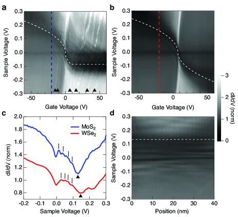
Figures 2(a) and (b) show normalized (dI/dV)/(I/V) spectroscopy measurements as a function of gate voltage for graphene on MoS2 and WSe2. For MoS2, the Dirac point (marked with a white dotted line) essentially stops moving in energy once the gate voltage is large enough to induce charge carriers in the TMD. In some samples we have additionally observed the Dirac point move with positive dVs/dVg when the MoS2 is conducting, indicative of the negative compressibility of the system Larentis2014 (see Supplementary Information). For graphene on WSe2, the Dirac point moves with the standard square root of gate voltage dispersion expected for graphene on an insulating substrate Zhang2008 , indicating the WSe2 substrate is never biased to the valence or conduction bands. In this case, the WSe2 should behave very similarly to an hBN substrate, flattening the graphene and screening charged impurities in the underlying SiO2. For all the graphene on TMD devices, the movement of the Dirac point is well fit by a Fermi velocity of 0.95 0.05 x 10⁶ m/s.
In addition to the usual spectroscopic features of graphene on an insulating substrate, we find there are extra, unexpected resonances in the dI/dV spectroscopy surrounding and moving roughly in parallel with the Dirac point. These features are ubiquitous amongst all MX2 substrates examined in this study. Fig. 2(c) shows a line cuts of Figs. 2(a) and (b) at Vg = -20 V, indicating clearly the presence of these extra states (marked with black ticks). We attribute these features to electronic scattering in graphene from point and line defects in the MX2 substrates. We have considered other origins for the extra states we observe, such as new features of the band structure due to interactions with the substrate, or the excitation of phonons in the substrate by electrons tunneling into the graphene. Such features should have well-defined energies which do not vary spatially or between different samples, depending on the exact nature of their origin. To test this hypothesis we take line maps of normalized dI/dV spectroscopy, as shown in Fig. 2(d) for graphene on MoTe2. We see clearly that the energy spacing of these states varies spatially, and in some cases the states split or merge. While this behavior is inconsistent with the alternative explanations considered above, it is consistent with extra resonances resulting from intratravalley scattering in graphene from multiple point sources.
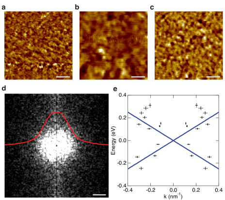
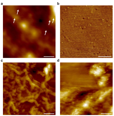
To further investigate the intravalley scattering in graphene on TMD heterostructures, we take large area dI/dV maps of graphene on WSe2 at various gate voltages (see Figs. 3(a) - (c) for three examples). The coherent features in the maps change size with gate voltage, characteristic of intravalley scattering from the Coulomb potentials of buried defects. Fig. 3(d) shows the Fourier transform of Fig. 3(c). The disk at the center of the image arises from scattering across a single graphene Dirac cone. For each map, we take a circular average of the Fourier transform and extract the corresponding wave vector as the half-width at half-maximum of the best-fit Lorentzian. These wave vectors are plotted as a function of energy relative to the Dirac point in Fig. 3(e). The resulting dispersion is in good agreement with a Fermi velocity of 0.95 x 10⁶ m/s.
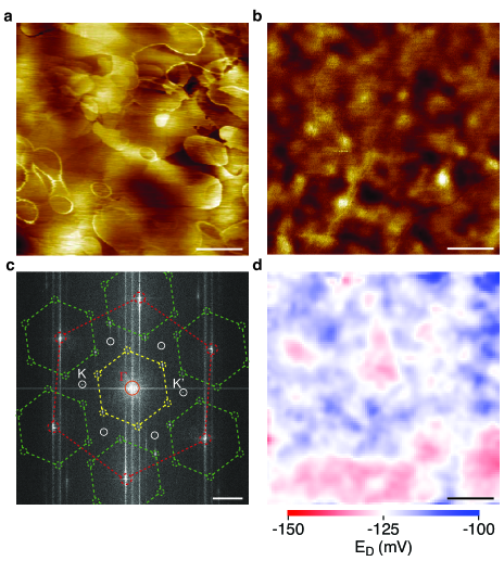
Fig. 6(a) shows a similar dI/dV map of graphene on MoS2, which exhibits numerous ring features due to the charging or discharging of defect states resulting from the hybridization of MoS2 defects with graphene (similar to those seen in artificial impurities on graphene Brar2011 ). The charging rings are the same features which run oppositely of the Dirac point in the gate map (features marked with black arrows in Fig. 2(a)). The size and nature of the rings can be tuned with back gate and sample voltage (similar ring structures have previously been observed in bare TMDs, but lacked this degree of tunability Heckl1991 ; Magonov1994 ). Of all the TMDs studied, these charging rings are unique to MoS2 (both naturally occurring and synthetic). While no ring features are observed in graphene on WSe2, there are numerous weak wandering line features which run through high resolution dI/dV maps (Fig. 6(b)). Since the graphene lattice is smooth over these line features and they are independent of sample and gate voltage, we attribute these to line dislocations intrinsic to the WSe2 crystals. Similar features are observed in graphene on WS2 as well. Fig. 6(c) shows the Fourier transform of an atomically resolved dI/dV map of graphene on MoS2. The Fourier transform exhibits the usual resonances due to the superlattice (yellow/green hexagons) and atomic lattice (yellow hexagon), as well as the long-wavelength intravalley scattering (red circle). In addition, we observe weak resonances at the K and K’ points of graphene (white circles). These resonances are indicative of intervalley scattering in graphene, which result from the presence of the atomic-scale point and line defects in the TMD substrates (for comparison, no such scattering is observed in clean graphene on hBN devices).
To address the possible influence of these defects on the charge environment in graphene, we take spatially resolved maps of the Dirac point energy (see Fig. 6(d) for graphene on WSe2). By converting the Dirac point energy to charge carrier density via , we find charge fluctuations of 1.4 0.2 x 1011 cm-2 for graphene on MoS2, WS2, and WSe2. While a few times better than the fluctuations observed in graphene on SiO2 Zhang2009 , we find these to be around an order of magnitude larger than in comparable graphene on hBN devices Xue2011 ; Decker2011 . These charge fluctuations are consistent with the defect density observed in bare MoS2 Lu2014a , suggesting that while the TMDs may be screening trapped charges in the SiO2 substrate, their own intrinsic defects still create significant static charge disorder in the graphene. Even when the bottom few layers of the MoS2 substrate are conducting and thus fully screening the SiO2 interface (i.e. at large positive gate voltages), the observed charge fluctuations are only reduced by about a factor of two, which is still considerably larger than those observed with hBN. This further implies that the fluctuations are primarily due to TMD defects (the observed reduction is likely due to enhanced screening from the conducting MoS2 layers). Finally, we do not observe any significant dependence on anneal temperature (between 150 ∘C and 300 ∘C), suggesting the defects in the TMD substrates are intrinsic to these crystals and are therefore unavoidable with current synthesis techniques.
Contrary to prior reports Lu2014b , we consistently observe a lower electronic quality of graphene on TMD devices than those using hBN. The dirtier local charge environment and prevalence of scattering is consistent with the lower mobility in our devices as well as those from prior reports Kretinin2014 ; Larentis2014 ; Tan2014 . As heterostructures of graphene and TMDs grow quickly in popularity, it is critical to understand their intrinsic limitations. Unless new methods are developed for reducing defects in TMD crystals, the quality of these heterostructures will continue to be inferior to those of graphene on hBN.
Methods
Samples are fabricated by transferring either exfoliated or CVD-grown graphene flakes onto either naturally occurring (MoS2) or synthetic (MoS2, WS2, WSe2, MoTe2, SnS2) TMD flakes. TMD flakes are exfoliated directly onto a Si substrate capped with 285 nm of thermally grown SiO2. Exfoliated graphene samples are transferred using the wet transfer technique utilized in Ref. Larentis2014 . We have not observed any difference in STM measurements between samples using exfoliated or CVD graphene, or between naturally occurring or synthetic MoS2, so these distinctions are ignored. Samples are annealed in vacuum below mbar at 300 ∘C for MoS2, WS2, and WSe2 (or 150 ∘C where otherwise noted), and 250 ∘C for MoTe2 and SnS2.
Naturally occurring bulk MoS2 crystals were purchased from SPI. Synthetic MoS2 crystals were purchased from 2D Semiconductors. WSe2 crystals were purchased from Nanoscience Instruments. 2H-WS2 crystals were grown by the direct vapor transport method of Ref. Agarwal1979 . -MoTe2 crystals were synthesized following the method of Ref. AlHilli1972 . SnS2 crystals were synthesized following the method of Ref. Sharp2006 .
All the STM measurements were performed in ultrahigh vacuum at a temperature of 4.5 K. dI/dV spectroscopy measurements were acquired by turning off the feedback circuit and adding a small (5-10 mV) a.c. voltage at 563 Hz to the sample voltage. The current was measured by lock-in detection.
Acknowledgements
The authors are thankful to Oliver Monti, David Racke, Laura Sharp, David Soltz, and Bruce Parkinson for supplying the SnS2 crystals, as well as Allan H. MacDonald for valuable theoretical discussions.
M.Y., S.H. and B.J.L. were supported by NSF Career Award No. DMR-0953784. S.L., K.K., J.X. and E.T. were supported by the Nanoelectronics Research Initiative and Intel. D.M. was supported by the NSF REU program award No. PHY-1156753.
Author contributions
M.Y. and B.J.L. performed the STM experiments. M.Y., S.L., K.K., J.X., and D.M. fabricated the devices. S.H. and B.J.L grew the CVD graphene. M.P. synthesized the bulk WS2 crystal. M.N.A. and R.J.C. synthesized the bulk MoTe2 crystal. E.T. and B.J.L. conceived and provided advice on the experiments. M.Y. and B.J.L. wrote the manuscript with input from all authors.
Supplementary Information
I Topography of Graphene on TMDs
In addition to graphene on MoS2 and WSe2, which are the focus of the main text, we have also examined graphene on WS2, MoTe2, and SnS2. Figs. 5(a), (c) and (d) show representative topography measurements of each of those samples. Graphene on WS2 is topographically similar to MoS2 and WSe2. There are visible defects, some of which are marked with black arrows in Fig. 5(a). For both graphene on MoTe2 and SnS2 we observe portions of the graphene which are well-adhered to the substrate (flat regions in Figs. 5(c) and (d)), in which a moiré pattern is clearly observed. However, the majority of the graphene region is not well-adhered to the substrate, and in these regions we are unable to observe a moiré pattern. This may indicate that the MoTe2 and SnS2 crystals are not stable enough in air to support good adhesion with graphene Geim2013 . We used the same batch of CVD graphene and transfer method as for other successful devices in this study, helping to rule out bad device fabrication as the source of this poor adhesion. Finally, we find that SnS2 completely evaporates in vacuum above 300 ∘C, further suggesting its relative instability.
II Defect Topography
For thin TMD crystals (15 nm), we only observe visible defects buried in the TMD substrates in MoS2 and WS2. However, we also observe defects in graphene on WSe2 (Fig. 5(b)) for a flake about 100 nm thick. Due to band bending of the thick WSe2 substrate Larentis2014 , the WSe2 conducts even at small positive gate voltages, whereas the thin WSe2 crystals always remain insulating for the range of gate voltages probed. One possible explanation is that the gate is able to charge defect states in the thick crystals which are not accessible in the thin crystals. This suggests that despite the lack of visible defects in the thin WSe2 samples presented in the main text, there are still localized defect states which can contribute to scattering in the graphene.
For graphene on MoS2 and WS2 where defects are visible even in thin crystals, we find we can tune the appearance of the defects with sample and gate voltages. For example, Figs. 6(a) and (b) show topography of the same 15 nm region of graphene on MoS2, taken at different sample and gate voltages. There is one large, strong defect in Fig. 6(a), but this defect is not visible in Figs. 6(b) and is instead replaced by many smaller defects in different locations. Similar behavior is observed in graphene on WS2 as well. A full classification of the exact nature of these defects is outside the scope of this work.
III Gate Maps of Graphene on TMDs
Figures 7(a) - (c) show gate maps for graphene on WS2, MoTe2 and SnS2 (similar to those shown in Figs. 2(a) and (b) of the main text for MoS2 and WSe2). For graphene on MoTe2 and SnS2, these measurements are taken in well-adhered regions of the sample, as far as possible from the adhesion boundaries. All show the presence of extra resonances surrounding the Dirac point, indicative of intravalley scattering of electrons in graphene. It is difficult to determine if the WS2 crystal becomes conducting at positive gate voltages, as the movement of the Dirac point is expected to slow as the square root of gate voltage, and the energy resolution of the Dirac point becomes worse as it moves further from the Fermi energy. Carriers may populate the WS2 as low as Vg = +20 V, but we are unable to rule out that the WS2 always remains insulating within this range of gate voltage. The white dotted lines on Fig. 7(a) represent the extremes of these two experimentally indistinguishable positions of the Dirac point (the line which stops moving with gate voltage represents the case where the WS2 becomes conducting). We were unable to obtain global transport in our graphene on WS2 device, so this method could not be used to help resolve the ambiguity. In both graphene on MoTe2 and SnS2, the movement of the Dirac point unambiguously appears to stop above small positive gate voltages.
Figure 7(d) shows a second gate map for graphene on MoS2, exhibiting considerably stronger scattering resonances than those of Fig. 2(a) of the main text. The strength of these peaks varies considerably with sample position, and the gate maps chosen for Fig. 2 of the main text exhibited weaker than usual peaks (i.e. the scattering is generally quite strong). The white dashed line at positive gate voltage marks the position of the Dirac point when the MoS2 is conducting. Since the MoS2 screens the gate, there should be no movement of the Dirac point. However, the Dirac point actually shows a slight movement towards more positive sample voltages with increasing gate voltage, which is opposite its normal movement. This positive dVs/dVg is indicative of the negative compressibility of the graphene on MoS2 heterostructure.
IV Dependence on Anneal Temperature
Ref. Kretinin2014 suggests that annealing above 150 ∘C has a degradative effect on the mobility of graphene on TMD devices. We have tested this by making graphene on MoS2, WS2, and WSe2 samples with no annealing until the heterostructure was completed, at which point the devices were annealed in vacuum at 150 ∘C. We observe qualitatively similar behavior in these devices to those annealed at higher temperatures. Specifically, these devices exhibit a similar density of visible defects, similar intravalley and intervalley scattering states, as well as similar charge fluctuations. As a final test, we further annealed the graphene on WSe2 device to 300 ∘C and observed no signatures of degradation. This is in apparent contradiction to the results of Ref. Kretinin2014 . However, as our measurements are local in nature, it is still possible that larger scale rearrangement of trapped dopants is responsible for the degradation of the device mobility.
References
- (1) Dean, C. R. et al. Boron nitride substrates for high-quality graphene electronics. Nature Nanotech. 5, 722-726 (2010).
- (2) Xue, J. et al. Scanning tunnelling microscopy and spectroscopy of ultra-flat graphene on hexagonal boron nitride. Nature Mater. 10, 282-285 (2011).
- (3) Decker, R. et al. Local Electronic Properties of Graphene on a BN Substrate via Scanning Tunneling Microscopy. Nano Lett. 11, 2291-2295 (2011).
- (4) Yankowitz, M., Xue, J., and LeRoy, B. J. Graphene on hexagonal boron nitride. J. Phys.: Condens. Matter 26 303201 (2014).
- (5) Larentis, S. et al. Band Offset and Negative Compressibility in Graphene-MoS2 Heterostructures. Nano Lett. 14, 2039-2045 (2014).
- (6) Tan, J. Y. et al. Electronic transport in graphene-based heterostructures. Appl. Phys. Lett. 104, 183504 (2014).
- (7) Kretinin, A. V. et al. Electronic Properties of Graphene Encapsulated with Different Two-Dimensional Atomic Crystals. Nano Lett. 14, 3270-3276 (2014).
- (8) Britnell, L. et al. Field-Effect Tunneling Transistor Based on Vertical Graphene Heterostructures. Science. 335 947-950 (2012).
- (9) Yu, W. J. et al. Vertically stacked multi-heterostructures of layered materials for logic transistors and complementary inverters. Nature Mater. 12, 246-252 (2013).
- (10) Georgiou, T. et al. Vertical field-effect transistor based on graphene-WS2 heterostructures for flexible and transparent electronics. Nature Nanotech. 8, 100-103 (2013).
- (11) Moriya, R. et al. Large current modulation in exfoliated-graphene/MoS2/metal vertical heterostructures. Appl. Phys. Lett. 105, 083119 (2014).
- (12) Britnell, L. et al. Strong Light-Matter Interactions in Heterostructures of Atomically Thin Films. Science. 340 1311-1314 (2013).
- (13) Yu, W. J. et al. Highly efficient gate-tunable photocurrent generation in vertical heterostructures of layered materials. Nature Nanotech. 8, 952-958 (2013).
- (14) Bertolazzi, S., Krasnozhon, D., and Kis. A. Nonvolatile Memory Cells Based on MoS2/Graphene Heterostructures. ACS Nano 7, 3246-3252 (2013).
- (15) Roy, K. et al. Graphene-MoS2 hybrid structures for multifunctional photoresponsive memory devices. Nature Nanotech. 8, 826-830 (2013).
- (16) Lu, C.-P., Li, G., Watanabe, K., Taniguchi, T., and Andrei, E. Y. MoS2: Choice Substrate for Accessing and Tuning the Electronic Properties of Graphene. Phys. Rev. Lett. 113, 156804 (2014).
- (17) Das Sarma, S., Adam, S., Hwang, E. H., and Rossi, E. Electronic transport in two-dimensional graphene. Rev. Mod. Phys. 83, 407-470 (2011).
- (18) Yankowitz, M. et al. Emergence of superlattice Dirac points in graphene on hexagonal boron nitride. Nature Phys. 8 382-386 (2012).
- (19) Wang, Q. H., Kalantar-Zadeh, K., Kis, A., Coleman, J. N., and Strano, M. S. Electronics and optoelectronics of two-dimensional transition metal dichalcogenides. Nature Nanotech. 7, 699-712 (2012).
- (20) Geim, A. K. and Grigorieva, I. V. Van der Waals heterostructures Nature 499, 419-425 (2013).
- (21) Wilson, J. A., and Yoffe, A. D. The transition metal dichalcogenides discussion and interpretation of the observed optical, electrical and structural properties. Adv. Phys. 18, 193-335 (1969).
- (22) Greenaway, D. L. and Nitsche, R. Preparation and optical properties of the group IV-VI2 chalgogenides having the CdI2 structure. J. Phys. Chem. Solids 26, 1445-1458 (1965).
- (23) Sharp, L., Soltz, D., and Parkinson, B. A. Growth and Characterization of Tin Disulfide Single Crystals. Crystal Growth & Design 6, 1523-1527 (2006).
- (24) Zhang, Y. et al. Giant phonon-induced conductance in scanning tunnelling spectroscopy of gate-tunable graphene. Nature Phys. 4, 627-630 (2008).
- (25) Brar, V. W. et al. Gate-controlled ionization and screening of cobalt adatoms on a graphene surface. Nature Phys. 7, 43-47 (2011).
- (26) Heckl, W. M., Ohnesorge, F., Binning, G., Specht, M., and Hashmi, M. Ring structures on natural molybdenum disulfide investigated by scanning tunneling and scanning force microscopy. J. Vac. Sci. Technol. B 9, 1072-1078 (1991).
- (27) Magonov, S. N., Cantow, H.-J., and Whangbo, M.-H. On the nature of nanometer-scale ring structures in the scanning tunneling microscopy images of tungsten diselenide WSe2. Surface Science 318, L1175-L1180 (1994).
- (28) Zhang, Y., Brar, V. W., Girit, C., Zettl, A., and Crommie, M. F. Origin of spatial charge inhomogeneity in graphene. Nature Phys. 5, 722-726 (2009).
- (29) Lu, C.-P., Li, G., Mao, J., Wang, L.-M., and Andrei, E. Y. Bandgap, Mid-Gap States, and Gating Effects in MoS2. Nano Lett. 14, 4628-4633 (2014).
- (30) Agarwal, M. K., Nagi Reddy, K., and Patel, H. B. Growth of tungstenite single crystals by direct vapour transport method. J. Crystal Growth 46, 139-142 (1979).
- (31) Al-Hilli, A. and Evans, B. L. The Preparation and Properties of Transition Metal Dichalcogenide Single Crystals. Journal of Crystal Growth 15, 93-101 (1972).