ACS Nano (2014)
Tiling Phosphorene
Abstract
We present a scheme to categorize the structure of different layered phosphorene allotropes by mapping their non-planar atomic structure onto a two-color 2D triangular tiling pattern. In the buckled structure of a phosphorene monolayer, we assign atoms in “top” positions to dark tiles and atoms in “bottom” positions to light tiles. Optimum bonding is maintained throughout the structure when each triangular tile is surrounded by the same number of like-colored tiles, with . Our ab initio density functional calculations indicate that both the relative stability and electronic properties depend primarily on the structural index . The proposed mapping approach may also be applied to phosphorene structures with non-hexagonal rings and 2D quasicrystals with no translational symmetry, which we predict to be nearly as stable as the hexagonal network.
keywords:
phosphorene, DFT, structure, band structure, stabilityThese authors contributed equally to this work. \altaffiliationThese authors contributed equally to this work. \abbreviationsDFT,PBE
Keywords: black phosphorus, phosphorene, DFT, ab initio, structure, band structure, stability
Phosphorene, a monolayer of black phosphorus, is emerging as a viable contender in the field of two-dimensional (2D) electronic materials.1, 2, 3 In comparison to the widely discussed semi-metallic graphene, phosphorene displays a significant band gap while still maintaining a high carrier mobility.4, 3, 5, 6 The flexible structure of semiconducting phosphorene7, 8 is advantageous in applications including gas sensing9, thermoelectrics10, and Li-ion batteries.10 Unlike flat -bonded graphene monolayers, the structure of -bonded phosphorene is buckled. There is a large number of -bonded layered phosphorene structures, including blue-P, -P, and -P,11, 12 which are nearly as stable as the related black phosphorene structure but exhibit very different electronic properties. We believe that the above list of stable phosphorene structures is still incomplete, giving rise to an unprecedented richness in terms of polymorphs and their electronic structure.

Here we introduce a scheme to categorize the structure of different layered phosphorene allotropes by mapping the non-planar 3D structure of three-fold coordinated P atoms onto a two-color 2D triangular tiling pattern. In the buckled structure of a phosphorene monolayer, we assign atoms in “top” positions to dark tiles and atoms in “bottom” positions to light tiles. Optimum bonding is maintained throughout the structure when each triangular tile is surrounded by the same number of like-colored tiles, with . Our ab initio density functional calculations indicate that both the relative stability and electronic properties depend primarily on the structural index . Common characteristics of allotropes with identical suggest the usefulness of the structural index for categorization. The proposed mapping approach may also be applied to phosphorene structures with non-hexagonal rings, counterparts of planar haeckelite,13, 14 to point and line defects,15 and to 2D quasicrystals with no translational symmetry, which we predict to be nearly as stable as the hexagonal network.
1 Results and discussion
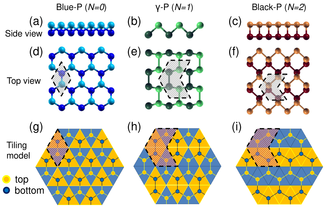
The non-planar atomic structure of selected -bonded phosphorene allotropes is depicted in side and top view in Fig. 1(a-f). We find it convenient to map the 3D structure of a phosphorene monolayer with threefold coordinated atoms onto a 2D tiling pattern by assigning a triangular tile to each atom, as shown in Fig. 1(g-i). There is a one-to-one correspondence between structures and tiling patterns, so that different structures can be distinguished by different tiling patterns. Dark-colored tiles are associated with atoms at the top and light-colored tiles with atoms at the bottom of the layer. Since each atom has 3 neighbors, each triangular tile is surrounded by 3 neighboring tiles, of which have the same color. It is obvious that provides the atom associated with the central tile with a tetrahedral neighbor coordination associated with the favorable bonding. In our tiling model, would represent the planar structure of an energetically unfavorable -bonded lattice that, according to our findings, would spontaneously convert to a non-planar -bonded allotrope.
As we will show in the following, different allotropes with , and share similar characteristics. Therefore, the structural index is useful for primary categorization of the allotropes. In each structure depicted in Fig. 1, maintains an identical value throughout the lattice, keeping the favorable bonding at all sites. We believe that this is the underlying reason for our finding that these structures are nearly equally stable.11, 12

In the first category characterized by , all neighbors of a given atom have the same, but different height within the layer, as seen in Figs. 1(a) and 1(d). This translates into a tiling pattern, where all adjacent tiles have a different color, as seen in Fig. 1(g). There is only one structural realization within the category, namely the blue-P allotrope.
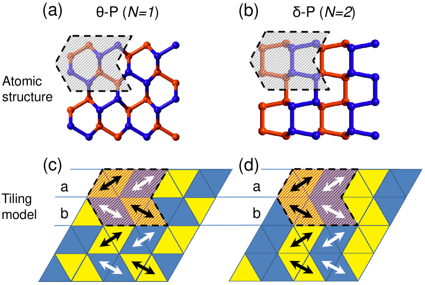
In the second category characterized by , each atom has one like neighbor at the same height and two unlike neighbors at a different height within the layer, as seen in Figs. 1(b) and 1(e). Besides the -P structure in Fig. 1(b) and 1(e), there is a -P allotrope, depicted Fig. 2(a), with the same structural index . The tiling patterns of -P and -P, shown in Figs. 1(h) and 2(c), are characterized by a diamond harlequin pattern. Each diamond, formed of two adjacent like-colored triangles, is surrounded by unlike-colored diamonds. As a guide to the eye, we indicate the orientation of the diamonds, same as the direction of the atomic bonds, by the double arrows in Fig. 2(c). The shape of the primitive unit cells shown in Figs. 1 and 2 is chosen to see more easily the correspondence between the atomic structure and the tiling pattern. The primitive unit cell of -P contains 4 atoms according to Fig. 1(h) and that of -P contains 8 atoms, as seen in Fig. 2(c). As indicated in Fig. 2(c), the orientation of diamonds in a row may be distinguished by the letters “” or “”. Whereas the perfect -P structure in Fig. 1(h) could be characterized by the sequence “” and the structure of -P by the sequence “”, an infinite number of different sequences including “” would result in an infinite number of phosphorene structures.
The most stable and best-known phosphorene allotrope is black-P, depicted in Fig. 1(c) and 1(f). Each atom in this structure has two like neighbors at the same height and one unlike neighbor at a different height, yielding a structural index . The tiling model of this structure type, shown in Fig. 1(i), contains contiguous arrays of like-colored diamonds. These arrays may be either straight, as in Fig. 1(i) for black-P, or not straight, as in Fig. 2(d) for the structurally different -P allotrope with the atomic structure shown in Fig. 2(b). Describing diamond orientation by letters “” and “” as in the case of , we may characterize black-P in Fig. 1(i) by the sequence “” and -P in Fig. 2(d) by the sequence “”. As in the case of , an infinite number of different sequences including “” would result in an infinite number of phosphorene structures.

The structural similarity and energetic near-degeneracy of and structures stems from the fact that a structural change from to involves only a horizontal shift of every other row, indicated by the horizontal lines in Figs. 2(c) and 2(d), by one tile. It is even possible to generate structural domains with different values of . The energy cost of domain wall boundaries may be extremely low12 if optimum bonding is maintained at the boundaries.
As mentioned above, there is only one allotrope with , but infinitely many structures with and . Of these, we identified and optimized all lattices with up to 28 atoms per primitive unit cell and selected other structures with up to 32 atoms per unit cell. For each lattice, we identified the relative stability with respect to the most stable black phosphorene allotrope on a per-atom basis and plotted the values in Fig. 3(a).
The electronic band structure of systems with large unit cells is very dense and hard to interpret in comparison to that of the allotropes discussed in Figs. 1 and 2, which is reproduced in the Supporting Information.16 For each of these structures, though, we identified the value of the fundamental band gap and provide the results in Fig. 3(b).
We find that neither nor display a general dependence on the size of the unit cell. We found all structures to be relatively stable. The small values eV/atom indicate a likely coexistence of different allotropes that would form under nonequilibrium conditions. All band gap values, which are typically underestimated in DFT-PBE calculations,17, 18 occur in the range between eV and eV, similar to the allotropes discussed in Figs. 1 and 2. Rather surprisingly, the distribution of and values, shown in the right panels of the sub-figures Fig. 3(a) and 3(b), exhibits three peaks that can be associated with the structural index , with a rather narrow variance caused by the differences between the allotrope structures. We find the energetically near-degenerate blue phosphorene ( with 2 atoms per unit cell) and black phosphorene ( with 4 atoms per unit cell) structures to be the most stable, followed by other structures with more than 4 atoms per unit cell. We found structures to be the least stable of all. Similarly, the blue phosphorene allotrope has the largest band gap, allotropes have the smallest band gap, and allotropes lie in between.

The higher stability of phosphorene structures in comparison to allotropes indicates an energetic preference for phosphorus atoms forming zigzag chains at the same height rather than forming isolated dimers. Among the structures, -P is the least stable, with eV/atom. All the other structures fall in-between -P and black phosphorus in terms of stability. This finding is easy to understand, since all these structures are combination of black phosphorus and -P.
For both and allotropes, we find structures with the same orientation of diamonds in the tiling pattern to be more stable. The -P structure, with all diamonds aligned in the same direction in the tiling pattern, is the most stable phosphorene allotrope, but still less stable by eV/atom than the black phosphorene. At the other extreme of the relative stability range, -P with disordered diamond orientations in the tiling pattern is the least stable allotrope, being eV/atom less stable than black phosphorene. In analogy to what we concluded for structures, all phosphorene allotropes can be viewed as a combination of -P and -P, with their stability in-between the above limiting values.
As mentioned above, also the distribution of values, shown in the right panel of Fig. 3(b), indicates three distinct groups that can be associated with the structural index . The largest band gap value of eV in the only structure, blue phosphorene, is well separated from the band gap distribution of and structures that form a double-hump shape. We note that the two peaks in the band gap distribution of and allotropes are not as well separated as the two peaks in the stability distribution in Fig. 3(a), so the trends in the band gap value are not as clear as trends in the relative stability. In systems with large unit cells, band gaps of structures are grouped around eV, whereas band gaps of structures are grouped around eV. The largest spread in values is in systems with very small unit cells. Among allotropes, we find the smallest value eV in the structure with 4 atoms/unit cell (-P) and the largest value eV in the structure with 8 atoms/unit cell (-P). Band gap values of other structures range between these two values. structures have generally the lowest band gap values of the three groups. Among systems, we find the largest value eV in the structure with 4 atoms/unit cell (black phosphorene) and eV in a system with 8 atoms/unit cell, the smallest gap value among several metastable structures of -P. Band gap values of other structures range between these two values. As discussed earlier,11, 12 our PBE-based band gap values are generally underestimated. More precise quasiparticle calculations beyond DFT, including the GW formalism, indicate that the band gap values should be about eV larger than the PBE values presented here.11, 19
As the unit cell size of and structures grows infinitely large, we gradually approach amorphous phosphorene. Assuming that our findings in Fig. 3 are universal and not limited to the finite sizes addressed by our study, we conclude that the stability and the fundamental band gap of such amorphous structures should also be found in the range suggested by their structural index .
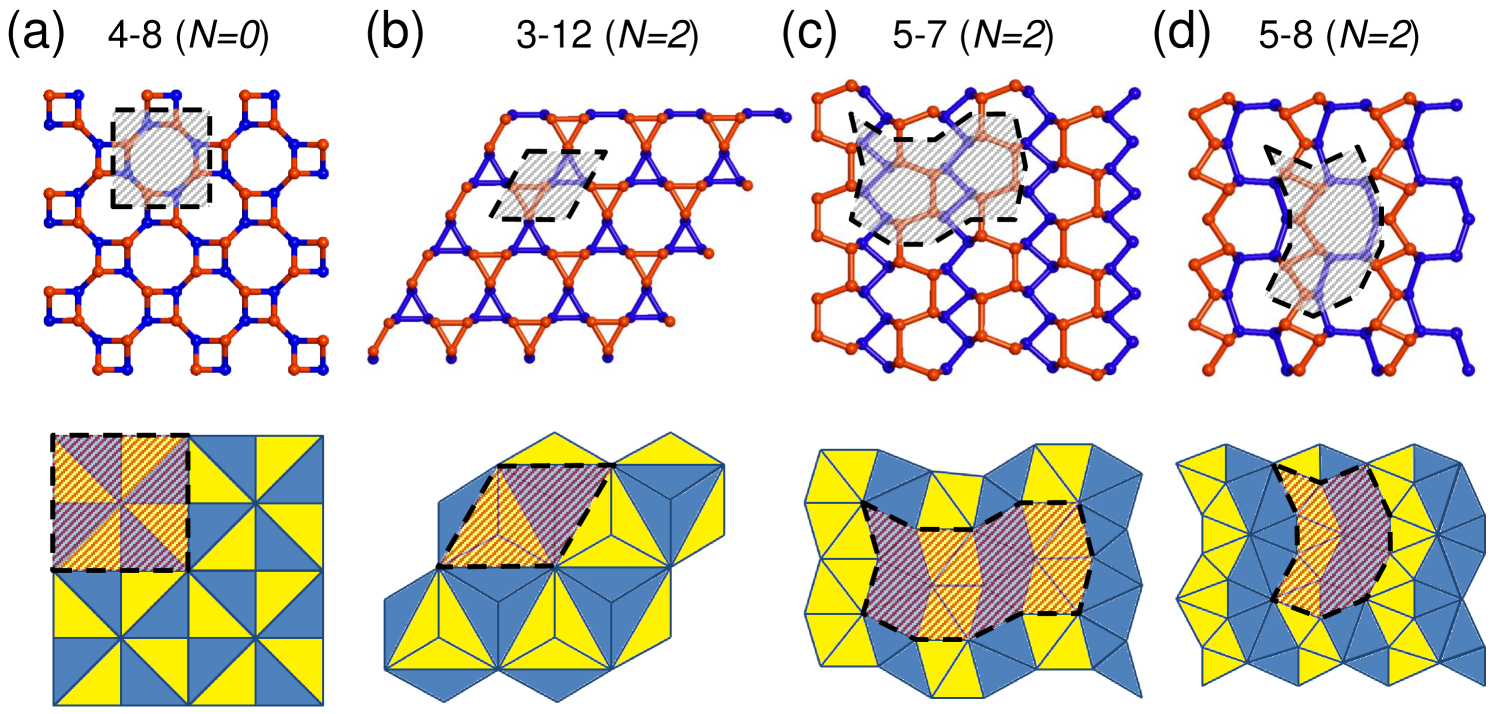
The one-to-one mapping between 3D structures of periodic systems and 2D tiling patterns is not limited to a honeycomb lattice with 6-membered rings, but can equally well be applied to lattices with , , , , and membered rings found in planar haeckelites.13, 14 The corresponding geometries and tiling patterns are shown in Fig. 4. Among these structures, 4-8 phosphorene has the highest symmetry, a relatively small unit cell with the shape of a square and a tiling pattern composed of right triangles. Besides the structure depicted in Fig. 4(a), we can identify allotropes with 4-8 rings with structural indices and . Other allotropes with 3-12, 5-7 and 5-8 rings, shown in Figs. 4(b-d), may not exist in all the variants of the structural index due to their lower symmetry. For example, the allotrope with 5-7 rings does not have a structure with .
We find structures with non-hexagonal rings to be generally less stable than the most stable black phosphorene, but the energy differences eV/atom are very small. Consequently, we expect that such structures should coexist with black phosphorene as either pure phases, or as local defects at domain wall boundaries, or as finite-size domains in the host layer. We find all phosphorene allotropes with non-hexagonal rings to be semiconducting, with the band gap determined primarily by the structural index .

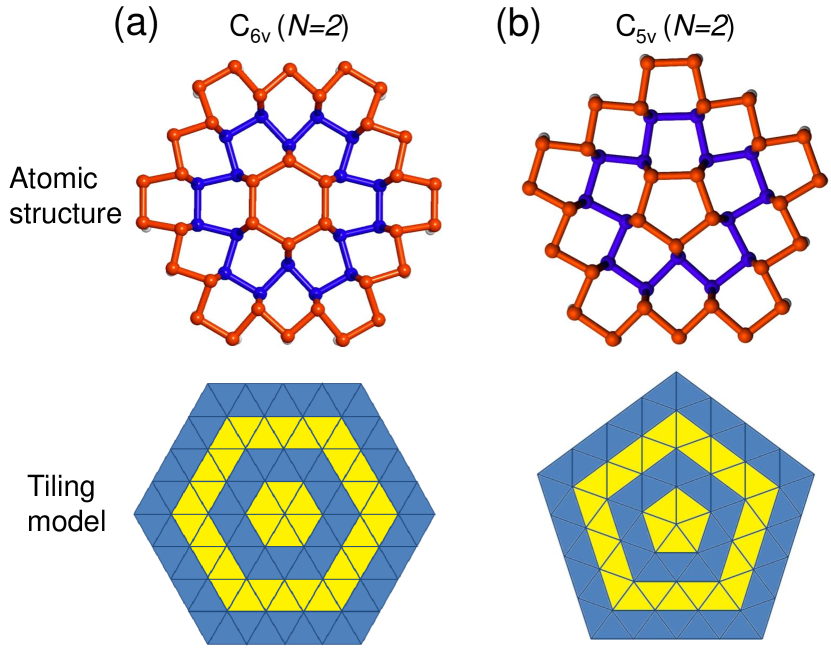
Phosphorene may also form aperiodic structures with no translational symmetry. Examples of such systems with only rotational symmetry are shown in Fig. 5. Fig. 5(a) depicts a phosphorene structure of type with a point group symmetry and the corresponding tiling pattern. In this structure, arrays of neighboring atoms form an alternating circular pattern about the center that can cover an infinite plane. The analogous structure with symmetry is depicted in Fig. 5(b), and analogous structures with symmetry could be imagined as well. To judge the stability of these aperiodic structures, we optimized finite-size flakes that were terminated by hydrogen atoms at the exposed edge. We found these structures to be semiconducting and as stable as the periodic structures discussed in Fig. 3(a), with eV/atom for the and eV/atom for the structure falling into range expected for .
These findings indicate that our classification scheme and tiling model is useful to characterize monolayers of three-fold coordinated, -hybridized phosphorus atoms arranged in periodic or aperiodic patterns. Due to structural similarities between layered structures of group-V elements, we believe that our findings regarding relative stability, electronic structure and fundamental band gap will likely also apply to other systems including monolayers of arsenic, antimony and bismuth.
Since the cohesive energy differences are rather small, we must consider the possibility that the stability ranking of the different allotropes at and related properties20 may depend on the DFT functional. We have compared PBE results for the relative stability of the different allotropes with LDA results and found the maximum difference in the relative stabilities of the different allotropes to be eV/atom, which does not change the energy ranking of the allotropes.
Since phosphorene structures will likely be synthesized at nonzero temperatures, the relative abundance of different allotropes will depend on their free energy at that temperature. Consequently, our total energy results for stability differences at need to be corrected by also addressing differences in entropy at . Even though the decrease in free energy with increasing temperature should be similar in the different allotropes due to their similar vibration spectra,11, 12, 16 minute differences in vibrational entropy may become important in view of the small differences between stabilities of the allotropes at , and could eventually change the free energy ranking at high temperatures.
In conclusion, we have introduced a scheme to categorize the structure of different layered phosphorene allotropes by mapping the non-planar 3D structure of three-fold coordinated P atoms onto a two-color 2D triangular tiling pattern. In the buckled structure of a phosphorene monolayer, we assign atoms in “top” positions to dark tiles and atoms in “bottom” positions to light tiles. We found that optimum bonding is maintained throughout the structure when each triangular tile is surrounded by the same number of like-colored tiles, with . Our ab initio density functional calculations indicate that both the relative stability and electronic properties depend primarily on the structural index . Common characteristics of allotropes with identical suggest the usefulness of the structural index for categorization. The proposed mapping approach may also be applied to phosphorene structures with non-hexagonal rings and to 2D quasicrystals with no translational symmetry, which we predict to be nearly as stable as the hexagonal network.
2 Methods
Our computational approach to gain insight into the equilibrium structure, stability and electronic properties of various phosphorene structures is based on ab initio density functional theory (DFT) as implemented in the SIESTA17. We used periodic boundary conditions throughout the study. We used the Perdew-Burke-Ernzerhof (PBE)18 exchange-correlation functional, norm-conserving Troullier-Martins pseudopotentials21, and a double- basis including polarization orbitals. Selected PBE results were compared to results based on the Local Density Approximation (LDA) 22, 23. The reciprocal space was sampled by a fine grid24 of -points in the Brillouin zone of the primitive unit cell. We used a mesh cutoff energy of Ry to determine the self-consistent charge density, which provided us with a precision in total energy of 2 meV/atom. All geometries have been optimized by SIESTA using the conjugate gradient method25, until none of the residual Hellmann-Feynman forces exceeded eV/Å.
We thank Luke Shulenburger for useful discussions. This study was supported by the National Science Foundation Cooperative Agreement #EEC-0832785, titled “NSEC: Center for High-rate Nanomanufacturing”. Computational resources have been provided by the Michigan State University High Performance Computing Center. shown in this document.
References
- Narita et al. 1983 Narita, S.; Akahama, Y.; Tsukiyama, Y.; Muro, K.; Mori, S.; Endo, S.; Taniguchi, M.; Seki, M.; Suga, S.; Mikuni, A. et al. Electrical and Optical Properties of Black Phosphorus Single Crystals. Physica B+C 1983, 117&118, 422–424
- Maruyama et al. 1981 Maruyama, Y.; Suzuki, S.; Kobayashi, K.; Tanuma, S. Synthesis and Some Properties of Black Phosphorus Single Crystals. Physica B+C 1981, 105, 99–102
- Liu et al. 2014 Liu, H.; Neal, A. T.; Zhu, Z.; Luo, Z.; Xu, X.; Tomanek, D.; Ye, P. D. Phosphorene: An Unexplored 2D Semiconductor with a High Hole Mobility. ACS Nano 2014, 8, 4033–4041
- Li et al. 2014 Li, L.; Yu, Y.; Ye, G. J.; Ge, Q.; Ou, X.; Wu, H.; Feng, D.; Chen, X. H.; Zhang, Y. Black phosphorus field-effect transistors. Nature Nanotech. 2014, 9, 372–377
- Koenig et al. 2014 Koenig, S. P.; Doganov, R. A.; Schmidt, H.; Castro Neto, A. H.; Özyilmaz, B. Electric Field Effect in Ultrathin Black Phosphorus. Appl. Phys. Lett. 2014, 104, 103106
- Xia et al. 2014 Xia, F.; Wang, H.; Jia, Y. Rediscovering Black Phosphorus: A Unique Anisotropic 2D Material for Optoelectronics and Electronics. Nature Commun. 2014, 5, 4458
- Fei and Yang 2014 Fei, R.; Yang, L. Strain-Engineering the Anisotropic Electrical Conductance of Few-Layer Black Phosphorus. Nano Lett. 2014, 14, 2884–2889
- Rodin et al. 2014 Rodin, A. S.; Carvalho, A.; Castro Neto, A. H. Strain-Induced Gap Modification in Black Phosphorus. Phys. Rev. Lett. 2014, 112, 176801
- Kou et al. 2014 Kou, L.; Frauenheim, T.; Chen, C. Phosphorene as a Superior Gas Sensor: Selective Adsorption and Distinct I-V Response. J. Phys. Chem. Lett. 2014, 5, 2675–2681
- Fei et al. 2014 Fei, R.; Faghaninia, A.; Soklaski, R.; Yan, J.-A.; Lo, C.; Yang, L. Enhanced Thermoelectric Efficiency via Orthogonal Electrical and Thermal Conductances in Phosphorene. Nano Lett. 2014, 14, 6393–6399
- Zhu and Tománek 2014 Zhu, Z.; Tománek, D. Semiconducting Layered Blue Phosphorus: A Computational Study. Phys. Rev. Lett. 2014, 112, 176802
- Guan et al. 2014 Guan, J.; Zhu, Z.; Tománek, D. Phase Coexistence and Metal-Insulator Transition in Few-Layer Phosphorene: A Computational Study. Phys. Rev. Lett. 2014, 113, 046804
- Fthenakis et al. 2014 Fthenakis, Z. G.; Zhu, Z.; Tománek, D. Effect of Structural Defects on the Thermal Conductivity of Graphene: From Point to Line Defects to Haeckelites. Phys. Rev. B 2014, 89, 125421
- Terrones et al. 2000 Terrones, H.; Terrones, M.; Hernández, E.; Grobert, N.; Charlier, J.-C.; Ajayan, P. M. New Metallic Allotropes of Planar and Tubular Carbon. Phys. Rev. Lett. 2000, 84, 1716–1719
- Liu et al. 2014 Liu, Y.; Xu, F.; Zhang, Z.; Penev, E. S.; Yakobson, B. I. Two-Dimensional Mono-Elemental Semiconductor with Electronically Inactive Defects: The Case of Phosphorus. Nano Lett. 2014, doi:10.1021/nl5021393
- 16 See the Supporting Information for the electronic band structure of the phosphorene allotropes discussed in Figs. 1 and 2 and the phonon band structure of -P.
- Artacho et al. 2008 Artacho, E.; Anglada, E.; Dieguez, O.; Gale, J. D.; Garcia, A.; Junquera, J.; Martin, R. M.; Ordejon, P.; Pruneda, J. M.; Sanchez-Portal, D. et al. The SIESTA Method; Developments and Applicability. J. Phys. Cond. Mat. 2008, 20, 064208
- Perdew et al. 1996 Perdew, J. P.; Burke, K.; Ernzerhof, M. Generalized Gradient Approximation Made Simple. Phys. Rev. Lett. 1996, 77, 3865–3868
- Tran et al. 2014 Tran, V.; Soklaski, R.; Liang, Y.; Yang, L. Layer-Controlled Band Gap and Anisotropic Excitons in Few-Layer Black Phosphorus. Phys. Rev. B 2014, 89, 235319
- Han et al. 2014 Han, X.; Stewart, H. M.; Shevlin, S. A.; Catlow, C. R. A.; Guo, Z. X. Strain and Orientation Modulated Bandgaps and Effective Masses of Phosphorene Nanoribbons. Nano Lett. 2014, 14, 4607–4614
- Troullier and Martins 1991 Troullier, N.; Martins, J. L. Efficient Pseudopotentials for Plane-Wave Calculations. Phys. Rev. B 1991, 43, 1993
- Ceperley and Alder 1980 Ceperley, D. M.; Alder, B. J. Ground State of the Electron Gas by a Stochastic Method. Phys. Rev. Lett. 1980, 45, 566–569
- Perdew and Zunger 1981 Perdew, J. P.; Zunger, A. Self-interaction correction to density-functional approximations for many-electron systems. Phys. Rev. B 1981, 23, 5048–5079
- Monkhorst and Pack 1976 Monkhorst, H. J.; Pack, J. D. Special Points for Brillouin-Zone Integrations. Phys. Rev. B 1976, 13, 5188–5192
- Hestenes and Stiefel 1952 Hestenes, M. R.; Stiefel, E. Methods of Conjugate Gradients for Solving Linear Systems. J. Res. Natl. Bur. Stand. 1952, 49, 409–436