Hard Gap in Epitaxial Semiconductor-Superconductor Nanowires
Many present and future applications of superconductivity would benefit from electrostatic control of carrier density and tunneling rates, the hallmark of semiconductor devices. One particularly exciting application is the realization of topological superconductivity Kitaev as a basis for quantum information processing DasSarmaTopoComp ; JasonAliceaTopoComp . Proposals in this direction based on proximity effect in semiconductor nanowires are appealing because the key ingredients are currently in hand DasSarmaMajorana1D ; VonOppenMajorana1D . However, previous instances of proximitized semiconductors show significant tunneling conductance below the superconducting gap, suggesting a continuum of subgap states—a situation that nullifies topological protection DasSarmaTopoProtection ; DanielLossPoisoning . Here, we report a hard superconducting gap induced by proximity effect in a semiconductor, using epitaxial Al-InAs superconductor-semiconductor nanowires. The hard gap, along with favorable material properties and gate-tunability, makes this new hybrid system attractive for a number of applications, as well as fundamental studies of mesoscopic superconductivity.
Key signatures of topological superconductivity, including a characteristic zero-bias tunneling peak appearing at finite magnetic field, have been reported by several groups over the past few years LeoMajorana ; MotyMajorana ; MingtangMajorana ; HughMajorana . In all cases, a soft gap is also seen, indicated by sizable subgap conductance. The origin of the soft gap is not fully understood, with recent theory attributing it to disorder at the semiconductor/superconductor interface DasSarmaSoftGap . Besides complicating an already complex mesoscopic system by allowing alternative (Kondo) processes that themselves can give rise to zero-bias tunneling peaks, subgap states are fatal to topological protection. This is because quasiparticles occupying subgap states will inadvertently participate in braiding, thus influencing resulting quantum states in an unpredictable and possibly time-dependent way DasSarmaTopoProtection ; DanielLossPoisoning .
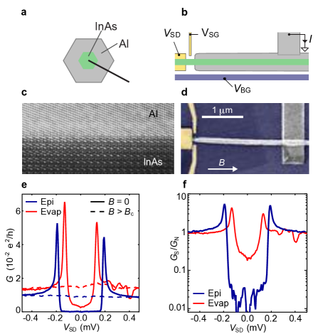
InAs nanowires were grown in the wurtzite [0001] direction by molecular beam epitaxy (MBE) using gold nanoparticles as catalysts PeterInAs . After the nanowires reached a length of 5–10 m, Al was grown at low temperature by angled deposition within the MBE chamber. The resulting semiconductor-superconductor interface, shown in Fig. 1c, appears coherent, domain matched, and impurity free. Material growth is described in detail in Ref. KrogstrupGrowth . Rotating the substrate during Al growth results in full-shell nanowires with epitaxial interfaces on all facets (Fig. 1a); directional growth without rotating yields half-shell nanowires, with epitaxial Al on two or three facets of the hexagonal InAs core (Fig. 5a). The nanowires were dispersed onto a doped Si substrate with a 100 nm oxide. The Al shell was contacted by superconducting Ti/Al (5/130 nm) and the InAs core (exposed with a selective Al etch) with normal Ti/Au (5/80 nm). Modest in situ ion milling was used to improve contact between both the core and shell to leads. A device similar to the one measured is shown in Fig. 1d. Control devices were fabricated by etching away the Al shell and evaporating Ti/Al in select areas (Figs. 1b and 1d). (The 5 nm Ti sticking layer improved gap hardness in all control devices. See supplementary information).
Measurements were carried out in a dilution refrigerator with a base temperature of 20 mK. Carrier density in the exposed InAs was tuned via the backgate voltage, ; the side gate was not used in these measurements. External magnetic field, , was applied along the nanowire axis, unless stated otherwise. Seven epitaxial devices (along with eight control devices) have been measured to date and show similar behavior.
Tunneling spectra of a full-shell epitaxial device and an evaporated control device in the weak tunneling regime, with conductance of the exposed core tuned to , are shown in Fig. 1e. In the superconducting state (), differential conductance as a function of source-drain voltage, , showed strongly suppressed conductance between symmetric peaks. Above a critical value of field, (75 mT for epitaxial, 250 mT for control), both devices showed featureless normal-state tunneling conductances, , of . Ratios for the epitaxial and control devices are shown in Fig. 1f. The positions of the peaks in indicate an induced gap of 190 eV, similar to the gap of bulk Al. Figure 1f shows the subgap conductance suppressed by a factor of relative to either normal state () or above-gap conductance. The evaporated control device shows a slightly smaller induced gap of 140 eV, and a suppression of subgap conduction by a factor up to , comparable to previous measurements in proximitized InAs and InSb nanowires LeoMajorana ; MotyMajorana ; MingtangMajorana ; HughMajorana ; WillyABS ; FinckMajorana .
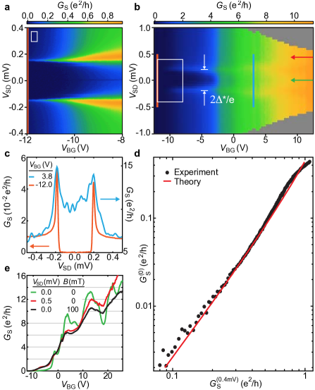
Increasing in the full-shell device increased both subgap and above-gap conductance (Fig. 2). Conductance peaks at 190 V, indicating the induced gap, did not depend on gate voltage. At positive gate voltages (more open barrier), subgap conductance exceeds the corresponding normal state conductance, as expected for a moderate-transmission barrier BTK ; BeenakkerNSJunction . Enhanced subgap conductance is evident in Fig. 2c, which shows two vertical cuts taken at low and high backgate voltages (orange and blue lines in Figs. 2a and 2b). In Fig. 2d, the superconducting zero-bias conductance is plotted as a function of above-gap conductance ( 0.4 mV) along with theoretical dependence of on BeenakkerNSJunction
| (1) |
with no fit parameters. Using the high-bias conductance ( 0.4 mV ) in place of the normal state conductance is justified by their observed equality in the experiment (see Fig. 1f). Agreement between experiment and the one-channel limit of theory BeenakkerNSJunction over a broad range of conductances indicates that transmission in the constriction is single channel.
The device reported in Fig. 2 exhibited conductance steps as a function of (Fig. 2e), a typical signature of quantum point contacts (QPC). Zero-bias conductance in the normal state (black line) shows plateaus at values close to 1, 3, 6, and 10 . These unconventional quantization values could be attributed to imperfect transmission of one-dimensional conduction modes ballisticInAs or symmetries in the transverse confining potential of the nanowire unevenQPC . In addition, while we have subtracted line resistances from our measurement set-up, we cannot independently determine contact resistances within the device, which affect plateau values. In the superconducting state and at source-drain bias above (red line), the device conductance shows a similar behavior, but begins to deviate above 6 . Plateaus are less well defined at zero-bias in the superconducting state (green line). Instead, conductance oscillates around the normal state values and peaks on the lower edge of the normal state plateaus.
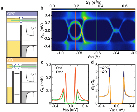
In some devices, both epitaxial and evaporated, the exposed core region forms a quantum dot (QD) rather than a QPC (Fig. 3a). The formation of a QD versus a QPC barrier depend on the length of the exposed wire, as indicated in Fig. 3(a), but is not yet under full experimental control. In the normal state of an epitaxial full-shell device with a QD barrier, Coulomb blockade diamonds and Kondo related even-odd structures can be identified (see supplementary information). Since the charging energy of the reported QD device is larger than the induced gap , when is tuned to the middle of an even Coulomb diamond, the discrete QD states are far from the edge of the induced gap. The QD thus acts as a single tunnel barrier between the normal lead and the proximitized InAs core. Accordingly, tunneling spectra for QPC and even-valley QD devices were found to be essentially identical (Fig. 3d).
In odd-occupied Coulomb valleys, symmetric subgap resonances (SGRs) were observed, forming a characteristic eye shape (Fig. 3b). These SGRs, arising from Andreev bound states or Yu-Shiba-Rusinov states Yu ; Shiba ; Rusinov , crossed due to Coulomb interaction, have been previously investigated experimentally and theoretically SeigoABS ; SilvanoSpinSplit ; WillyABS ; NadyaMasonABS ; PilletABS ; TobiasMengABS ; SeigoKondoABS ; YeyatiABS . Similar QD structure and their associated SGRs in the superconducting state are also observed in the evaporated-Al control devices. Vertical cuts at the particle-hole symmetry point of an odd (orange) and even (green) Coulomb valley are shown in Fig. 3c.
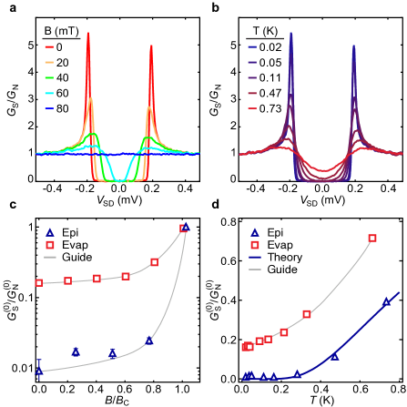
Figure 4 shows the evolution of the proximity-induced gap as a function of magnetic field and temperature. We compare the normalized zero-bias conductance of an epitaxial full-shell device against an evaporated control device in Figs. 4c and 4d. Since the subgap conductance in epitaxial devices is close to our experimental noise-floor, we average over a 40 V window centered about zero-bias and define this value as . For better comparison, we normalize the applied magnetic field by the critical fields of each device in Fig. 4c. Fig. 4d shows the normalized zero-bias conductance as a function of temperature. Temperature dependence of tunneling conductance of a N-S junction is given by the expression tinkham
| (2) |
where is the Boltzmann constant and is the temperature. From the theoretical fit, we extract an induced gap of 160 eV, close to, but not identical to the 190 eV measured directly from tunneling spectroscopy. We note in Fig. 4a and 4c that the floor of the induced gap in the epitaxial devices remains close to zero conductance, rising sharply only when approaches . Retaining a hard gap at finite magnetic fields is important for potential applications in topological quantum computing. We do not know of a theoretical treatment of this dependence to which we can compare the data.
Devices with half-shell nanowires were fabricated by identical methods, though with two superconducting Al leads instead of one, both leads contacting the Al half-shell and the InAs core on the uncovered side of the nanowire (Fig. 5). Tunneling spectroscopy on these devices also shows very low subgap conductance and a gap of 180 eV (Fig. 5c), slightly smaller than the induced gap in the full-shell devices. Subgap conductance is a factor of below the normal state or high-bias conductance, significantly better than in the evaporated control devices, but not quite as low as the full-shell device for reasons that are not yet understood.
Using two superconducting leads in the half-shell device allowed us to measure the conductance of the nanowire while the electron density in the half-exposed InAs core is tuned via a side or back gate. As illustrated in Fig. 5b, conductance across the two Al leads was measured in a current biased configuration with the device in the normal state ( 100 mT ). Conductance remained roughly constant at 10 below V, then rose to 45 at more positive (Fig. 5e). We interpret the saturated conductance at negative gate voltages to be the conductance of the Al shell, and the subsequent increase in conductance at positive gate voltages as due to a parallel conduction channel through the InAs core. Using the capacitance model from Ref. CapacitanceModel , we estimate the following transport parameters for the InAs core: carrier density (at high ), ; mobility, ; elastic scattering length, . These are typical values for InAs nanowires reported in Refs. LeoSInAsS ; ThomasInAs . However, the expected resistance for our Al shell should be on the order of . The higher measured resistance could be attributed to additional contact resistance between the Al leads and the Al shell, or disorder in the Al shell for this particular sample. Regardless of series resistance, the observed saturation of conductance at the negative end of the gate voltage range suggests that the wire is fully depleted at that point. Future experiments with multiple side gates will improve control of density along the wire.
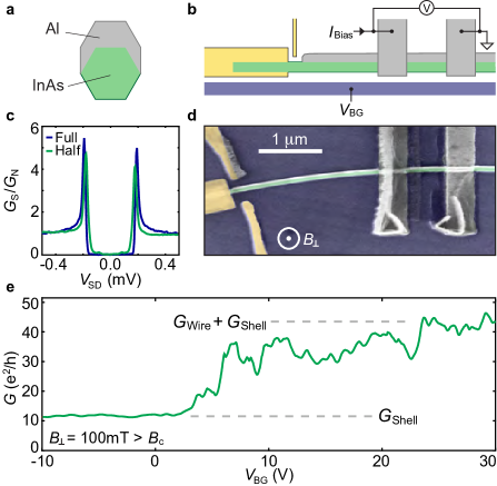
While the full-shell nanowires provide fully protective coating as well as an interesting geometry—a cylindrical superconductor—it is presumably the half-shell devices that are of more direct applicability to topological superconductivity and Majorana devices. The possibility of controlling the subband occupation in a large spin-orbit, large g-factor quasi-one-dimensional semiconductor, while maintaining a hard induced superconducting gap, makes the epitaxial half-shell nanowire an ideal platform for nanowire-based Majorana devices and many other applications.
We thank E. Johnson for electron microscopy and K. Flensberg for valuable discussions. Research supported by Microsoft Project Q, the Danish National Research Foundation, the Carlsberg Foundation, the Villum Foundation, the Lundbeck Foundation, and the European Commission.
References
- (1) Kitaev, A. Y. Unpaired majorana fermions in quantum wires. Phys.-Usp. 44, 131 (2001).
- (2) Nayak, C., Simon, S. H., Stern, A., Freedman, M. & Das Sarma, S. Non-abelian anyons and topological quantum computation. Rev. Mod. Phys. 80, 1083–1159 (2008).
- (3) Alicea, J., Oreg, Y., Refael, G., von Oppen, F. & Fisher, M. P. A. Non-abelian statistics and topological quantum information processing in 1d wire networks. Nature Phys. 7, 412–417 (2011).
- (4) Lutchyn, R. M., Sau, J. D. & Das Sarma, S. Majorana fermions and a topological phase transition in semiconductor-superconductor heterostructures. Phys. Rev. Lett. 105, 077001 (2010).
- (5) Oreg, Y., Refael, G. & von Oppen, F. Helical liquids and majorana bound states in quantum wires. Phys. Rev. Lett. 105, 177002 (2010).
- (6) Cheng, M., Lutchyn, R. M. & Das Sarma, S. Topological protection of majorana qubits. Phys. Rev. B 85, 165124 (2012).
- (7) Rainis, D. & Loss, D. Majorana qubit decoherence by quasiparticle poisoning. Phys. Rev. B 85, 174533 (2012).
- (8) Mourik, V. et al. Signatures of majorana fermions in hybrid superconductor-semiconductor nanowire devices. Science 336, 1003–1007 (2012).
- (9) Das, A. et al. Zero-bias peaks and splitting in an Al-InAs nanowire topological superconductor as a signature of majorana fermions. Nature Phys. 8, 887–895 (2012).
- (10) Deng, M. T. et al. Anomalous zero-bias conductance peak in a Nb-InSb nanowire-Nb hybrid device. Nano Lett. 12, 6414–6419 (2012).
- (11) Churchill, H. O. H. et al. Superconductor-nanowire devices from tunneling to the multichannel regime: Zero-bias oscillations and magnetoconductance crossover. Phys. Rev. B 87, 241401 (2013).
- (12) Takei, S., Fregoso, B. M., Hui, H.-Y., Lobos, A. M. & Das Sarma, S. Soft superconducting gap in semiconductor majorana nanowires. Phys. Rev. Lett. 110, 186803 (2013).
- (13) Krogstrup, P. et al. Junctions in axial III-V heterostructure nanowires obtained via an interchange of group III elements. Nano Letters 9, 3689–3693 (2009). PMID: 19842690.
- (14) Krogstrup, P. et al. Semiconductor-superconductor nanowire epitaxy. submitted (2014).
- (15) Chang, W., Manucharyan, V. E., Jespersen, T. S., Nygård, J. & Marcus, C. M. Tunneling spectroscopy of quasiparticle bound states in a spinful josephson junction. Phys. Rev. Lett. 110, 217005 (2013).
- (16) Finck, A. D. K., Van Harlingen, D. J., Mohseni, P. K., Jung, K. & Li, X. Anomalous modulation of a zero-bias peak in a hybrid nanowire-superconductor device. Phys. Rev. Lett. 110, 126406 (2013).
- (17) Beenakker, C. W. J. Quantum transport in semiconductor-superconductor microjunctions. Phys. Rev. B 46, 12841–12844 (1992).
- (18) Blonder, G. E., Tinkham, M. & Klapwijk, T. M. Transition from metallic to tunneling regimes in superconducting microconstrictions: Excess current, charge imbalance, and supercurrent conversion. Phys. Rev. B 25, 4515–4532 (1982).
- (19) Chuang, S. et al. Ballistic InAs nanowire transistors. Nano Lett. 13, 555–558 (2013).
- (20) Ford, A. C., Kumar, S. B., Kapadia, R., Guo, J. & Javey, A. Observation of degenerate one-dimensional sub-bands in cylindrical InAs nanowires. Nano Lett. 12, 1340–1343 (2012).
- (21) Yu, L. Bound state in superconductors with paramagnetic impurities. Acta Phys. Sin. 21, 75 (1965).
- (22) Shiba, H. Classical spins in superconductors. Prog. Theor. Phys. 40, 435–451 (1968).
- (23) Rusinov, A. I. Theory of gapless superconductivity in alloys containing paramagnetic impurities. Sov. Phys. JETP 29, 1101–1106 (1969).
- (24) Deacon, R. S. et al. Tunneling spectroscopy of andreev energy levels in a quantum dot coupled to a superconductor. Phys. Rev. Lett. 104, 076805 (2010).
- (25) Lee, E. J. H. et al. Spin-resolved andreev levels and parity crossings in hybrid superconductor-semiconductor nanostructures. Nature Nanotechnol. 9, 79–84 (2014).
- (26) Dirks, T. et al. Transport through andreev bound states in a graphene quantum dot. Nature Phys. 7, 386–390 (2011).
- (27) Pillet, J.-D. et al. Andreev bound states in supercurrent-carrying carbon nanotubes revealed. Nature Phys. 6, 965–969 (2010).
- (28) Meng, T., Florens, S. & Simon, P. Self-consistent description of andreev bound states in josephson quantum dot devices. Phys. Rev. B 79, 224521 (2009).
- (29) Deacon, R. S. et al. Kondo-enhanced andreev transport in single self-assembled InAs quantum dots contacted with normal and superconducting leads. Phys. Rev. B 81, 121308 (2010).
- (30) Vecino, E., Martín-Rodero, A. & Yeyati, A. L. Josephson current through a correlated quantum level: andreev states and junction behavior. Phys. Rev. B 68, 035105 (2003).
- (31) Tinkham, M. Introduction to Superconductivity: Second Edition. Dover Books on Physics (Dover Publications, 2004).
- (32) Wunnicke, O. Gate capacitance of back-gated nanowire field-effect transistors. Appl. Phys. Lett. 89, 083102 (2006).
- (33) Doh, Y.-J. et al. Tunable supercurrent through semiconductor nanowires. Science 309, 272–275 (2005).
- (34) Jespersen, T. S., Polianski, M. L., Sørensen, C. B., Flensberg, K. & Nygård, J. Mesoscopic conductance fluctuations in InAs nanowire-based SNS junctions. New J. Phys. 11, 113025 (2009).
I Supplementary Information for “Hard Gap in Epitaxial Superconductor-Semiconductor Nanowires“”
I.1 Additional information on device fabrication
We sonicated the growth substrate in methanol to liberate the epitaxially grown nanowires. Droplets of the nanowire suspension were then deposited on target substrates and allowed to dry. Nanowires were then optically located relative to pre-fabricated alignment marks. Finally we patterned electrodes onto the substrate with standard electron-beam lithography techniques.
Aluminum Etchant - Type D, manufactured by Transene Company Inc., was used to remove the Al shell from the InAs core.
Native oxides, both on the Al shell and the exposed InAs core, were removed with Ar ion-milling. This was performed in the same chamber as the electron-beam evaporator used for metals deposition.
I.2 Control devices
I.2.1 Without Ti sticking layer
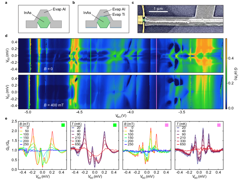
Epitaxial half-shell nanowires from the same growth were used for both the epitaxial half-shell devices and the evaporated control devices. For the control, all of the native Al shell was chemically removed. Al, or Ti/Al (Ti being the sticking layer), was then evaporated onto the remnant InAs core to create a final device similar to the one shown in Supplementary Fig. 1c. Supplementary Figs. 1a and 1b illustrate the cross-sectional profile of these control devices.
In this section we focus only on evaporated control devices without a Ti sticking layer. Supplementary Fig. 1d shows the differential conductance of a control device as a function of and . The lower panel shows data from the same region in , but taken at 400 mT . The device appears to be highly switchy as the tunneling spectrum is discontinuous in . We can see faint suggestions of Coulomb diamond structures, but the lack of a clear even-odd structure tells us that there are potentially multiple ill-defined QDs in the InAs core. In the superconducting state, there is a backgate-independent induced gap below 200 V. Populating the device tunneling spectrum are numerous SGRs. The gap and the SGRs originate from the superconducting proximity effect since they disappear at magnetic fields above .
At no point in of this device are we able to avoid the SGRs. This makes extracting the minimum normalized sub-gap conductance difficult. Our best attempts are shown in Supplementary Fig. 1e, at backgate voltages indicated by the vertical green and pink lines in Supplementary Fig. 1d. We show the evolution of the tunneling spectrum as a function of magnetic field and temperature. In these examples, the normalized sub-gap conductance suppression is at best a factor of 5. Four evaporated control devices without Ti sticking layers were measured, and all of them showed similar behavior.
I.2.2 With Ti sticking layer
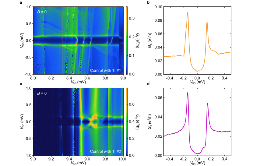
Supplementary Fig. 2 shows the tunneling spectrum of two evaporated control devices with Ti sticking layers. Both devices are switchy (discontinuities in ), but compared to devices without a Ti sticking layer, it is now possible to move away from the SGRs and extract a minimum normalized sub-gap conductance. It is also possible to identify odd and even Coulomb valleys by the SGRs and the Kondo resonances. Supplementary Figs. 2b and 2d show conductance traces at values indicated by the orange and purple lines in Supplementary Figs. 2a and 2c.
I.3 Epitaxial full-shell QPC device
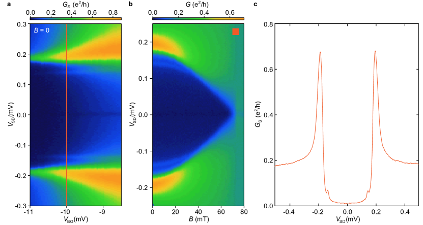
Additional data on the single ABS in the epitaxial full-shell QPC device is shown in Supplementary Fig. 3. Data shown in Supplementary Fig. 3a is identical to data shown in Fig. 2a in the main text. Here, we change the aspect ratio to place emphasis on the ABS. Supplementary Fig. 3b shows the evolution of the induced gap and the ABS as a function of magnetic field. The ABS remains close to the gap edge, then merges into the continuum above 40 mT. It shows up most prominently as two peaks in an one-dimensional trace taken at -10 V (Supplementary Fig. 3c).
I.4 Epitaxial full-shell QD device
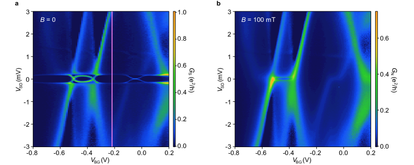
We turn our attention to measurements from epitaxial full-shell QD devices. Distinct Coulomb diamond resonances with charging energy on the order of 1 meV can be seen in Supplementary Fig. 4. Furthermore, even-odd structure can be seen from the presence of both Kondo resonances (normal state) and SGRs (superconducting state) in alternating Coulomb diamonds. QD data shown in Fig. 3d (main text) is taken at the particle-hole symmetry point of an even Coulomb diamond (pink line in Supplementary Fig. 4a).
I.5 Epitaxial half-shell QD device
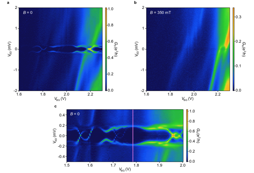
Three epitaxial half-shell QD devices were measured. In Supplementary Figs. 5a and 5b we show the charge stability diagrams of one of the devices at zero and finite magnetic fields. The QD nature of this device is evident from Coulomb diamonds, and its charging energy is on the order of 1 meV. In the normal state (Supplementary Fig. 5b), we see a pair of spin-split Kondo resonances near 2.2 V. In the superconducting state, the Kondo resonance turns into a pair of SGRs (Supplementary Fig. 5a). To extract a measurement of the induced gap, we move away from the SGRs in . Data shown in Fig. 5c (main text) is taken at a backgate voltage value indicated by the pink line in Supplementary Fig. 5c.