Plasmonics in Atomically Thin Materials
Abstract
The observation and electrical manipulation of infrared surface plasmons in graphene have triggered a search for similar photonic capabilities in other atomically thin materials that enable electrical modulation of light at visible and near-infrared frequencies, as well as strong interaction with optical quantum emitters. Here, we present a simple analytical description of the optical response of such kinds of structures, which we exploit to investigate their application to light modulation and quantum optics. Specifically, we show that plasmons in one-atom-thick noble-metal layers can be used both to produce complete tunable optical absorption and to reach the strong-coupling regime in the interaction with neighboring quantum emitters. Our methods are applicable to any plasmon-supporting thin materials, and in particular, we provide parameters that allow us to readily calculate the response of silver, gold, and graphene islands. Besides their interest for nanoscale electro-optics, the present study emphasizes the great potential of these structures for the design of quantum nanophotonics devices.
I Introduction
Plasmons –the collective electron oscillations in nanostructured conductors– allow us to control light at the nanometer scale, particularly using the large concentration and enhancement of electromagnetic intensity that they generate Li et al. (2003). Additionally, and unlike other optical excitations in small systems (e.g., atomic and molecular quantum emitters), plasmons display a powerful combination of two appealing properties: they are robust (i.e., they are not destroyed by the presence of a dielectric environment) and they interact strongly with light (e.g., they display excitation cross-sections typically exceeding the projected area of the nanostructures that sustain the plasmons). These features have facilitated the use of plasmons in applications as varied as nonlinear optics Danckwerts and Novotny (2007); Davoyan et al. (2008); Palomba and Novotny (2008); Metzger et al. (2014), ultrasensitive detection down to the single-molecule level via surface-enhanced Raman scattering (SERS) Kneipp et al. (1997); Nie and Emory (1997); Xu et al. (1999); Rodríguez-Lorenzo et al. (2009), cancer diagnosis and therapy O’Neal et al. (2004); Loo et al. (2005); Gobin et al. (2007); Jain et al. (2007, 2008); Qian et al. (2008), quantum information processing Chang et al. (2006); Dzsotjan et al. (2010); Savasta et al. (2010); Manjavacas et al. (2011), improved photovoltaics Atwater and Polman (2010); White and Catchpole (2012), and subwavelength lithography Dong et al. (2014). Optical metamaterials are also largely relying on subwavelength plasmons to display properties that are not available in naturally occurring materials Engheta (2007); Zheludev (2010); Boardman et al. (2010). These efforts are due in part to the impressive progress made in nanofabrication Nagpal et al. (2009) and colloid chemistry Grzelczak et al. (2008); Fan et al. (2010) techniques, as well as in the theoretical understanding of the response of nanometallic structures Halas et al. (2011); Solís et al. (2014).
The field of plasmonics has been quite focused on noble metals, which are generally regarded as prototypical plasmonic materials, although they suffer from relatively large inelastic losses that limit the lifetime of plasmons down to a few optical cycles in deep-subwavelength structures. In this context, a search for better plasmonic materials has been initiated with a view to reducing absorption West et al. (2010); Feigenbaum et al. (2010); Boltasseva and Atwater (2011); Naik et al. (2013). Recently, highly doped graphene has emerged as a promising alternative Vakil and Engheta (2011); Koppens et al. (2011); Nikitin et al. (2011); Ju et al. (2011); Fei et al. (2011); Bludov et al. (2012); Chen et al. (2012); Fei et al. (2012); Fang et al. (2013); Brar et al. (2013); García de Abajo (2014), combining huge field confinement and enhancement with comparatively lower losses Fang et al. (2013); Woessner et al. (2015), as well as large electrical tunability of its optical response Wang et al. (2008); Mak et al. (2008); Li et al. (2008a); Chen et al. (2011). These properties hold great potential for electro-optics applications, such as fast light modulation via electrostatic gating Ju et al. (2011); Fei et al. (2011); Chen et al. (2012); Fei et al. (2012); Fang et al. (2013); Brar et al. (2013), which has been demonstrated with the achievement of frequency variations spanning a whole octave Fang et al. (2013).
Unfortunately, plasmons in graphene, as well as in other so-called two-dimensional crystals Scholz et al. (2013) and in topological insulators Di Pietro et al. (2013), have so far been observed at mid-infrared (mid-IR) and lower frequencies, as they are limited by the low carrier densities in these materials. In contrast, atomically thin metals already possess a substantial conduction electron density in their undoped state, thus sustaining plasmons in the visible and near-infrared (vis-NIR), which are spectral ranges with better prospects for technological applications. Additionally, atomically thin noble metal nanoislands can undergo strong interaction with light and exhibit significant electrical tunability Manjavacas and García de Abajo (2014), as the doping levels that are currently attainable using gating technology can produce substantial fractional changes in the conduction electron density.
Plasmons in metal clusters of atomic dimensions have been examined and optically characterized for a long time Ekardt and Pacheco (1992), and they have even been used as a toolbox to test the ability of different first-principles computational methods to simulate optical and electron-based spectroscopic measurements Onida et al. (2002). In a separate effort, atomic self-assembly has been used to produce monoatomic gold wires Losio et al. (2001), which were later shown to sustain extremely confined plasmons Nagao et al. (2006). Similar low-dimensional plasmons have been experimentally characterized using electron spectroscopy in ultrathin indium Chung et al. (2010) and silicide Rugeramigabo et al. (2010) wires, as well as in few-atomic-layer silver films Moresco et al. (1999) and monolayer DySi2 Rugeramigabo et al. (2008). Unfortunately, no further exploration has been pursued towards the coupling of propagating light to these systems and their application to nanophotonics.
Motivated by the availability of these atomically thin materials and their potential for nanophotonics applications, we present here a simple analytical study of the optical properties of disks and ribbons, accompanied by a discussion of their ability to achieve tunable complete optical absorption and quantum strong coupling between plasmons and optical emitters.
II Optical response and tunability of 2D metallic nanoislands
We describe thin metals in terms of a frequency-dependent 2D conductivity , which is related to the bulk dielectric function of the material through , where is the film thickness. This local approximation works well for atomically thin islands of noble metals with a lateral extension above nm, as shown by comparison with quantum-mechanical simulations based upon the random-phase approximation Manjavacas and García de Abajo (2014). In the low-frequency limit, the dielectric function is well approximated by the Drude model , where is the bulk classical plasmon frequency and is a phenomenological relaxation rate. Combining these two expressions for , we find the 2D conductivity to reduce to
| (1) |
This formula can even be applied to include the full dependence of the measured dielectric function by simply allowing and to depend on . In noble metals, these parameters are relatively independent of frequency over the NIR spectral range (see Fig. 5 in Appendix D). The present formalism can also describe graphene, where depends on the Fermi energy relative to the so-called Dirac point as (for example, for a nominal graphene thickness nm, as extracted from the interlayer distance in graphite, and considering a realistic value of the Fermi energy eV Chen et al. (2011), we have eV).
The far-field response of islands that are small compared with the light wavelength can be expressed in terms of their polarizability , which admits simple approximate expressions under the reasonable assumption that the lowest-order dipole mode dominates the spectral strength. More precisely, using the expressions derived in Appendix A, we find
| (2) |
where is the area of the island and is its lowest-order plasmon frequency (see Table 1 for disks and ribbons). In particular, for a disk of diameter and thickness placed at the planar interface between two media of permittivities and , we have (see Table 1 and derivation in Appendix A)
| (3) |
where .
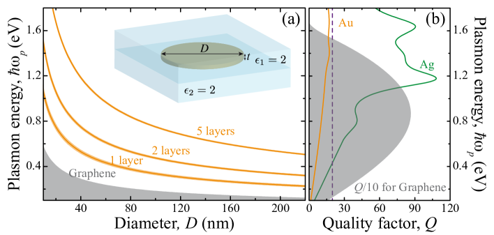
Figure 1(a) shows the values of predicted by Eq. (3) for gold, silver, and graphene disks embedded in silica. We consider noble metal disks consisting of 1, 2, or 5 atomic monolayers, which can clearly reach the NIR. In contrast, the shaded area shows that the plasmon energies lie in he mid-IR, even for relatively high doping levels (eV).
We note that the quality factor of the plasmon resonances (i.e., times the number of optical cycles for which the intensity has decayed by ) is given by and is in fact independent of shape in the electrostatic limit under consideration (). Here, is the Drude damping of Eq. (1), which depends on frequency and material as shown in Fig. 5 (Appendix D), leading to the dependence of on illustrated by Fig. 1(b). High-quality (mobility cm) highly doped (eV) graphene exceeds the performance of gold but is below that of silver for plasmon energies above eV, which are only reachable with graphene structures that are smaller than those considered in Fig. 1 García de Abajo (2014), although edge effects can then introduce important corrections Thongrattanasiri et al. (2012a); Manjavacas et al. (2013a).
The range of electro-optical tunability of graphene disk plasmons is illustrated by the shaded area in Fig. 1(a). For a given disk diameter, the plasmon energy can be moved up to the upper value of that area when the doping is increased up to eV. For silver and gold, the range of tunability is lower than in graphene, although it has the advantage that the plasmons are in the NIR. Nonetheless, using currently available gating technology, under the same doping conditions that allow achieving a graphene Fermi energy , corresponding to a charge carrier density cm-2, we obtain a fractional variation of the plasmon energy in gold and silver, where cm-2 is the areal density of conduction electrons in these metals. This produces an overall fractional variation of the plasmon that is resolvable with a quality factor , represented by the dashed vertical line of Fig. 1(b), which is clearly within reach with silver.
III Coupling to Quantum Emitters
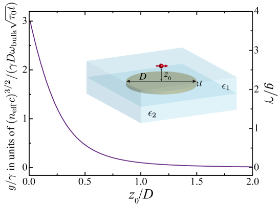
The large concentration of electromagnetic energy associated with the plasmons of atomically thin structures can lead to strong interaction with nearby quantum emitters. This idea has been recently explored in graphene Koppens et al. (2011); Manjavacas et al. (2012); Huidobro et al. (2012) and we elaborate on it here to produce a semi-analytical model that is directly applicable to any thin conducting material. For this purpose, we introduce the 2D charge density associated with the plasmon as a function of position along the metal island. This quantity can be conveniently normalized for one plasmon, as discussed in Appendix B, where analytical expressions are given for the lowest-order dipole modes of disks and ribbons (see Table 1). Intuitively, plays a similar role as the charge density associated with the transition of one electron between the bound states and of a confined system. We now consider a two-level quantum emitter (e.g., an atom or molecule) of transition dipole . Taking the metal island to lie in the plane and the emitter at position , the electrostatic emitter-plasmon interaction is simply given by
| (4) |
where the integral is extended over the area of the island, is defined right after Eq. (3), and is the effective emitter transition dipole, which is related to its radiative lifetime in the absence of the island through . Incidentally, is the transition dipole in vacuum multiplied by a local-field correction Yablonovitch et al. (1988).
The quantum evolution of the emitter-plasmon system can be described by the Hamiltonian Koppens et al. (2011); Manjavacas et al. (2012)
| (5) |
where and ( and ) are the annihilation (creation) operators of the plasmon and the emitter excitation of energies and , respectively. Let us stress that we are using the same rate of emitter-plasmon coupling as defined by the electrostatic energy of Eq. (4). In the Hamiltonian (5) we are neglecting the direct interaction of the time-dependent external field with the emitter, as its dipole is assumed to be small compared with the plasmon dipole
Incidentally, the normalization of for a single plasmon is actually based on this dipole, as explained in Appendix B.
The lifetime of the emitter and the plasmon decay rate can be introduced in the quantum description of the combined system through the density matrix , which follows the equation of motion Ficek and Tanas (2002); Meystre and Sargent (2007)
| (6) |
In this formalism, we can calculate the polarizability by first obtaining the expected value of the induced dipole from upon illumination with a weak external field We find the induced dipole to admit the form , thus defining . In the absence of the emitter (i.e., taking ), we recover a polarizability as given by the term of Eq. (18), thus demonstrating the self-consistency of our plasmon-normalization scheme. Additionally, when the combined system is considered, the linear polarizability becomes with
For , this expression exhibits two poles at frequencies , yielding a vacuum Rabi splitting given by .
For the vacuum Rabi splitting to be observable, it must be larger than the width of the plasmon peak, that is, . This condition signals the so-called strong-coupling regime, which has been argued to be achievable in graphene Koppens et al. (2011). In this regime, the bosonic plasmon state mixes with the fermionic two-level emitter to produce a Jaynes-Cummings ladder of hybridized states Jaynes and Cummings (1963), which has been predicted to produce non-classical statistics of the plasmon population upon external illumination, as well as nonlinear optical response Manjavacas et al. (2012) (i.e., the nonlinearity of the quantum emitter is inherited by the combined plasmon-emitter system).
It should be noted that the decay rate of the excited emitter is enhanced by the coupling to the plasmon and becomes for
| (7) |
under the condition that the fraction in this expression is small (weak coupling). This well-known result is rederived in Appendix C from Eqs. (5) and (6), and we also show that the dielectric formalism of Appendix A reproduces Eq. (7) with as defined by Eq. (4), provided the plasmon charge density is normalized as prescribed in Appendix B, thus demonstrating the self-consistency of the theoretical methods elaborated in this work.
Equipped with the analytical model for the plasmons of thin conductor islands discussed in the Appendix, we examine in Fig. 2 the ratio , where is calculated from Eq. (4) using the analytical expression of for a disk plasmon given in Table 1. We find to depend on the lifetime of the emitter , the Drude parameters of the conducting disk and (see Eq. (1)), the disk diameter and thickness and , and the index of refraction of the surrounding medium only through a multiplicative coefficient . We plot in Fig. 2 expressed in units of that coefficient (left scale) as a function of the distance between the emitter and the center of the disk. The emitter dipole is assumed to be parallel to the graphene. The right scale shows the ratio calculated for eV and eV, typical of gold in the NIR, with ns, nm, nm (i.e., one (111) atomic layer), and . This result indicates that the strong-coupling regime is reachable over a wide range of distances using gold islands. Silver structures should produce larger coupling because is smaller in that material (see Fig. 5). Further confinement of the plasmons in structures that display hotspots, such as bowtie antennas Thongrattanasiri and García de Abajo (2013), could lead to even larger values of .
Decoherence produced by inelastic transitions can severely damage the efficiency of quantum emitters when they are placed in a solid-state environment, although close to 100% efficiencies can be achieved with organic molecules under cryogenic conditions Rezus et al. (2012). Fortunately, the enhancement of the coupling rate from the emitter to the plasmon at the frequency of the latter can decrease the relative importance of inelastic decay channels in the emitter (e.g., coupling to phonons of the surrounding material, Auger processes, etc.), so that in practice the coherent part of the decay in emitters such as nitrogen-vacancies in diamond, in which the zero-phonon elastic channel accounts for only a small fraction of the emission, can be enhanced by coupling to the nanoisland, and we are thus under similar conditions as those considered in this study (i.e., the emitter decay through coupling to a plasmon dominates over other inelastic channels).
IV Complete Optical Absorption
Complete optical absorption has been studied and observed over many frequency ranges in disordered metal films Hunderi and Myers (1973); Kravets et al. (2010), through lattice resonances in gratings and planar metamaterials Hutley and Maystre (1976); Maystre and Petit (1976); Popov and Tsonev (1990); Tan et al. (2000); Greffet et al. (2002); Landy et al. (2008); García de Abajo (2007), assisted by localized plasmonic resonances Kachan et al. (2006); Teperik et al. (2008), using multilayer structures Collin et al. (2004), and in overdense plasma Bliokh et al. (2005). However, the possibility of achieving complete optical absorption in atomically thin films offers additional advantages, as we discuss below.
It is well known that the maximum absorbance produced by an optically thin film in a homogeneous environment is 50%: the incident light induces charges and currents that have no memory of where light is coming from, and therefore, they radiate symmetrically towards both sides of the film with a scattered wave amplitude ; consequently, the reflected and transmitted amplitudes are and , where the first term in the transmission is the incident field of unit amplitude; the absorbance is thus , whose maximum value is as a function of the complex variable . Now, with the addition of a reflecting screen on one side of the film, light can make two passes through the thin material, producing a maximum of 100% absorption if both incident and reflected waves are in phase at that plane. This is the so-called Salisbury screen configuration, in which the film/metal-screen separation should be roughly Fante and McCormack (1988); Engheta (2002) (i.e., a phase of is produced by the metallic reflection and another contribution comes from phase associated with the round trip propagation between the film and the screen, assumed to be embedded in an environment of refractive index ).
These ideas have been recently explored for graphene, leading to the prediction of complete optical absorption by a suitably patterned carbon layer Thongrattanasiri et al. (2012b); Ferreira and Peres (2012), under the condition that the extinction cross-section per unit cell element is of the order of the unit cell area. The observation of electrically tunable large absorbance in patterned graphene has been recently accomplished Fang et al. (2014); Jang et al. (2014). We argue here that similar levels of tunable absorption are achievable using noble metals.
It is instructive to first examine the maximum extinction of a thin island in vacuum. The corresponding cross section is van de Hulst (1981) , which upon insertion of Eq. (2) is found to exhibit a maximum at , given approximately by . Remarkably, this maximum extinction is independent of shape for a given area of the island, under the assumption that an individual plasmon mode dominates the extinction. In particular, for single atomic layers of gold (silver) films (nm), considering the plasmon energy to be in the NIR, we have eV and meV (meV), so that the maximum cross section is () times the area of the island. For highly doped graphene, this number is even larger due to the comparatively lower losses of this material (see Fig. 5).
Complete optical absorption is achievable in periodic arrays placed above a Salisbury screen. The normal-incidence reflection coefficient of a doubly-periodic array of small period compared with the light wavelength, surrounded by a homogeneous environment of refractive index , reduces to Thongrattanasiri et al. (2012b)
where , , is the unit cell area, and is a number that depends on symmetry (e.g., and for hexagonal and square arrays, respectively, assuming that all islands interact through their induced dipoles; corrections due to nearest-neighbor interactions beyond dipolar terms are possible for closely spaced islands, in which case the coefficient can depend on their shape). With a Salisbury screen of reflectivity separated a distance from the array, the incident and reflected waves are exactly on phase when is a multiple of . Complete absorption is then produced under the condition , which is satisfied at a frequency given by , where , provided we have
| (8) |
Interestingly, this condition for complete optical absorption is also independent of the shape of the island. Using the approximate values of and noted above for gold and silver in the NIR, and considering for simplicity a non-absorbing Salisbury screen () and a glass environment (), the condition (8) for perfect absorption in gold (silver) arrays is fulfilled with a fraction (0.29) between the areas of the island and the unit cell. Consequently, this condition can be easily met using silver atomic monolayers, and also with multilayers of either gold or silver.
Incidentally, similar results are obtained for ribbon arrays of period García de Abajo (2014). Then, the condition (8) remains unchanged, with , where is the ribbon width. Because of the ribbon translational symmetry, we work with 2D rather than 3D scattering, so we need to redefine , and . The frequency at which complete absorption occurs is then , where (see Table 1).
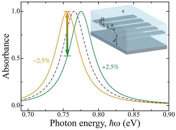
It is important to note that the value of can be modulated by using currently available gating technology (see above), and this in particular produces peak shifts larger than the peak width in silver (see Fig. 1(b)), as shown in Fig. 3 for an illustrative example. This type of structure is convenient because the ribbons can be contacted at a large distance away from the region in which the optical modulation is pursued. Besides, the strong absorption only occurs for polarization across the ribbons, thus suggesting a possible application as tunable polarizers.
V Outlook and Perspectives
Graphene plasmons are focusing much attention due in part to the demonstrated ability to modulate their frequencies by electrically doping the carbon layer through suitably engineered gates Ju et al. (2011); Fei et al. (2011); Chen et al. (2012); Fei et al. (2012); Fang et al. (2013); Brar et al. (2013). This modulation can be potentially realized at high speeds, as the number of charge carriers that are needed to produce changes in the Fermi energy of the order of the electronvolt is relatively small, and consequently, so they are the inductance and capacitance associated with the graphene itself. Unfortunately, graphene plasmons have only been observed at mid-infrared and lower frequencies. Moving to the vis-NIR is challenging and requires patterning structures with sizes nm under realistically attainable doping conditions. In this respect, molecular self-assembly provides a viable way of synthesizing nanographenes in this size range Li et al. (2008b, 2013); Cai et al. (2010); Müllen (2014). Doped carbon nanotubes have also been predicted to display plasmons that are rather insensitive to their degree of chirality García de Abajo (2014), and therefore, they provide a viable route towards the fabrication of large-scale tunable plasmonic structures operating in the vis-NIR regime. Polycyclic aromatic hydrocarbons also sustain excitations at vis-NIR frequencies that behave as graphene plasmons Manjavacas et al. (2013b) and constitute promising candidates to advance towards atomic-scale tunable plasmonics.
Although plasmons in atomically thin metals have been observed in several systems Nagao et al. (2006); Chung et al. (2010); Rugeramigabo et al. (2010); Moresco et al. (1999); Rugeramigabo et al. (2008), these studies have focused on extended surfaces whose plasmon dispersion relations are far from the light cone, thus averting the possibility of direct coupling to propagating light. Further patterning of these types of surfaces into disks and ribbons such as those considered here could facilitate the coupling to optical probes. An alternative option consists in decorating atomically thin films with dielectric colloids to provide periodic optical contrast. Substrate pre-patterning of disks, ribbons, or other morphologies, followed by atomic layer deposition constitutes yet another possibility.
We conclude that atomically thin materials hold great potential for the manipulation of light at truly nanometer scales and for the development of applications to optical signal processing, quantum optics, and sensing. We should emphasize that small nanoparticles, not necessarily atomically thin, can produce similar levels of strong-coupling and optical absorption as discussed above for thin films, although they are not tunable using electrical gates because the injected charge carriers have to compete with a much larger number of bulk conduction electrons. The great opportunities offered by these materials are however accompanied by formidable challenges to produce the islands at designated positions and with controlled morphology, possibly requiring a combination of top-down patterning and bottom-up self-assembly methods similar to those mentioned above.
Appendix A OPTICAL RESPONSE OF THIN METAL ISLANDS IN THE ELECTROSTATIC LIMIT
The scale-invariant character of the electrostatic problem (i.e., the absence of a frequency-dependent length scale imposed by the wavelength) has been used on several ocations to express the solutions in terms of modal expansions Bergman (1979); Ghosh and Fuchs (1988); Ouyang and Isaacson (1989); Bergman and Dunn (1992). Here, we formulate a suitable decomposition for optically thin structures. We consider islands of small characteristic size (e.g., the diameter for disks or the width for ribbons) compared with the light wavelength, such that the optical electric field can be expressed in terms of a scalar potential . The islands are however taken to be large enough to be described as infinitesimally thin domains characterized by a local, frequency-dependent 2D conductivity . Following previous analyses for graphene Fang et al. (2013); García de Abajo (2013, 2014), we write the self-consistent potential at positions in the plane of the island as
| (9) |
which is the sum of the external perturbation and the contribution produced by the induced charges (integral term). The island is chosen to lie at the planar interface between two media of permittivities and , which contribute to the above expression through a factor multiplying the in-plane Coulomb potential, where
| (10) |
Now, using the definitions and
taking the gradient in both sides of Eq. (9), and multiplying by , we find García de Abajo (2013)
| (11) |
where
whereas is a filling function that is 1 if lies on the metal and zero otherwise, so that the frequency and spatial dependences of the conductivity are separated as . Notice that this formalism is also valid for inhomogeneous layers by allowing to take values different from 0 or 1 Thongrattanasiri et al. (2012c). Here, we have defined , which is a real, symmetric operator that admits a complete orthonormal set of real eigenvectors and eigenvalues satisfying the relations
Then, the solution to Eq. (11) reduces to
| (12) |
where .
Applying these results to a uniform external field aligned with a symmetry direction of the island (i.e., for ), we obtain the polarizability along that direction from the induced density
| (13) |
Inserting Eq. (12) into this expression, we obtain
| (14) |
where runs over eigenmodes of the system and
| (15) |
are dimensionless coupling coefficients. Using the conductivity of Eq. (1), we can recast Eq. (14) as
| (16) |
where the plasmons of the nanoisland can be identified with modes of negative eigenvalues and frequencies
| (17) |
corresponding to the poles of Eq. (16).
| disk | ||||
|---|---|---|---|---|
| ribbon |
Equation (16) involves coefficients that are subjected to two useful sum rules García de Abajo (2014):
-
i.
For any arbitrarily shaped island of area , we have . This result is readily obtained from the definition of the coefficients in Eq. (15) upon application of the closure relation for (see above). Applying this sum to a Drude metal (i.e., for frequency-independent ), we conclude that the integral of the extinction cross-section () is actually proportional to , which is in turn proportional to the number of electrons (i.e., it fulfills the -sum rule Pines and Nozières (1966)).
-
ii.
Another sum rule follows from Eq. (14) in the limit (i.e., when the island behaves as a perfect conductor, so that ). Without loss of generality, we can consider a freestanding island (), so we have . Now, for in-plane polarization of a disk of diameter , we have (this result can be derived from the polarizability of an ellipsoid of vanishing height García de Abajo (2007)), which leads to . Likewise, from the transversal polarizability of a thin metal ribbbon of width van de Hulst (1981) (, where is the length), we find .
Interestingly, for these types of structures and polarizations, we find one single mode to be dominant and to absorb most of the weight in the above sums García de Abajo (2014). More precisely, this is the lowest-order dipole plasmon. Neglecting all other modes, these sum rules lead to the values of , , and listed in Table 1 and extensively used throughout this work to produce analytical estimates of plasmonic behavior.
Appendix B CHARGE INDUCED BY A SINGLE PLASMON
We introduce a purely electrostatic scheme to normalize the induced charge density associated with a single plasmon . From linear-response theory Pines and Nozières (1966), the polarizability reads
| (18) |
where
| (19) |
is the dipole moment associated with mode for polarization along a symmetry direction . Now, in order to compare Eq. (18) with Eq. (16), we neglect in front of and approximate Eq. (18) as
| (20) |
Now, inserting the Drude conductivity of Eq. (1) into Eq. (14), comparing the result with Eq. (20), and taking Eq. (17) into account, we find the normalization condition
| (21) |
Within the single-mode approximation noted at the end of the previous paragraph, writing the charge density associated with the lowest-order disk dipole plasmon as , where gives the radial dependence, we find the normalization condition
Similarly, the plasmon charge density along the transversal direction of a ribbon contained in the region satisfies
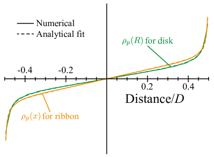
where is the ribbon area (with ) and we have utilized the symmetry . Using these normalizations, we find that the analytical expressions for that are given in Table 1, where the density profile is taken to fit previous calculations Silveiro and García de Abajo (2014); Thongrattanasiri et al. (2012c) based upon the boundary-element method. Actually, these formulas reproduce rather well the calculated density profiles, as shown in Fig. 4.
An alternative normalization is provided by the fact that the plasmon energy is twice its electrostatic energy. This condition can be expressed as
which leads to values of the normalization coefficients and for disks and ribbons, respectively, in excellent agreement with those shown in the caption of Table 1, considering that we are making the approximation that only the lowest-order plasmon contributes to the response. Additionally, we show in Appendix C that the plasmon normalization here introduced is the same as that needed to describe the coupling rate between the plasmon and an optical emitter through the intuitive expression given in Eq. (4).
Appendix C PLASMON-ENHANCED EMITTER DECAY RATE
C.1 Density-matrix approach
It is convenient to expand the density matrix of Eq. (6) as
| (22) |
where are time-dependent coefficients, while denotes a state with plasmons accompanied by the excited (de-excited) emitter for (). Inserting this expression into Eq. (6), we find
| (23) |
where . We now argue that, for an initial density matrix in which all terms of Eq. (22) with or are zero (i.e., a density matrix involving a maximum number of excitations in the combined plasmon-emitter system), the last term of Eq. (23) vanishes because it involves states that are never populated. We are then left with a self-contained subset of equations involving coefficients with . For this manifold of excitations, we trivially find solutions , where the coefficients satisfy the equations
and admit the familiar Jaynes-Cummings solutions Jaynes and Cummings (1963)
with . In the limit, we have and , so the solution with the upper (lower) signs has () at , and therefore it corresponds to the initially excited (de-excited) emitter. The decay rate of the emitter when it is initially excited and the plasmon is not populated (i.e., starting from ) is then given by the decay of the term of Eq. (22) in the upper-sign solution. We find , which reduces to Eq. (7) under the condition .
C.2 Dielectric approach
The decay rate of an emitter placed at a position in the vicinity of the plasmonic structure can be related to its transition dipole as Novotny and Hecht (2006)
| (24) |
where is the self-induced electric field produced by a dipole located at . We can calculate this field from the dielectric formalism of Appendix A using the induced density of Eq. (13), but now the coefficients of Eq. (12) have to be obtained from the external dipole field , where is defined in Eq. (10). (Notice that the potential produced by the dipole at the planar interface between media of permittivities and is the same as in vacuum multiplied by .) After some algebra, we find
| (25) |
Inserting Eq. (25) into Eq. (24), and retaining only the term, we recover the emitter decay rate given by Eq. (7) with the exact same definition of the coupling rate as given by Eq. (4), provided we define
Finally, inserting this expression into Eq. (19), integrating by parts, and keeping in mind the definition of in Eq. (15), we recover Eq. (21) for the plasmon transition strength. Therefore, we conclude that the normalization of the plasmon charge density discussed in Appendix B, based upon the polarizability of the plasmonic structure, produces the same decay rate of a neighboring emitter when calculated either following the semi-classical dielectric formalism described in this paragraph or using the density-matrix formalism with the intuitive coupling rate defined by Eq. (4).
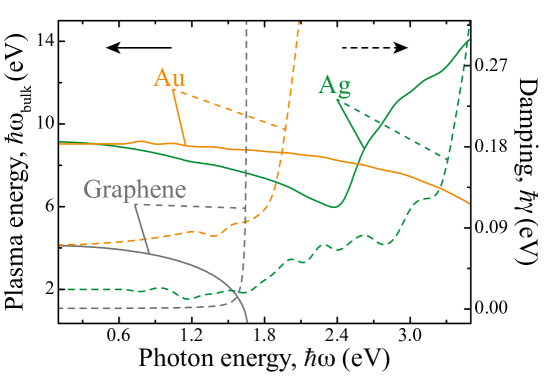
Appendix D DRUDE PARAMETERS FOR NOBLE METALS AND GRAPHENE
We show in Fig. 5 the Drude parameters and for silver, gold, and graphene. For noble metals, we obtain these parameters by fitting the measured dielectric function of the material Johnson and Christy (1972) to the expression . For graphene, we use the local-RPA conductivity Falkovsky and Varlamov (2007); Koppens et al. (2011), which we correct in the following expression to simultaneously account for inelastic attenuation and finite temperature in both intraband and interband transitions García de Abajo (2014):
| (26) |
where is the Fermi-Dirac distribution as a function of electron energy and Fermi energy . The first term inside the integral of Eq. (26), which corresponds to intraband electron-hole pair transitions within the partially occupied Dirac cones of the doped carbon layer, can be integrated analytically to yield a contribution with . The second term, which originates in interband transitions between lower and upper Dirac cones, needs to be integrated numerically. In Fig. 5, we represent and for graphene by fitting Eq. (1) to the values of calculated from Eq. (26).
Acknowledgements.
This work has been supported in part by the European Commission (Graphene Flagship CNECT-ICT-604391 and FP7-ICT-2013-613024-GRASP). A. M. acknowledges financial support from the Welch foundation through the J. Evans Attwell-Welch Postdoctoral Fellowship Program of the Smalley Institute of Rice University (Grant No. L-C-004).References
- Li et al. (2003) K. R. Li, M. I. Stockman, and D. J. Bergman, Phys. Rev. Lett. 91, 227402 (2003).
- Danckwerts and Novotny (2007) M. Danckwerts and L. Novotny, Phys. Rev. Lett. 98, 026104 (2007).
- Davoyan et al. (2008) A. R. Davoyan, I. V. Shadrivov, and Y. S. Kivshar, Opt. Express 16, 21209 (2008).
- Palomba and Novotny (2008) S. Palomba and L. Novotny, Phys. Rev. Lett. 101, 056802 (2008).
- Metzger et al. (2014) B. Metzger, M. Hentschel, T. Schumacher, M. Lippitz, X. Ye, C. B. Murray, B. Knabe, K. Buse, and H. Giessen, Nano Lett. 14, 2867 (2014).
- Kneipp et al. (1997) K. Kneipp, Y. Wang, H. Kneipp, L. T. Perelman, I. Itzkan, R. R. Dasari, and M. S. Feld, Phys. Rev. Lett. 78, 1667 (1997).
- Nie and Emory (1997) S. Nie and S. R. Emory, Science 275, 1102 (1997).
- Xu et al. (1999) H. Xu, E. J. Bjerneld, M. Käll, and L. Börjesson, Phys. Rev. Lett. 83, 4357 (1999).
- Rodríguez-Lorenzo et al. (2009) L. Rodríguez-Lorenzo, R. A. Álvarez-Puebla, I. Pastoriza-Santos, S. Mazzucco, O. Stéphan, M. Kociak, L. M. Liz-Marzán, and F. J. García de Abajo, J. Am. Chem. Soc. 131, 4616 (2009).
- O’Neal et al. (2004) D. P. O’Neal, L. R. Hirsch, N. J. Halas, J. D. Payne, and J. L. West, Cancer Lett. 209, 171 (2004).
- Loo et al. (2005) C. Loo, A. Lowery, N. J. Halas, J. L. West, and R. Drezek, Nano Lett. 5, 709 (2005).
- Gobin et al. (2007) A. M. Gobin, M. H. Lee, N. J. Halas, W. D. James, R. A. Drezek, and J. L. West, Nano Lett. 7, 1929 (2007).
- Jain et al. (2007) P. K. Jain, I. H. El-Sayed, and M. A. El-Sayed, Nanotoday 2, 18 (2007).
- Jain et al. (2008) P. K. Jain, X. H. Huang, I. H. El-Sayed, and M. A. El-Sayed, Accounts Chem. Res. 41, 578 (2008).
- Qian et al. (2008) X. Qian, X.-H. Peng, D. O. Ansari, Q. Yin-Goen, G. Z. Chen, D. M. Shin, L. Yang, A. N. Young, M. D. Wang, and S. Nie, Nat. Biotech. 26, 83 (2008).
- Chang et al. (2006) D. E. Chang, A. S. Sörensen, P. R. Hemmer, and M. D. Lukin, Phys. Rev. Lett. 97, 053002 (2006).
- Dzsotjan et al. (2010) D. Dzsotjan, A. S. Sörensen, and M. Fleischhauer, Phys. Rev. B 82, 075427 (2010).
- Savasta et al. (2010) S. Savasta, R. Saija, A. Ridolfo, O. Di Stefano, P. Denti, and F. Borghese, ACS Nano 4, 6369 (2010).
- Manjavacas et al. (2011) A. Manjavacas, F. J. García de Abajo, and P. N. Nordlander, Nano Lett. 11, 2318 (2011).
- Atwater and Polman (2010) H. A. Atwater and A. Polman, Nat. Mater. 9, 205 (2010).
- White and Catchpole (2012) T. P. White and K. R. Catchpole, Appl. Phys. Lett. 101, 073905 (2012).
- Dong et al. (2014) J. Dong, J. Liu, G. Kang, J. Xie, and Y. Wang, Sci. Rep. 4, 5618 (2014).
- Engheta (2007) N. Engheta, Science 317, 1698 (2007).
- Zheludev (2010) N. I. Zheludev, Science 328, 582 (2010).
- Boardman et al. (2010) A. D. Boardman, V. V. Grimalsky, Y. S. Kivshar, S. V. Koshevaya, M. Lapine, N. M. Litchinitser, V. N. Malnev, M. Noginov, Y. G. Rapoport, and V. M. Shalaev, Laser Photon. Rev. 5, 287 (2010).
- Nagpal et al. (2009) P. Nagpal, N. C. Lindquist, S. H. Oh, and D. J. Norris, Science 325, 594 (2009).
- Grzelczak et al. (2008) M. Grzelczak, J. Pérez-Juste, P. Mulvaney, , and L. M. Liz-Marzán, Chem. Soc. Rev. 37, 1783 (2008).
- Fan et al. (2010) J. A. Fan, C. H. Wu, K. Bao, J. M. Bao, R. Bardhan, N. J. Halas, V. N. Manoharan, P. Nordlander, G. Shvets, and F. Capasso, Science 328, 1135 (2010).
- Halas et al. (2011) N. J. Halas, S. Lal, W. Chang, S. Link, and P. Nordlander, Chem. Rev. 111, 3913 (2011).
- Solís et al. (2014) D. M. Solís, J. M. Taboada, F. Obelleiro, L. M. Liz-Marzán, and F. J. García de Abajo, ACS Nano 8, 7559 (2014).
- West et al. (2010) P. R. West, S. Ishii, G. V. Naik, N. K. Emani, V. M. Shalaev, and A. Boltasseva, Laser Photonics Rev. 4, 795 (2010).
- Feigenbaum et al. (2010) E. Feigenbaum, K. Diest, and H. A. Atwater, Nano Lett. 10, 2111 (2010).
- Boltasseva and Atwater (2011) A. Boltasseva and H. A. Atwater, Science 331, 290 (2011).
- Naik et al. (2013) G. V. Naik, V. M. Shalaev, and A. Boltasseva1, Adv. Mater. 25, 3264 (2013).
- Vakil and Engheta (2011) A. Vakil and N. Engheta, Science 332, 1291 (2011).
- Koppens et al. (2011) F. H. L. Koppens, D. E. Chang, and F. J. García de Abajo, Nano Lett. 11, 3370 (2011).
- Nikitin et al. (2011) A. Y. Nikitin, F. Guinea, F. J. García-Vidal, and L. Martín-Moreno, Phys. Rev. B 84, 161407(R) (2011).
- Ju et al. (2011) L. Ju, B. Geng, J. Horng, C. Girit, M. Martin, Z. Hao, H. A. Bechtel, X. Liang, A. Zettl, Y. R. Shen, et al., Nat. Nanotech. 6, 630 (2011).
- Fei et al. (2011) Z. Fei, G. O. Andreev, W. Bao, L. M. Zhang, A. S. McLeod, C. Wang, M. K. Stewart, Z. Zhao, G. Dominguez, M. Thiemens, et al., Nano Lett. 11, 4701 (2011).
- Bludov et al. (2012) Y. V. Bludov, N. M. R. Peres, and M. I. Vasilevskiy, Phys. Rev. B 85, 245409 (2012).
- Chen et al. (2012) J. Chen, M. Badioli, P. Alonso-González, S. Thongrattanasiri, F. Huth, J. Osmond, M. Spasenović, A. Centeno, A. Pesquera, P. Godignon, et al., Nature 487, 77 (2012).
- Fei et al. (2012) Z. Fei, A. S. Rodin, G. O. Andreev, W. Bao, A. S. McLeod, M. Wagner, L. M. Zhang, Z. Zhao, M. Thiemens, G. Dominguez, et al., Nature 487, 82 (2012).
- Fang et al. (2013) Z. Fang, S. Thongrattanasiri, A. Schlather, Z. Liu, L. Ma, Y. Wang, P. M. Ajayan, P. Nordlander, N. J. Halas, and F. J. García de Abajo, ACS Nano 7, 2388 (2013).
- Brar et al. (2013) V. W. Brar, M. S. Jang, M. Sherrott, J. J. Lopez, and H. A. Atwater, Nano lett. 13, 2541 (2013).
- García de Abajo (2014) F. J. García de Abajo, ACS Photon. 1, 135 (2014).
- Woessner et al. (2015) A. Woessner, M. B. Lundeberg, Y. Gao, A. Principi, P. Alonso-González, M. Carrega, K. Watanabe, T. Taniguchi, G. Vignale, M. Polini, et al., arXiv 0, 1409.5674 (2015).
- Wang et al. (2008) F. Wang, Y. Zhang, C. Tian, C. Girit, A. Zettl, M. Crommie, and Y. R. Shen, Science 320, 206 (2008).
- Mak et al. (2008) K. F. Mak, M. Y. Sfeir, Y. Wu, C. H. Lui, J. A. Misewich, and T. F. Heinz, Phys. Rev. Lett. 101, 196405 (2008).
- Li et al. (2008a) Z. Q. Li, E. A. Henriksen, Z. Jian, Z. Hao, M. C. Martin, P. Kim, H. L. Stormer, and D. N. Basov, Nat. Phys. 4, 532 (2008a).
- Chen et al. (2011) C. F. Chen, C. H. Park, B. W. Boudouris, J. Horng, B. Geng, C. Girit, A. Zettl, M. F. Crommie, R. A. Segalman, S. G. Louie, et al., Nature 471, 617 (2011).
- Scholz et al. (2013) A. Scholz, T. Stauber, and J. Schliemann, Phys. Rev. B 88, 035135 (2013).
- Di Pietro et al. (2013) P. Di Pietro, M. Ortolani, O. Limaj, A. Di Gaspare, V. Giliberti, F. Giorgianni, M. Brahlek, N. Bansal, N. Koirala, S. Oh, et al., Nat. Nanotech. 8, 556 (2013).
- Manjavacas and García de Abajo (2014) A. Manjavacas and F. J. García de Abajo, Nat. Commun. 5, 3548 (2014).
- Ekardt and Pacheco (1992) W. Ekardt and J. M. Pacheco, Clustering Phenomena in Atoms and Nuclei (Springer, Berlin, 1992).
- Onida et al. (2002) G. Onida, L. Reining, and A. Rubio, Rev. Mod. Phys. 74, 601 (2002).
- Losio et al. (2001) R. Losio, K. N. Altmann, A. Kirakosian, J.-L. Lin, D. Y. Petrovykh, and F. J. Himpsel, Phys. Rev. Lett. 86, 4632 (2001).
- Nagao et al. (2006) T. Nagao, S. Yaginuma, T. Inaoka, and T. Sakurai, Phys. Rev. Lett. 97, 116802 (2006).
- Chung et al. (2010) H. V. Chung, C. J. Kubber, G. Han, S. Rigamonti, D. Sanchez-Portal, D. Enders, A. Pucci, and T. Nagao, Appl. Phys. Lett. 96, 243101 (2010).
- Rugeramigabo et al. (2010) E. P. Rugeramigabo, C. Tegenkamp, H. Pfnür, T. Inaoka, and T. Nagao, Phys. Rev. B 81, 165407 (2010).
- Moresco et al. (1999) F. Moresco, M. Rocca, T. Hildebrandt, and M. Henzler, Phys. Rev. Lett. 83, 2238 (1999).
- Rugeramigabo et al. (2008) E. P. Rugeramigabo, T. Nagao, and H. Pfnür, Phys. Rev. B 78, 155402 (2008).
- Thongrattanasiri et al. (2012a) S. Thongrattanasiri, A. Manjavacas, and F. J. García de Abajo, ACS Nano 6, 1766 (2012a).
- Manjavacas et al. (2013a) A. Manjavacas, S. Thongrattanasiri, and F. J. García de Abajo, Nanophotonics 2, 139 (2013a).
- Manjavacas et al. (2012) A. Manjavacas, P. Nordlander, and F. J. García de Abajo, ACS Nano 6, 1724 (2012).
- Huidobro et al. (2012) P. A. Huidobro, A. Y. Nikitin, C. González-Ballestero, L. Martín-Moreno, and F. J. García-Vidal, Phys. Rev. B 85, 155438 (2012).
- Yablonovitch et al. (1988) E. Yablonovitch, T. J. Gmitter, and R. Bhat, Phys. Rev. Lett. 61, 2546 (1988).
- Ficek and Tanas (2002) Z. Ficek and R. Tanas, Phys. Rep. 372, 369 (2002).
- Meystre and Sargent (2007) P. Meystre and M. Sargent, Elements of Quantum Optics (Springer-Verlag, Berlin, 2007).
- Jaynes and Cummings (1963) E. Jaynes and F. Cummings, Proc. IEEE 51, 89 (1963).
- Thongrattanasiri and García de Abajo (2013) S. Thongrattanasiri and F. J. García de Abajo, Phys. Rev. Lett. 110, 187401 (2013).
- Rezus et al. (2012) Y. L. A. Rezus, S. G. Walt, R. Lettow, A. Renn, G. Zumofen, S. Götzinger, and V. Sandoghdar, Phys. Rev. Lett. 108, 093601 (2012).
- Hunderi and Myers (1973) O. Hunderi and H. P. Myers, J. Phys. F 3, 683 (1973).
- Kravets et al. (2010) V. G. Kravets, S. Neubeck, A. N. Grigorenko, and A. F. Kravets, Phys. Rev. B 81, 165401 (2010).
- Hutley and Maystre (1976) M. C. Hutley and D. Maystre, Opt. Commun. 19, 431 (1976).
- Maystre and Petit (1976) D. Maystre and R. Petit, Opt. Commun. 17, 196 (1976).
- Popov and Tsonev (1990) E. Popov and L. Tsonev, Surf. Sci. 230, 290 (1990).
- Tan et al. (2000) W. C. Tan, J. R. Sambles, and T. W. Preist, Phys. Rev. B 61, 13177 (2000).
- Greffet et al. (2002) J. J. Greffet, R. Carminati, K. Joulain, J. P. Mulet, S. Mainguy, and Y. Chen, Nature 416, 61 (2002).
- Landy et al. (2008) N. I. Landy, S. Sajuyigbe, J. J. Mock, D. R. Smith, and W. J. Padilla, Phys. Rev. Lett. 100, 207402 (2008).
- García de Abajo (2007) F. J. García de Abajo, Rev. Mod. Phys. 79, 1267 (2007).
- Kachan et al. (2006) S. Kachan, O. Stenzel, and A. Ponyavina, Appl. Phys. B 84, 281 (2006).
- Teperik et al. (2008) T. V. Teperik, F. J. García de Abajo, A. G. Borisov, M. Abdelsalam, P. N. Bartlett, Y. Sugawara, and J. J. Baumberg, Nat. Photon. 2, 299 (2008).
- Collin et al. (2004) S. Collin, F. Pardo, R. Teissier, and J. L. Pelouard, Appl. Phys. Lett. 85, 194 (2004).
- Bliokh et al. (2005) Y. P. Bliokh, J. Felsteiner, and Y. Z. Slutsker, Phys. Rev. Lett. 95, 165003 (2005).
- Fante and McCormack (1988) R. L. Fante and M. T. McCormack, IEEE Trans. Antennas Propag. 36, 1443 (1988).
- Engheta (2002) N. Engheta, in Digest of the 2002 IEEE AP-S International Symposium, San Antonio, TX, June 16-21, vol. 2 (IEEE, 2002), vol. 2, pp. 392–395.
- Thongrattanasiri et al. (2012b) S. Thongrattanasiri, F. H. L. Koppens, and F. J. García de Abajo, Phys. Rev. Lett. 108, 047401 (2012b).
- Ferreira and Peres (2012) A. Ferreira and N. M. R. Peres, Phys. Rev. B 86, 205401 (2012).
- Fang et al. (2014) Z. Fang, Y. Wang, A. Schlather, Z. Liu, P. M. Ajayan, F. J. García de Abajo, P. Nordlander, X. Zhu, and N. J. Halas, Nano Lett. 14, 299 (2014).
- Jang et al. (2014) M. S. Jang, V. W. Brar, M. C. Sherrott, J. J. Lopez, L. Kim, S. Kim, M. Choi, and H. A. Atwater, Phys. Rev. B 90, 165409 (2014).
- van de Hulst (1981) H. C. van de Hulst, Light Scattering by Small Particles (Dover, New York, 1981).
- Li et al. (2008b) X. Li, X. Wang, L. Zhang, S. Lee, and H. Dai, Science 319, 1229 (2008b).
- Li et al. (2013) B. Li, K. Tahara, J. Adisoejoso, W. Vanderlinden, K. S. Mali, S. De Gendt, Y. Tobe, and S. D. Feyter, ACS Nano 7, 10764 (2013).
- Cai et al. (2010) J. Cai, P. Ruffieux, R. Jaafar, M. Bieri, T. Braun, S. Blankenburg, M. Muoth, A. P. Seitsonen, M. Saleh, X. Feng, et al., Nature 466, 470 (2010).
- Müllen (2014) K. Müllen, ACS Nano 8, 6531 (2014).
- Manjavacas et al. (2013b) A. Manjavacas, F. Marchesin, S. Thongrattanasiri, P. Koval, P. Nordlander, D. Sánchez-Portal, and F. J. García de Abajo, ACS Nano 7, 3635 (2013b).
- Bergman (1979) D. J. Bergman, Phys. Rev. B 19, 2359 (1979).
- Ghosh and Fuchs (1988) K. Ghosh and R. Fuchs, Phys. Rev. B 38, 5222 (1988).
- Ouyang and Isaacson (1989) F. Ouyang and M. Isaacson, Philos. Mag. B 60, 481 (1989).
- Bergman and Dunn (1992) D. J. Bergman and K. J. Dunn, Phys. Rev. B 45, 13262 (1992).
- García de Abajo (2013) F. J. García de Abajo, ACS Nano 7, 11409 (2013).
- Thongrattanasiri et al. (2012c) S. Thongrattanasiri, I. Silveiro, and F. J. García de Abajo, Appl. Phys. Lett. 100, 201105 (2012c).
- Pines and Nozières (1966) D. Pines and P. Nozières, The Theory of Quantum Liquids (W. A. Benjamin, Inc., New York, 1966).
- Silveiro and García de Abajo (2014) I. Silveiro and F. J. García de Abajo, Appl. Phys. Lett. 104, 131103 (2014).
- Novotny and Hecht (2006) L. Novotny and B. Hecht, Principles of Nano-Optics (Cambridge University Press, New York, 2006).
- Johnson and Christy (1972) P. B. Johnson and R. W. Christy, Phys. Rev. B 6, 4370 (1972).
- Falkovsky and Varlamov (2007) L. A. Falkovsky and A. A. Varlamov, Eur. Phys. J. B 56, 281 (2007).