Diamond pixel detector for beam profile monitoring in COMET experiment at J-PARC
Abstract
We present the design and initial prototype results of a pixellized proton beam profile monitor for the COMET experiment at J-PARC. The goal of COMET is to look for charged lepton flavor violation by direct to e conversion at a sensitivity of . An 8 GeV proton beam pulsed at 100 ns with protons/s will be used to create muons through pion production and decay. In the final experiment, the proton flux will be raised to protons/sec to increase the sensitivity. These requirements of harsh radiation tolerance and fast readout make diamond a good choice for constructing a beam profile monitor in COMET. We present first results of the characterization of single crystal diamond (scCVD) sourced from a new company, 2a systems Singapore. Our measurements indicate excellent charge collection efficiency and high carrier mobility down to cryogenic temperatures.
keywords:
Diamond detectors; Beam-line instrumentation (beam position and profile monitors; beam-intensity monitors; bunch length monitors)1 Motivation and test setup
Diamond has emerged as an attractive alternative to silicon for detection of ionizing radiation. Properties that make diamond a superior sensor material are summarized in Table 1. Diamond detector structures require no dopants and can be operated at higher fields for faster charge collection. By far the most attractive property of diamond is its high radiation tolerance.
| Property(units) | Diamond | Silicon | Benefit |
|---|---|---|---|
| Bandgap | Low thermal carrier density | ||
| Breakdown field | High field operation | ||
| Mean energy to create e-h pair | |||
| Dielectric constant | 5.7 | 11.9 | Small detector capacitance, less noise |
| Displacement energy (eV/atom) | 43 | 13-20 | High radiation tolerance |
This paper presents first results of the study of single crystal diamond properties from a new supplier: 2a systems, Singapore. The sample received from 2a systems (2a) is 460 thick with a cross-section area of . For comparison, we have used a second sample from element6 (e6) of comparable area and thickness 538. 2a is metallized with 50 nm Cr 200 nm Au ohmic contacts on both sides. DC tests on 2a indicate a capacitance of 2.2 pF at the nominal operating voltage of .
We performed two types of tests to determine the signal characteristics in diamond:
-
1.
We measure the current induced as a function of time by a stopping particle with the transient current technique (TCT)[1]. This is done as a function of temperature down to .
-
2.
Charge collection efficiency of signal deposited by minimum ionizing particles is measured as a function of the bias voltage.
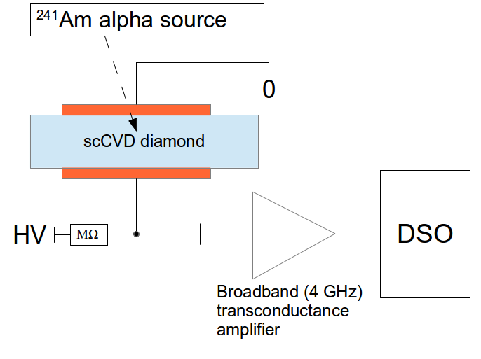
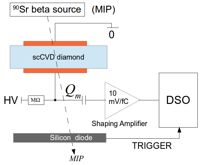
Figure 1(a) shows the setup used to perform TCT measurements. Bias voltage (with a current limiting M resistor) is provided as pull-up in the signal path. The setup is arranged so that particles enter from the opposite, grounded side of the sample. The penetration depth of in diamond is . The profile of current induced by primary e-h pairs as they traverse the bulk can be measured as a function of time.
The readout scheme for measuring the charge collection efficiency shown in Figure 1(b) is similar. A collimated source is aligned with the diamond and a trigger silicon diode. A charge shaping amplifier integrates the deposited charge and measures in the sample.
1.1 Results: current profile
| 280 K |
![[Uncaptioned image]](/html/1411.4122/assets/figures/TCT/ePlots/avgPulse_280k100V_e.png)
|
![[Uncaptioned image]](/html/1411.4122/assets/figures/TCT/hPlots/avgPulse_280k-100V_h.png)
|
| 210 K |
![[Uncaptioned image]](/html/1411.4122/assets/figures/TCT/ePlots/avgPulse_210k100V_e.png)
|
![[Uncaptioned image]](/html/1411.4122/assets/figures/TCT/hPlots/avgPulse_210k-100V_h.png)
|
| 170 K |
![[Uncaptioned image]](/html/1411.4122/assets/figures/TCT/ePlots/avgPulse_170k100V_e.png)
|
![[Uncaptioned image]](/html/1411.4122/assets/figures/TCT/hPlots/avgPulse_170k-100V_h.png)
|
| 95 K |
![[Uncaptioned image]](/html/1411.4122/assets/figures/TCT/ePlots/avgPulse_95k100V_e.png)
|
![[Uncaptioned image]](/html/1411.4122/assets/figures/TCT/hPlots/avgPulse_95k-100V_h.png)
|
| 4 K |
![[Uncaptioned image]](/html/1411.4122/assets/figures/TCT/ePlots/avgPulse_4k100V_e.png)
|
![[Uncaptioned image]](/html/1411.4122/assets/figures/TCT/hPlots/avgPulse_4k-100V_h.png)
|
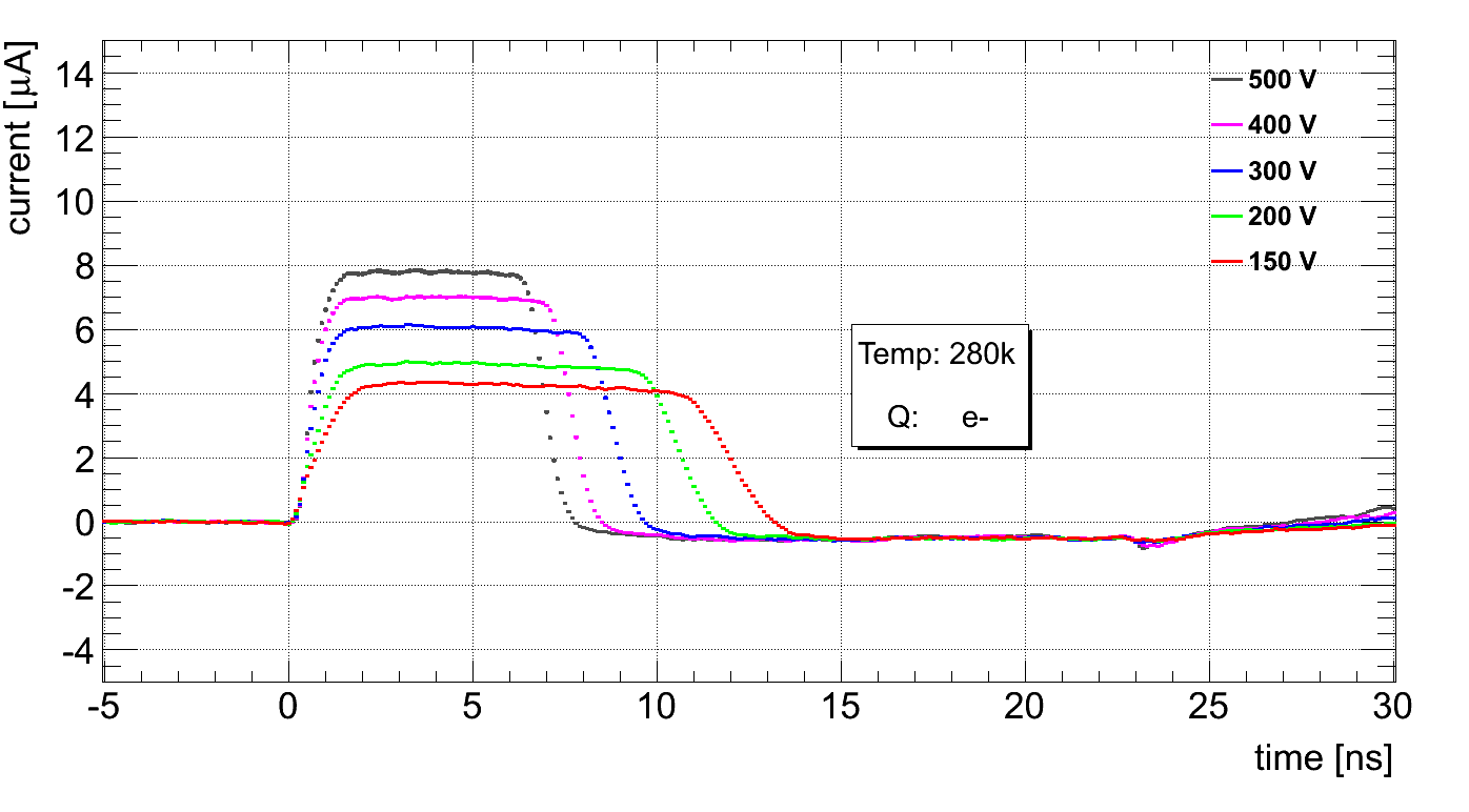
Table 2 shows results of the TCT current profile measurements as a function of bias voltage and temperature. Figure 2 highlights the results for electrons at room temperature.
The signal rises fast due to the plasma of primary e - h pairs created by the , followed by a flat phase during which charge carriers drift in the uniform electric field, inducing a constant current in the signal electrodes. There is an exponentially decaying tail when the charge carriers are collected at the electrode. At lower temperatures, there is a pronounced slope in the drift phase of the signal indicating the presence of space charge. High carrier mobility and carrier recombination in the charge cloud at low temperature[2] reduces the pulse duration and amplitude.
1.2 Comparison with TCAD calculations
We have performed TCAD calculations in the Sentaurus tool suite to cross-check our experimental measurements. A simplified geometry shown in Figure 3(a) with 300 diamond and two dimensional calculation was used to improve convergence time. With a space charge of specified in the input, the results obtained are shown in Figure 3(b).
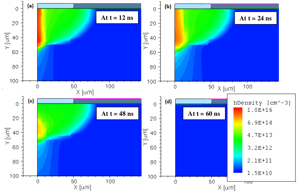
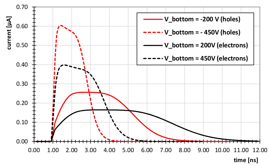
The TCAD calculation results are in qualitative agreement with the trend of the TCT measurements in Table 2 but the signal magnitude is significantly smaller. There are a few possible reasons for the discrepancy: a) in simulation, the ionizing enters into the crystal at the electrode to which high voltage is applied; b) the simplified two dimensional geometry and c) the space charge setting in the calculation. Reason (a) is most likely since we have found that in our experimental setup (Figure 1(a)) reversing the direction of the entry reduces the signal magnitude.
1.3 Results: MIP signal distribution, Charge collection efficiency
Figure 4(a) shows a characteristic Landau distribution of signals recorded from passage of minimum ionizing particles through the diamond. We have shown a comparison of signals recorded in the 2a sample and the e6 sample in the same setup.
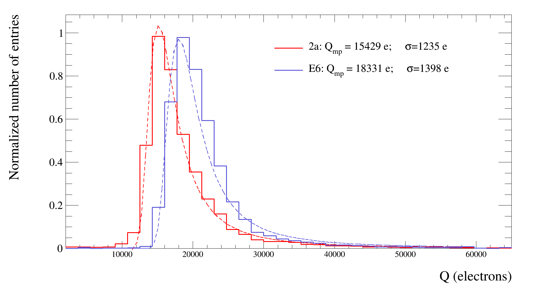
Using the benchmark figure of in diamond and sample thickness for 2a ( for e6) the Charge collection efficiency (CCE) is calculated as the ratio of the measured charge to the total charge deposited in the sample:
This also gives a measure of the charge collection distance to be in 2a and in the e6 sample.
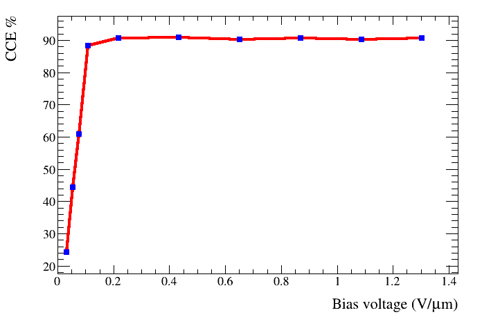
Our measurements of as a function of the bias voltage shown in Figure 4(b) indicate that the sample reaches close to maximum CCE already at 0.2V/ bias.
2 COMET: Coherent Muon to Electron detection experiment at J-PARC
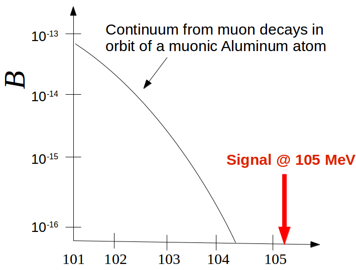
The COMET experiment at J-PARC[3] will look for physics beyond the standard model through charged lepton flavor violation (CLFV). Muons are captured in an aluminum target to create muonic atoms. After waiting for which allows for natural muon to electron decay, the experiment looks for the emission of an electron with kinetic energy exactly equal to the rest mass of the muon minus its (small) binding energy in the aluminum atom. This would indicate a coherent conversion of the muon to electron a CLFV process not allowed by the standard model. The expected signal stands out at the end of the continuum as shown in Figure 5(a). The sensitivity of the experiment is determined by the muon statistics. Hence a beam profile monitor is necessary to ensure the purity and time structure of the beam.
2.1 Radiation and timing requirements
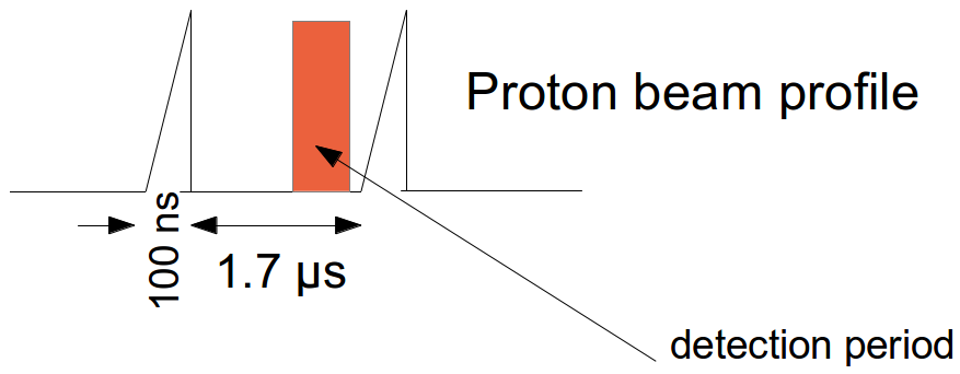
The beam structure is indicated in Figure 5(b). At startup, we expect to have an 8 GeV beam of intensity protons/sec. In stable operation, the beam intensity is ramped up to protons/sec to increase muon flux and improve the sensitivity of the experiment.
The primary challenge in monitoring the beam profile is high proton flux and the necessity to ensure that the beam is completely extinguished in 100 ns. Any stray protons entering the beamline outside the 100ns bunch would contribute to background during the detection period highlighted in red in Figure 5(b). The combination of high radiation dose and fast timing make diamond an ideal choice for this application.

Figure 6 shows the COMET experimental setup. An 8 GeV proton beam is slow-extracted from J-PARC in 100 ns bunches. The protons create pions in a stopping target. Pions decay in flight to muons. The aluminum muon capture target is placed at the end of the beamline.
3 Conclusions
We have measured signal properties and charge collection efficiency in scCVD diamond from a new vendor 2a systems. The TCT current response is excellent at 5 ns signal fwhm with no indication of space charge at room temperature, i.e. absence of any charge trapping centers. The charge collection efficiency in a our 460 sample at 1 bias is 92.9%. Both these properties combined with the high radiation tolerance (to be studied) make this scCVD diamond an excellent choice to construct a beam profile monitor for the COMET experiment at J-PARC.
Acknowledgements.
We are grateful to the following for help and support: 2a Systems, Singapore for providing the scCVD diamond; Cividec GmbH for the readout amplifiers, CERN PH-ADE-ID and the CERN CRG group for access to cryogenic test facilities, IIT Bombay Industrial Research and Consultancy Center (MHRD, Government of India) for travel support and IIT Bombay Department of Electrical Engineering, for access to Sentaurus TCAD.References
-
[1]
H. Pernegger, S. Roe, P. Weilhammer, V. Eremin, H. Frais-Klbl, E. Griesmayer,
H. Kagan, S. Schnetzer, R. Stone, W. Trischuk, D. Twitchen, A. Whitehead,
Charge-carrier properties in synthetic single-crystal diamond measured
with the transient-current technique
J. Appl. Physics 97 (7) (2005) 073704. -
[2]
H. Jansen, D. Dobos, T. Eisel, H. Pernegger, V. Eremin and Norbert Wermes,
Temperature dependence of charge carrier mobility in single-crystal
chemical vapour deposition diamond
J. Appl. Physics 113 (2013) 173706. -
[3]
Y. Kuno on behalf of the COMET collaboration,
A sarch for muon-to-electron conversion at J-PARC: the COMET experiment
Prog. Theor. Exp. Phys. (2013) 022C01.