]scalari@phys.ethz.ch
High quality factor, fully switchable THz superconducting metasurface
Abstract
We present a complementary THz metasurface realised with Niobium thin film which displays a quality factor Q=54 and a fully switchable behaviour as a function of the temperature. The switching behaviour and the high quality factor are due to a careful design of the metasurface aimed at maximising the ohmic losses when the Nb is above the critical temperature and minimising the radiative coupling. The superconductor allows the operation of the cavity with an high Q and inductive elements with an high aspect ratio. Comparison with three dimensional finite element simulations highlights the crucial role of the inductive elements and of the kinetic inductance of the Cooper pairs in achieving the high quality factor and the high field enhancement.
Metamaterials Pendry et al. (1999); Schurig et al. (2006); Chen et al. (2006) proved in the last 15 years to be an extremely flexible and useful concept Engheta (2007) that has been implemented in many different contexts, from fundamental research Papasimakis et al. (2008) to applications Lee et al. (2014). The possibility to engineer the electromagnetic response of surfaces and materials Cai et al. (2007) with 2D Luk’yanchuk et al. (2010) and 3D structures Gansel et al. (2009); Paulillo et al. (2014); Fan et al. (2011) with constitutive elements much smaller than the wavelength has opened new and exciting possibilities, from integrated optics N.Yu et al. (2011) to solid state physics Liu et al. (2012) and strong light-matter couplingScalari et al. (2012), just to name a few.
Recently, we reported on experiments on ultrastrong light-matter coupling at THz frequencies with superconducting Niobium (Nb) metasurfaces Scalari et al. (2014). In order to address theoretical predictions on peculiar cavity QED effects which arise in such ultrastrong coupling regime Ciuti, Bastard, and Carusotto (2005); Ridolfo, Savasta, and Hartmann (2013); Ridolfo et al. (2011); Stassi et al. (2013), it is necessary to be able to perform non-adiabatic experiments at THz frequencies. Superconducting metamaterials have been investigated in the THz Ricci, Orloff, and Anlage (2005); Jin et al. (2010); Zhang et al. (2012); Chen et al. (2010); Anlage (2011) and superconductors (SC) indeed display transition times of the order of the ps Singh et al. (2012); Matsunaga and Shimano (2012) when illuminated with high intensity, ultrafast optical pulses. The objective of our study is the realisation of a metasurface operating in the THz with high quality factor and displaying a pronounced switching behaviour. We would like to achieve a metasurface that displays a two-state behaviour: a narrow band, high transmission in the range 200-400 GHz (well below the Nb gap frequency of 730 GHz) that can be commuted to a broadband, low transmission. At the same time, since we are interested in cavity QED at THz frequencies Scalari et al. (2012), we aim at realising a meta-atom which provides a very small mode volume, in order to enhance the vacuum field fluctuations that scale as where is the cavity mode volume, is the photon angular frequency and where neff is the effective refractive index Devoret, Girvin, and Schoelkopf (2007). The same high ratio will lead to an high field enhancement factor.
Switchable metasurfaces have been presented in literature, by using composite metamaterials structures Chen et al. (2008) or by employing BCS or high Tc superconductors Jin et al. (2010); Zhang et al. (2012); Chen et al. (2010); Singh et al. (2013). Q factors of these structures were in the range of 5-15, and in some cases Chen et al. (2010); Singh et al. (2013) the resonance was efficiently quenched for temperature values above Tc. In our previous structures Scalari et al. (2014), we obtained a switching ratio between 3 K and 10 K with a non-optimised structure.
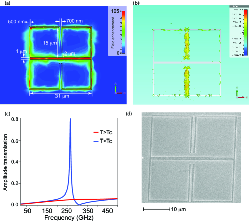
In the present study we used Nb as a superconducting material and we designed the cavity to be resonant around 250 GHz. In order to maximise the switching effect due to the presence of the superconducting state, we adopted the following design strategy: we increased the radiative Q factor in order to have a structure whose resonance line width is not radiatively limited but loss limited. Then, as a second step, we engineered the inductive elements using a very high aspect ratio (l length and A cross section)in order to maximise the losses when the structure is in the normal state. At the same time these elements will contribute negligibly to the losses when the Nb is superconducting. The resonator design is reported in Fig.1 together with 3D simulations of the electric field distribution, the surface currents, the simulated amplitude transmission and an SEM picture of the fabricated metasurface. The radiative quality factor can be engineered by acting on the capacitor gap dimension in order to reduce the efficiency of the dipolar coupling as well as the inter-meta-atom spacing Singh, Rockstuhl, and W.Zhang (2010). When designing the structure we then identified the regions of the resonator were the highest current density is flowing (see Fig.1(b)) , which will give rise to the higher ohmic losses. We then engineered such regions in order to maximize the effect of the superconducting transition. By employing very narrow (700 nm) and long (13 m) inductive elements we obtain a very high resistance when the superconductor is above Tc (for our film K Scalari et al. (2014)). On the contrary, when the Nb is operated below Tc, such regions present an higher inductance due to the kinetic inductance of the Cooper pairs and their loss is reduced by the very low, close to zero, value of the real part of the surface impedance.
In order to simulate the structure we employed a surface impedance model as reported in Refs Chen et al. (2010); Scalari et al. (2014). The surface impedance values for the Nb have been measured in our previous study Scalari et al. (2014). The detailed geometry of the meta-atom is reported in Fig.1(a) and in the caption. From the simulations of Fig.1(a) we can see that we obtain an high field enhancement factor of about 100 at resonance and from the predicted amplitude transmission curves (Fig.1(c)) we can see that the designed metasurface provides the searched switchable behaviour. The metasurface is fabricated with Electron-Beam lithography and Reactive Ion Etching on a 100 nm thick Nb film following the same procedure reported in Scalari et al. (2014): an SEM micrograph of the fabricated sample is visible in Fig.1(d).
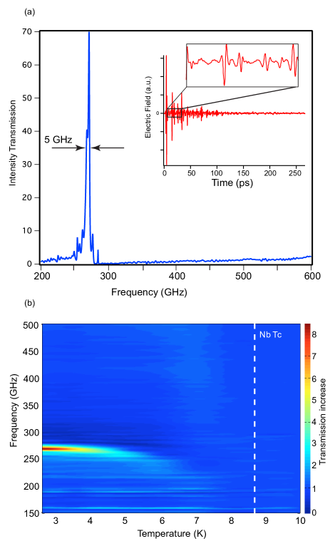
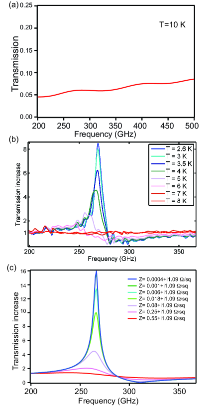
Measurements are performed with a THz-TDS system (described in RefScalari et al. (2012) ) coupled to a bath cryostat where we can vary the temperature of the sample between 2.6 K and 300 K. In Fig. 2(a) we report the transmission spectrum for the metasurface at the lowest temperature T=2.6 K. The normalisation of the the transmission is made using the high temperature (10 K) transmission of the metasurface, when the Nb is fully in the normal state an shows no resonance (see Fig.3(a)). This allows to perform a high resolution measurement reducing the interference fringes due to multiple reflections of the THz pulses inside the sample. The measured quality factor at T=2.6 K is Q=54, which compares well with results obtained on other superconductor metamaterials Jin et al. (2010); Zhang et al. (2012); Chen et al. (2010) and is comparable with the best results on metamaterials employing interference phenomena W.Cao et al. (2007). The structure displays a very narrow transmission resonance peaked at 269 GHz for the lowest temperature. When the sample is heated the transmission resonance broadens and redshifts and finally disappears for temperatures above 8 K (see Fig.3(a)). This behaviour can be appreciated by looking at the colour plot of Fig. 2(b). The observed behaviour as a function of the temperature is qualitatively well reproduced by the simulations reported in Fig.3(c).
As it clear from simulations and measurements, the design of the metasurface was optimised as well with respect to the symmetry and the shape of the resonance. In other high-Q design approaches based on inter-meta atoms coupling, interference phenomena and Fano-like couplingW.Cao et al. (2007); Luk’yanchuk et al. (2010); Papasimakis et al. (2008); Tassin et al. (2009); Gu et al. (2012) the line shape of the high Q mode is,by construction, frequently complex and spectrally very close to other broader resonances. If employed in cavity QED experiments, this kind of line shape could result in complex spectra which would be not so easy to interpret.
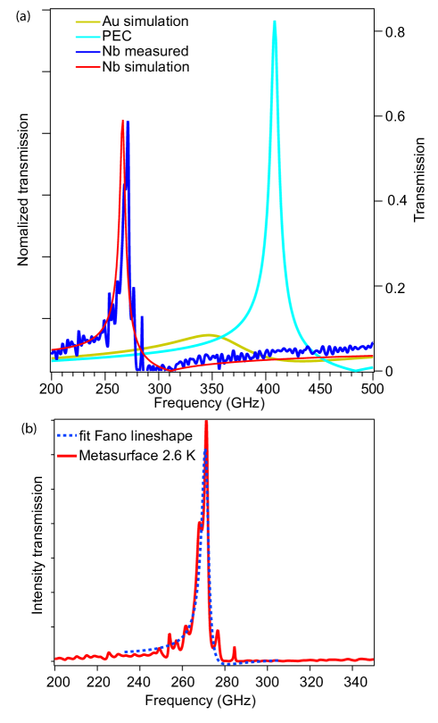
We now want to analyze the behaviour of the structure using finite element simulations performed with CST microwave studio. We performed simulations employing Nb, Au and Perfect Electric Conductor (PEC) as materials for the metasurface. The Gold has been also simulated with the surface impedance method in order to be fully comparable with the Nb. The results of such simulations are reported in Fig. 4(a). The PEC simulation allows us to disentangle the roles of the radiative quality factor Qrad and of the loss quality factor Qloss. Since PEC does not present any material loss the quality factor of the structure in this case represents the radiative coupling and is equal to Q.
The high radiative quality factor in this kind of electronic split ring resonator is the result of our optimised design for a low loss conductor. We chose the symmetric, electronic-like Schurig, Mock, and Smith (2006) split ring resonator approach in order to control the radiative coupling mainly with the capacitor gap and its width. Due to its symmetry, the coupling to the resonator through magnetic field is negligible and the coupling happens at first order through the capacitor. By adopting a narrow (1 m gap ) capacitor we can increase the radiative quality factor and target a fairly low frequency using long inductors. The use of long inductive elements would be penalising because of the high ohmic loss, but in our case we employ a superconductor so we keep these losses at the minimum. The relation which expresses the total quality factor for a resonator as a function of material loss and radiation loss is:
| (1) |
We can then use the simulated value of the quality factor for the PEC to deduce the loss quality factor for the measured Nb and the simulated Au. All the results are reported in Tab.1 I. The resonator we propose, if fabricated with Gold, presents a very low loss quality factor due to the narrow and long wires that result highly dissipative even when fabricated with a good conductor. On the contrary, the Nb resonator displays a high loss quality factor when in the superconducting state due to the low value of the real part of the surface impedance and the high value of the reactance.
It is important to highlight the narrow temperature range ( K) over which the switching of the overall Q factor of the resonator occurs, compared to other results reported in literature for high Tc superconductors Chen et al. (2010); Singh et al. (2013).
It is interesting to note also the important contribution of the kinetic inductance of the superconducting phase to determine the correct frequency of the resonator. If we examine again Table I we see that for a perfect electric conductor with no kinetic inductance the resonant frequency is GHz which is 1.5 times of what obtained with the Nb. This highlights the role of the term in the expression for the resonance frequency of the superconducting metasurface below Tc expressed as:
| (2) |
where is the geometric inductance and C the capacitance of the LC circuit associated to the meta-atom. The kinetic inductance for a superconducting wire of length and cross sectional area can be written as :
| (3) |
where is the Cooper pair density and m the electron mass. We already pointed out that we chose inductances with a very high aspect ratio in order to maximise the resistance when . The same aspect ratio enhances the kinetic inductance role in the determination of the resonator frequency.
| Nb Theo | Nb exp | Au theo | PEC | |
|---|---|---|---|---|
| (GHz) | 266 | 269 | 346 | 408 |
| Qtot | 53 | 54 | 5 | 62 |
| Qrad | 62 | 62 | 62 | 62 |
| Qloss | 405 | 418 | 5.4 |
In the case of Gold and PEC the kinetic term is very small or absent Singh et al. (2013) and the resulting resonator frequency is much higher. This fact has a strong impact when considering the field enhancement factor and the vacuum field fluctuation for a cavity at a given frequency. The lowering of the ohmic loss introduced by the PEC condition allows to have a high Qloss but is the presence of the high kinetic inductance term of the Cooper pairs which leads to a very favourable frequency-to-volume ratio.
The split-ring resonator cavity, whose dimensions are already strongly sub wavelength, is now yielding a much lower frequency because of the kinetic inductance contribution which lowers the frequency according to Eq. 2 and as visible from the simulation values in Table I. In order to obtain such a low frequency with a normal conductor, we should have rescaled the resonator with bigger dimensions, then lowering the ratio : the kinetic inductance is instrumental in obtaining a more compact resonator Anlage (2011). From our 3D simulations we deduce a field enhancement of at GHz for the superconducting resonator (see Fig.1(a)).
If one inspects the line shape of the metasurface resonance it is evident a slight asymmetry with a steeper slope on the blue side. In Figure 4(b) we plot again the intensity transmission for the metasurface at 2.6 K together with the fit employing a Fano intensity line shape Luk’yanchuk et al. (2010). The good agreement of the fit with the data (Fano coefficient f=0.19, GHz) reveals the underlying Fano coupling between the low Q, highly spatially delocalised weak transmission of the array and the high Q, LC resonance of our complementary split-ring cavities.
In conclusion, we demonstrated a new design for a complementary superconducting cavity which presents a high switching ratio between the superconducting state, where the quality factor of the resonance is as high as 54, and the normal state where the resonance is absent. The role of the kinetic inductance and of the high aspect ratio inductive element is elucidated with measurements and finite element simulations. This kind of cavity can be applied in cavity quantum electrodynamics at THz frequencies and as a narrow band switchable filter.
We acknowledge financial support from the Swiss National Science Foundation (SNF) through the National Centre of Competence in Research Quantum Science and Technology and through the SNF grant n. 129823. We also acknowledge financial support from the ERC grant MUSIC. We would like to thank J. Keller for help with measurements and F. Valmorra for the careful reading of the manuscript.
References
- Pendry et al. (1999) J. B. Pendry, A. J. Holden, D. J. Robbins, and W. J. Stewart, “Magnetism from conductors and enhanced nonlinear phenomena,” IEEE Trans. Microwave Th. Tech 47, 2075 (1999).
- Schurig et al. (2006) D. Schurig, J. J. Mock, B. J. Justice, S. A. Cummer, J. B. Pendry, A. F. Starr, and D. R. Smith, “Metamaterial electromagnetic cloak at microwave frequencies,” Science 314, 977–980 (2006).
- Chen et al. (2006) H.-T. Chen, W. J. Padilla, J. Zide, A. Gossard, A. Taylor, and R. Averitt., “Active terahertz metamaterial devices,” Nature 444, 597 (2006).
- Engheta (2007) N. Engheta, “Circuits with light at nanoscales: Optical nanocircuits inspired by metamaterials,” Science 317, 1698 (2007).
- Papasimakis et al. (2008) N. Papasimakis, V. A. Fedotov, N. I. Zheludev, and S. L. Prosvirnin, “Metamaterial analog of electromagnetically induced transparency,” Phys. Rev. Lett. 101, 253903 (2008).
- Lee et al. (2014) J. Lee, M. Tymchenko, C. Argyropoulos, P. Y. Chen, F. Lu, F. Demmerle, G. Boehm, M. C. Amann, A. Alu, and M. Belkin, “Giant nonlinear response from plasmonic metasurfaces coupled to intersubband transitions,” Nature 511, 65 (2014).
- Cai et al. (2007) W. Cai, U. Chettiar, A. Kildishev, and V. Shalaev, “Optical cloaking with metamaterials,” Nature Photonics 1, 224 (2007).
- Luk’yanchuk et al. (2010) B. Luk’yanchuk, N. Zheludev, S. A. Maier, N. Halas, P. Nordlander, H. Giessen, and C. Chong, “The fano resonance in plasmonic nanostructures and metamaterials,” Nature Materials 9, 707 (2010).
- Gansel et al. (2009) J. Gansel, M. Thiel, M. Rill, M. Decker, K. Bade, V. Saile, G. von Freymann, S. Linden, and M. Wegener, “Gold helix photonic metamaterial as broadband circular polarizer,” Science 325, 1513 (2009).
- Paulillo et al. (2014) B. Paulillo, J. Manceau, A. Degiron, N. Zerounian, G. Beaudoin, I. Sagnes, and R. Colombelli, “Circuit-tunable sub-wavelength thz resonators: hybridizing optical cavities and loop antennas,” Optics Express 22, 21302 (2014).
- Fan et al. (2011) K. Fan, A. C. Strikwerda, H. Tao, X. Zhang, and R. Averitt, “Stand-up magnetic metamaterials at terahertz frequencies,” Optics Express 19, 12619 (2011).
- N.Yu et al. (2011) N.Yu, P. Genevet, M. Kats, F. Aieta, J.-P. Tetienne, F. Capasso, and Z. Gaburro, “Light propagation with phase discontinuities: Generalized laws of reflection and refraction,” Science 334, 333 (2011).
- Liu et al. (2012) M. Liu, H. Y. Hwang, H. Tao, A. C. Strikwerda, K. Fan, G. R. Keiser, A. J. Sternbach, K. G. West, S. Kittiwatanakul, J. Lu, S. Wolf, F. G. Omenetto, X. Zhang, K. A. Nelson, and R. Averitt, “Terahertz-field-induced insulator-to-metal transition in vanadium dioxide metamaterial,” Nature 487, 345 (2012).
- Scalari et al. (2012) G. Scalari, C. Maissen, D. Turcinkova, D.Hagenmuller, S. Liberato, C. Ciuti, C. Reichl, D. Schuh, W. Wegscheider, M. Beck, and J. Faist, “Ultrastrong coupling of the cyclotron transition of a two-dimensional electron gas to a thz metamaterial,” Science 335, 1323 (2012).
- Scalari et al. (2014) G. Scalari, C. Maissen, S.Cibella, R. Leoni, P. Carelli, F. Valmorra, M. Beck, and J. Faist, “Superconducting complementary metasurfaces for thz ultrastrong light-matter coupling,” New Journ. Phys. 16, 033005 (2014).
- Ciuti, Bastard, and Carusotto (2005) C. Ciuti, G. Bastard, and I. Carusotto, “Quantum vacuum properties of the intersubband cavity polariton field ,” Phys. Rev. B 72, 115303–1–115303–9 (2005).
- Ridolfo, Savasta, and Hartmann (2013) A. Ridolfo, S. Savasta, and M. J. Hartmann, “Nonclassical radiation from thermal cavities in the ultrastrong coupling regime,” Phys. Rev. Lett. 110, 163601 (2013).
- Ridolfo et al. (2011) A. Ridolfo, R. Vilardi, O. D. Stefano, S. Portolan, and S. Savasta, “All optical switch of vacuum rabi oscillations: The ultrafast quantum eraser,” Phys. Rev. Lett. 106, 013601 (2011).
- Stassi et al. (2013) R. Stassi, A. Ridolfo, O. D. Stefano, M. J. Hartmann, and S. Savasta, “Spontaneous conversion from virtual to real photons in the ultrastrong-coupling regime,” Phys. Rev. Lett. 110, 243601 (2013).
- Ricci, Orloff, and Anlage (2005) M. Ricci, N. Orloff, and S. M. Anlage, “Superconducting metamaterials,” Appl. Phys. Lett. 87, 034102 (2005).
- Jin et al. (2010) B. Jin, C. Zhang, S. Engelbrecht, A. Pimenov, J. Wu, Q. Xu, C. Cao, J. Chen, W. Xu, L. Kang, and P. Wu, “Low loss and magnetic field-tunable superconducting terahertz metamaterial,” Optics Express 18, 17504–17509 (2010).
- Zhang et al. (2012) C. H. Zhang, J. B. Wu, B. B. Jin, Z. M. Ji, L. Kang, W. W. Xu, J. Chen, M. Tonouchi, and P. H. Wu, “Low-loss terahertz metamaterial from superconducting niobium nitride films,” Optics Express 20, 42–47 (2012).
- Chen et al. (2010) H.-T. Chen, H. Yang, R. Singh, J. F. O Hara, A. K. Azad, S. A. Trugman, and a. A. J. T. Q. X. Jia, “Tuning the resonance in high-temperature superconducting terahertz metamaterials,” Phys. Rev. Lett. 105, 247402 (2010).
- Anlage (2011) S. Anlage, “The physics and applications of superconducting metamaterials,” J. Opt. 13, 024001 (2011).
- Singh et al. (2012) R. Singh, J.Xiong, A. Azad, H. Yang, S. A. Trugman, Q. X. Jia, A. J. Taylor, and H. Chen, “Optical tuning and ultrafast dynamics of high-temperature superconducting terahertz metamaterials,” Nanophotonics 1, 117 (2012).
- Matsunaga and Shimano (2012) R. Matsunaga and R. Shimano, “Nonequilibrium bcs state dynamics induced by intense terahertz pulses in a superconducting nbn film,” Phys. Rev. Lett. 109, 187002 (2012).
- Devoret, Girvin, and Schoelkopf (2007) M. H. Devoret, S. M. Girvin, and R. J. Schoelkopf, “Circuit-qed: How strong can the coupling between a josephson junction atom and a transmission line resonator be?” Annalen der Physik 16, 767 (2007).
- Chen et al. (2008) H. Chen, J. O’Hara, A. Azad, A. Taylor, R. Averitt, D. Shrekenhamer, and W. Padilla, “Experimental demonstration of frequency-agile terahertz metamaterials,” Nature Phot. 2, 295 (2008).
- Singh et al. (2013) R. Singh, Dibakar, R. Chowdhury, J. Xiong, H. Yang, A. Azad, A. J. Taylor, Q. X. Jia, and H. Chen, “Influence of film thickness in thz active metamaterial devices: A comparison between superconductor and metal split-ring resonators,” Appl. Phys. Lett. 103, 061117 (2013).
- Singh, Rockstuhl, and W.Zhang (2010) R. Singh, C. Rockstuhl, and W.Zhang, “Strong influence of packing density in terahertz metamaterials,” Appl. Phys. Lett. 97, 241108–1–241108–3 (2010).
- W.Cao et al. (2007) W.Cao, R. Singh, I. I. Al-Naib, M. He, A. Taylor, and W. Zhang, “Low-loss ultra-high-q dark mode plasmonic fano metamaterials,” Optics Letters 16, 3366 (2007).
- Tassin et al. (2009) P. Tassin, L. Zhang, T. Koschny, E. N. Economou, and C. M. Soukoulis, “Low-loss metamaterials based on classical electromagnetically induced transparency,” Phys. Rev. Lett. 102, 053901 (2009).
- Gu et al. (2012) J. Gu, R. Singh, X. Liu, X. Zhang, Y. Ma, S. Zhang, S. Maier, Z. Tian, A. K. Azad, H. Chen, A. Taylor, J. Han, and W. Zhang, “Active control of electromagnetically induced transparency analogue in terahertz metamaterials,” Nature Communications 3, 1151 (2012).
- Schurig, Mock, and Smith (2006) D. Schurig, J. J. Mock, and D. R. Smith, “Electric-field-coupled resonators for negative permittivity metamaterials,” Appl. Phys. Lett. 88, 041109 (2006).