Indirect band gap in graphene from modulation of the Fermi velocity
Abstract
In this work we study theoretically the electronic properties of a sheet of graphene grown on a periodic heterostructure substrate. We write an effective Dirac equation, which includes a dependence of both the band gap and the Fermi velocity on the position, due to the influence of the substrate. This way, both bandgap and Fermi velocity enter the Dirac equation as operators. The Dirac equation is solved exactly and we find the superlattice minibands with gaps due to the breaking of translational symmetry induced by the underlying heterostructure. The spatial dependence of the Fermi velocity makes the band gap be indirect, bringing about interesting possibilities for applications in the design of nanoelectronic devices. In the limit of constant Fermi velocity we obtain a band structure, with direct band gap, very close to the one previously found in the literature, obtained using the transfer matrix method.
keywords:
1 Introduction
Most semiconductor devices presently being developed and produced have two or more kinds of semiconductor materials composing, what is called a heterostructure [1]. The variation of the composition is used to control fundamental parameters in semiconductor crystals and devices, such as the motion of electrons and holes, the effective mass of charge carriers, and the electron energy spectrum, through band engineering. One important feature of heterostructures is the possibility of restricting the movement of charge carriers, creating quantum confinement. Examples of confining heterostructures are quantum dots, quantum wires and quantum wells. Transport properties of a semiconductor may be obtained using the effective mass theory [2, 3, 4]. In this approach, electrons (or holes) are described as free particles with an effective mass that incorporates the interaction between the carriers and the lattice structure. Since the effective mass of the carriers depends on the material, in a heterostructure it depends on their position. The effective mass is then an operator which does not commute with momentum implying that the usual kinetic operator is not Hermitian and have to be modified. Effective mass operators have been largely used to obtain the minibands associated with periodicity of heterostructures [5, 6, 7, 8, 9, 10, 11].
Since its first successful experimental fabrication in 2004 [12], graphene has attracted a great deal of attention due to its interesting properties and the wide range of application. Graphene is an atomically thin layer made out of carbon atoms arranged in a hexagonal structure which presents an extremely efficient electronic conductivity with an easy control, which makes it a material with a great application potential for the fabrication of electronic devices. However, the physics of low-energy carriers in graphene is described by an effective Dirac Hamiltonian. There is no gap in the band structure of the ideal graphene sheet, so the Dirac electron becomes massless and cannot be confined by an electrostatic potential due to the Klein tunneling [13], which impedes its use in electronic devices. Nevertheless, it was shown that it is possible to suppress the Klein tunneling with a magnetic field [14, 15] and with a spatially modulated gap [16, 17], leading to confined states. For a recent review on the various possible ways to avoid Klein tunneling in graphene see reference [18].
A periodic modulation of the band gap of graphene leads to graphene-based superlattices. Recently, graphene has been successfully used in heterostructures for making atomically thin circuitry [19], high-responsivity photodetectors [20] and field-effect transistors [21], among other high-technology applications. Superlattice structures based on graphene have been studied in many forms: modulation of the gap by an externally applied periodic potential [22], alternating graphene and h-BN nanoribbons [23], alternating graphene and graphane nanoribbons [24], among others. In this work we study a heterostructure solely made of graphene, without doping and without material discontinuities. This is done by taking advantage of the influence that the substrate has on graphene. Our aim is to study the combined effects of spatial modulation of both the gap and the Fermi velocity. For this, we choose the substrate studied in reference [25] which considered the bandgap variation but not the Fermi velocity dependence on the position.
It is very well know that the electronic structure of graphene is affected by its substrate. For instance, a hexagonal boron nitride (h-BN) substrate leads to the opening of a gap of the order of meV which depends on the commensurability between the lattices [26, 27], while SiC induces a gap of eV in graphene [28]. Graphene deposited on a SiO2 surface has a gap of eV for an oxygen-terminated surface, whereas there is no band gap when the oxygen atoms are passivated with hydrogen atoms [29]. It is also on the SiO2 substrate where graphene shows the lowest quality properts, exhibiting characteristics that are very inferior to the expected in intrinsic graphene [30, 31, 32]. Recently, it was pointed out that graphene on h-BN substrate probably elastically deforms itself in order to reduce the lattice mismatch between the two structures [33]. This strain induced by the substrate has important consequences on the electronic properts of graphene [34]. Another important electronic property of graphene that depends on the substrate is the Fermi velocity. For graphene on different substrates the Fermi velocity has been measured by different authors and their results summarized in [35].
Taking advantage of the influence of the substrate on the electronic properties of graphene, P. V. Ratnikov [25] in 2009 proposed a method to spatially modulate the band gap of graphene by considering a pristine graphene sheet on a heterostructured substrate composed by alternating h-BN and SiO2 strips. Developments of this idea have appeared in the recent literature [36, 37, 38, 39] with and without a modulated externally applied field. In all these papers it was considered that the heterostructured substrate induces only an energy gap modulation, and the remaining effects of the substrate on graphene were not taken into account. However, this description was able to elucidate the effects of the energy gap modulation on the electronic structure of graphene. One of the effects neglected in these papers is the variation of the Fermi velocity. The importance of the Fermi velocity variation has been pointed out in the literature [36] but only in two cases incorporated in the study of graphene-based superlattices: the case of a bilayer [40] and the case of scattering across a heterostructure in the monolayer [16]. To the best of our knowledge, ours is the first work to present a study of the band structure of the graphene superlattice induced by the sustrate, including both modulation of the band gap and Fermi velocity. We will see below that this dependence of the Fermi velocity on the substrate leads to a direct to indirect band gap transition in graphene. We also find that the shape of the minibands is quite sensitive to the inclusion of the spatial variation of the Fermi velocity. In our study, for the sake of comparison, we use the same parameter values as in [25], including the h-BN induced bandgap of 53 meV in graphene even though more recent works [26, 27] indicate not only a lower value but also a dependence on the relative position between the graphene and the h-BN lattices.
In this work we consider a graphene sheet deposited in a heterostructured substrate composed of two different materials. We consider that in the graphene layer there will be a jump in the Fermi velocity and in the band gap at the positions corresponding to the junctions between the materials composing the substrate. We use an effective Dirac equation with position dependent gap term (mass) and Fermi velocity, which describes the low-energy states in graphene. By exactly solving the Dirac equation we find the superlattice minibands induced by the substrate heterostructure. We compare our results with the previous one [25], where the Dirac equation with a periodically modulated band gap was solved using the transfer matrix method. In our work we include the spatial variation of the Fermi velocity, which will induce an indirect band gap transition in graphene. An indirect band gap has been realized in graphene nanoribbons [41], in graphene bylayers under field modulation [42], in a graphene-graphane superlattice [24] and in a single-layer graphene sheet with combined electric and magnetic fields [43]. To the best of our knowledge, what we present here is the first case of Fermi velocity modulation yielding an indirect gap for a pristine single layer of graphene. Modulation of the Fermi velocity for a graphene bilayer was done in reference[40], which also lead to indirect gaps. We remark that there are other important effects of the substrate that we are not considering here as, for example, the effect of the strain on the graphene lattice caused by the substrate. However, this is justified since the aim of this work is to elucidate the effect of a variable Fermi velocity on graphene and compare two methods of calculating the dispersion relation. The incorporation of further substract influence on graphene will enrich the model and will be the subject of a future publication.
The paper is organized as follows. In Section II we write out the effective Dirac equation for low energy electronic states in graphene with a variable mass term, which means the energy gap, and Fermi velocity, taking into account that the Hamiltonian has to be Hermitian. In Section III we use the effective Dirac equation to find the superlattice miniband structure of graphene on the heterostructured substrate. The paper is summarized in the conclusions.
2 Effective Dirac Equation with variable gap term and Fermi velocity
We start by generalizing the two-dimensional effective Dirac equation for low-energy states in graphene for the case where the Fermi velocity and gap term depend on the position. Naively, we write
| (1) |
where are the Pauli matrices acting in the two graphene sublattices, is the Fermi velocity, is the gap term and the spinor
| (2) |
with and representing the two polarizations of the pseudospin that correspond to the graphene sublattices.
Since the Fermi velocity and the gap term both depend on position, they are operators. Furthermore, they do not commute with the linear momentum, which make the Hamiltonian non-Hermitian. To fix this, a generalization of the Dirac Hamiltonian with spatial dependent Fermi velocity was obtained from an effective low-energy theory of a tight binding model in [16], which is equivalent to consider the permutations between the operators in the first term of the Dirac operator. This way, Eq. (1) becomes
| (3) |
Notice that for we recover Eq. (1) of reference [25] with the potential .
| (5) |
and
| (6) |
Uncoupling these equations one gets
| (7) |
and
| (8) |
Before going to the next section, where we will use the uncoupled Eqs.(7) and (8) to find the band structure of the graphene superlattice, we take a look at their symmetries. It is easily seen that, by simultaneously making and the Eqs. (7) and (8) are transformed into each other. As it will be seen below this has important consequences in the type (direct or indirect) of the band gap.
3 The Superlattice Minibands
In this section, we use the effective Dirac Hamiltonian obtained in the last section to describe electrons in a graphene layer on a periodic heterostructure substrate. In an ordinary semiconductor heterostructure the charge carriers may be described as free Schrödinger electrons (or holes) with an effective mass [2, 3, 4] that depends on the material and, therefore, on position. This approach has been largely used to obtain the minibands associated with periodicity of the heterostructure (see for example [5] and references therein). In our case, we have an effective Dirac operator with both gap term and Fermi velocity depending on position to account for the substrate influence on the graphene layer.
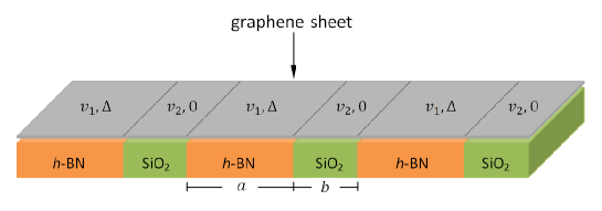
We consider a graphene sheet deposited on a periodic heterostructure substrate composed by h-BN and SiO2, as shown in Fig. 1. This will induce a heterostructure in graphene due to the dependence of both its Fermi velocity and band gap on the substrate material.
As the Hamiltonian is periodic, the wave function satisfies the Bloch theorem, so
| (9) |
and
| (10) |
where is the Bloch wavenumber and is an integer. Due to this fact, we can reduce our problem to the unit cell [see Fig.(2)].
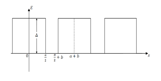
In the unit cell we have that
| (11) |
and
| (12) |
3.1 Boundary conditions
To find the band structure it is necessary to specify the boundary conditions. We already have the Bloch conditions (9) and (10), now we need the interface conditions at and (see Fig. 2). For this, we consider a general interface as shown in Fig. 3.
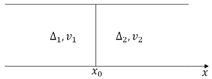
In this interface, we have
| (13) |
and
| (14) |
where is the Heaviside function.
Using the properties
| (15) |
and
| (16) |
one can write Eq. (7) as
| (17) |
Integrating from to [see Fig.3] and making , one obtains
| (18) |
In order to obtain the boundary condition for the wave function one calculates the of the Eq.(17), integrates it from to and take the limit . Following this procedure, we get for the boundary condition:
| (19) |
where
| (20) |
Analogously, for , we find
| (24) |
and
| (25) |
where
| (26) |
| (27) |
and
| (28) |
One can see that the interface conditions for are equal to the interface conditions for with the exchange of by and by .
Thus, the boundary conditions for are given by
| (29) |
| (30) |
| (31) |
| (32) |
| (33) |
and
| (34) |
where , and are equal to , and , respectively, with and . Whereas, , and are equal to , and , respectively, with , and with the exchange of by and vice-versa.
3.2 Superlattice minibands
The general solution for Eq.(7) is
| (35) |
where , , , and are constant coefficients, and .
The derivative of Eq. (35) is given by
| (36) |
Replacing the wave function (35) and its derivative (36) in the boundary conditions (29) - (34) we get a system of six equations with six coefficients. Solving them as was done in [5], we obtain the relation
| (37) | |||||
which is our main result. In this equation, , the component of the carrier wavevector, replaces the Bloch wavenumber , since in this problem they coincide.
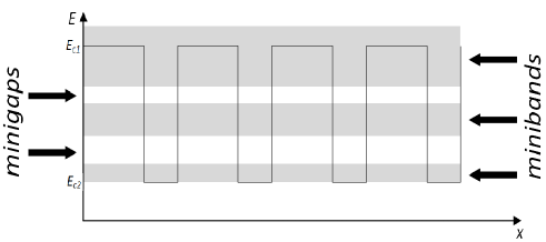
The left hand side of Eq.(37) is limited in the interval (-1,1). For this reason, in the right hand side one has forbidden values for the energy. This implies in the appearance of energy bands with gaps where initially was the conduction band. In summary, the heterostructured substrate induces a variable bandgap in graphene, as shown in Fig. 2. The periodicity of the induced properties of graphene (bandgap width and Fermi velocity) leads to the further opening of minigaps between the bottoms and of the conduction band in the differently gapped regions of the graphene sheet, as shown in Fig. 4.
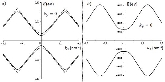
Solving for we get the same relation (37) with different coefficients which come from the interface conditions for . As mentioned previously, the boundary conditions for are equal to the boundary conditions for with the simultaneous exchange of by and by . So, the spectrum is symmetric under double reflection over both axes. This leads to an indirect band gap. When the Fermi velocity is constant, , which makes . In this case, appears in the spectrum only squared in and , so the spectrum is independently invariant under the transformation , making the band gap direct.
In Fig. 5a we compare our result for the dispersion relation (37) with that of reference [25] for , obtained using the transfer matrix method, for the same Hamiltonian. In order to do that, we made and used the same values of the lattice parameters and as in [25] . As seen in the figure, the agreement is excellent. Now, let us see the effect of considering the spatial variation of the Fermi velocity: Fig. 5b, again with , as compared to Fig. 5a shows a widening of the bandgap plus a slight flattening of the bands in the gap region.
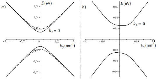
In Fig. 6a we plot the energy in terms of with . Again, to compare with reference [25] the Fermi velocity was fixed. Once again we get excellent agreement. Fig. 6b shows the case of varying Fermi velocity. Not only the gap widened but it suffered a direct to indirect transition. Here, it is clear the symmetry of the bands under reflection over both the and the axes.
4 Conclusions
We verified that modulating both the band gap and Fermi velocity in a single layer graphene sheet on a periodic substrate leads to the opening of an indirect band gap for the resulting graphene superlattice. Since a gap is of fundamental importance for electronic applications, band and Fermi velocity engineering leading to the control of both the type and width of the gap become important tools for the design of graphene-based electronic devices. We studied the specific case of graphene on alternating SiO2 and h-BN, but the model proposed here can be used in the case of a generic substrate composition. Our result was compared with the known results obtained via the transfer matrix method for constant Fermi velocity with excellent agreement.
Acknowledgements: This work was partially supported by CNPq, CNPQ-MICINN binational, CAPES-WEIZMANN binational and CAPES-NANOBIOTEC.
References
- [1] M. Dutta, M. Stroscio, Advanced Semiconductor Heterostructures: Novel Devices, Potential Device Applications and Basic Properties, Selected topics in electronics and systems, World Scientific, 2003.
- [2] G. H. Wannier, The structure of electronic excitation levels in insulating crystals, Phys. Rev. 52 (1937) 191–197.
- [3] J. C. Slater, Electrons in perturbed periodic lattices, Phys. Rev. 76 (1949) 1592–1601.
- [4] H. M. James, Electronic states in perturbed periodic systems, Phys. Rev. 76 (1949) 1611–1624.
- [5] J. R. F. Lima, M. Vieira, C. Furtado, F. Moraes, C. Filgueiras, Yet another position-dependent mass quantum model, Journal of Mathematical Physics 53 (7) (2012) 072101.
- [6] M. Gadella, F. J. H. Heras, J. Negro, L. M. Nieto, A delta well with a mass jump, Journal of Physics A: Mathematical and Theoretical 42 (46) (2009) 465207.
- [7] M. Gadella, . Kuru, J. Negro, Self-adjoint hamiltonians with a mass jump: General matching conditions, Physics Letters A 362 (4) (2007) 265 – 268.
- [8] J. Álvarez, M. Gadella, L. Nieto, A study of resonances in a one-dimensional model with singular hamiltonian and mass jumps, International Journal of Theoretical Physics 50 (7) (2011) 2161–2169.
- [9] G. T. Einevoll, P. C. Hemmer, The effective-mass hamiltonian for abrupt heterostructures, Journal of Physics C: Solid State Physics 21 (36) (1988) L1193.
- [10] R. A. Morrow, K. R. Brownstein, Model effective-mass hamiltonians for abrupt heterojunctions and the associated wave-function-matching conditions, Phys. Rev. B 30 (1984) 678–680.
- [11] G. T. Einevoll, P. C. Hemmer, J. Thomsen, Operator ordering in effective-mass theory for heterostructures. i. comparison with exact results for superlattices, quantum wells, and localized potentials, Phys. Rev. B 42 (1990) 3485–3496.
- [12] K. S. Novoselov, A. K. Geim, S. V. Morozov, D. Jiang, Y. Zhang, S. V. Dubonos, I. V. Grigorieva, A. A. Firsov, Electric field effect in atomically thin carbon films, Science 306 (5696) (2004) 666–669.
- [13] M. I. Katsnelson, K. S. Novoselov, A. K. Geim, Chiral tunnelling and the klein paradox in graphene, Nat Phys 2 (2006) 620.
- [14] G. Giavaras, P. A. Maksym, M. Roy, Magnetic field induced confinement–deconfinement transition in graphene quantum dots, Journal of Physics: Condensed Matter 21 (10) (2009) 102201.
- [15] P. A. Maksym, M. Roy, M. F. Craciun, S. Russo, M. Yamamoto, S. Tarucha, H. Aoki, Proposal for a magnetic field induced graphene dot, Journal of Physics: Conference Series 245 (1) (2010) 012030.
- [16] N. M. R. Peres, Scattering in one-dimensional heterostructures described by the dirac equation, Journal of Physics: Condensed Matter 21 (9) (2009) 095501.
- [17] G. Giavaras, F. Nori, Graphene quantum dots formed by a spatial modulation of the dirac gap, Applied Physics Letters 97 (24) (2010) –.
- [18] V. Jakubský, D. Krejčiřík, Qualitative analysis of trapped dirac fermions in graphene, Annals of Physics (0) (2014) –.
- [19] M. P. Levendorf, C.-J. Kim, L. Brown, P. Y. Huang, R. W. Havener, D. A. Muller, J. Park, Graphene and boron nitride lateral heterostructures for atomically thin circuitry, Nature 488 (2012) 627.
- [20] X. Wang, Z. Cheng, K. Xu, H. K. Tsang, J.-B. Xu, High-responsivity graphene/silicon-heterostructure waveguide photodetectors, Nat Photon 7 (11) (2013) 888–891.
- [21] J. Moon, H. chang Seo, F. Stratan, M. Antcliffe, A. Schmitz, R. Ross, A. Kiselev, V. Wheeler, L. Nyakiti, D. Gaskill, K.-M. Lee, P. Asbeck, Lateral graphene heterostructure field-effect transistor, Electron Device Letters, IEEE 34 (9) (2013) 1190–1192.
- [22] C.-H. Park, L. Yang, Y.-W. Son, M. L. Cohen, S. G. Louie, New generation of massless dirac fermions in graphene under external periodic potentials, Phys. Rev. Lett. 101 (2008) 126804.
- [23] H. Sevinçli, M. Topsakal, S. Ciraci, Superlattice structures of graphene-based armchair nanoribbons, Phys. Rev. B 78 (2008) 245402.
- [24] J.-H. Lee, J. C. Grossman, Energy gap of kronig-penney-type hydrogenated graphene superlattices, Phys. Rev. B (2011) 113413.
- [25] P. Ratnikov, Superlattice based on graphene on a strip substrate, JETP Letters 90 (6) (2009) 469–474.
-
[26]
P. San-Jose, A. Gutiérrez-Rubio, M. Sturla, F. Guinea,
Spontaneous strains
and gap in graphene on boron nitride, Phys. Rev. B 90 (2014) 075428.
doi:10.1103/PhysRevB.90.075428.
URL http://link.aps.org/doi/10.1103/PhysRevB.90.075428 -
[27]
P. San-Jose, A. Gutiérrez-Rubio, M. Sturla, F. Guinea,
Electronic
structure of spontaneously strained graphene on hexagonal boron nitride,
Phys. Rev. B 90 (2014) 115152.
doi:10.1103/PhysRevB.90.115152.
URL http://link.aps.org/doi/10.1103/PhysRevB.90.115152 - [28] S. Y. Zhou, G.-H. Gweon, A. V. Fedorov, P. N. First, W. A. de Heer, D.-H. Lee, F. Guinea, A. H. Castro Neto, A. Lanzara, Substrate-induced bandgap opening in epitaxial graphene, Nat Mater 6 (2007) 770.
- [29] P. Shemella, S. K. Nayak, Electronic structure and band-gap modulation of graphene via substrate surface chemistry, Applied Physics Letters 94 (3) (2009) 032101.
- [30] M. Ishigami, J. H. Chen, W. G. Cullen, M. S. Fuhrer, E. D. Williams, Atomic structure of graphene on sio2, Nano Letters 7 (6) (2007) 1643–1648.
- [31] S. Fratini, F. Guinea, Substrate-limited electron dynamics in graphene, Phys. Rev. B 77 (2008) 195415.
- [32] C. R. Dean, A. F. Young, I. Meric, C. Lee, L. Wang, S. Sorgenfrei, K. Watanabe, T. Taniguchi, P. Kim, K. L. Shepard, J. Hone, Boron nitride substrates for high-quality graphene electronics, Nat Nano 5 (10) (2010) 722–726.
- [33] A. Eckmann, J. Park, H. Yang, D. Elias, A. S. Mayorov, G. Yu, R. Jalil, K. S. Novoselov, R. V. Gorbachev, M. Lazzeri, A. K. Geim, C. Casiraghi, Raman fingerprint of aligned graphene/h-bn superlattices, Nano Letters 13 (11) (2013) 5242–5246.
- [34] F. de Juan, M. Sturla, M. A. H. Vozmediano, Space dependent fermi velocity in strained graphene, Phys. Rev. Lett. 108 (2012) 227205.
- [35] C. Hwang, D. A. Siegel, S.-K. Mo, W. Regan, A. Ismach, Y. Zhang, A. Zettl, A. Lanzara, Fermi velocity engineering in graphene by substrate modification, Sci. Rep. 2 (2012) 590.
- [36] G. M. Maksimova, E. S. Azarova, A. V. Telezhnikov, V. A. Burdov, Graphene superlattice with periodically modulated dirac gap, Phys. Rev. B 86 (2012) 205422.
- [37] G. Li, G. Chen, P. Peng, Z. Cao, H. Ye, Manipulation of resonant tunneling by substrate-induced inhomogeneous energy band gaps in graphene with square superlattice potentials, Physics Letters A 377 (40) (2013) 2895 – 2900.
- [38] S. Kryuchkov, E. Kukhar’, O. Nikitina, Influence of the electromagnetic wave on the transversal conductivity of the graphene superlattice, Superlattices and Microstructures 60 (0) (2013) 524 – 532.
- [39] Y. Zhang, Y. Yin, H. Zhang, Tunneling mode in symmetrical graphene superlattices with one-dimensional period potentials, The European Physical Journal Applied Physics 66.
- [40] H. Cheraghchi, F. Adinehvand, Control over band structure and tunneling in bilayer graphene induced by velocity engineering, Journal of Physics: Condensed Matter 26 (1) (2014) 015302.
- [41] K. Majumdar, K. V. R. M. Murali, N. Bhat, Y.-M. Lin, External bias dependent direct to indirect band gap transition in graphene nanoribbon, Nano Letters 10 (8) (2010) 2857–2862.
- [42] H. Raza, E. C. Kan, Field modulation in bilayer graphene band structure, Journal of Physics: Condensed Matter 21 (10) (2009) 102202.
- [43] L. Xin, W. Hai-Long, P. Hui, X. Huai-Zhe, Gap opening and tuning in single-layer graphene with combined electric and magnetic field modulation, Chinese Physics B 20 (4) (2011) 047302.