![[Uncaptioned image]](/html/1411.2768/assets/x1.png)
Alexandr E. Krasnok, Pavel A. Belov, Andrey E. Miroshnichenko, Arseniy I. Kuznetsov,
Boris S. Luk’yanchuk, Yuri S. Kivshar
Глава 0 All-dielectric optical nanoantennas
Introduction
Antennas are important elements of wireless information communication technologies, along with sources of electromagnetic radiations and their detectors. One can say that antennas are at the heart of modern radio and microwave frequency communications technologies. They are at the front-ends of satellites, cell-phones, laptops and other communicating devices. In radio engineering, antennas refer to devices converting electric and magnetic currents into radio propagating waves and, vice versa, radio waves to currents. Recently, the concept of antennas have been extended to the optical frequency domain [1, 2, 3, 4, 5, 6, 7, 8, 9]
as a result of the development of a new branch of physics emerged known as nanooptics, which studies the transmission and reception of optical signals by submicron and even nanometer-sized objects.
For nanooptics it is important to efficiently detect and direct the transmitting signals for optical information between nanoelements. The sources and detectors of radiation in nanooptics are nanoelements themselves, their clusters, and even individual molecules (atoms, ions). Nanoobjects functioning as antennas must exhibit high radiation efficiency and directivity.
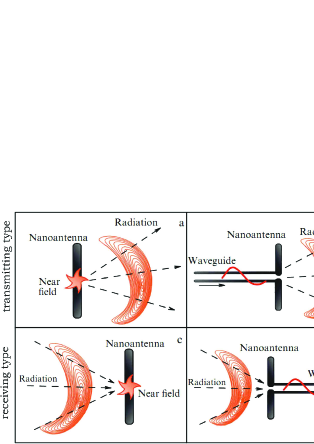
Nanoantennas, similar to the radiofrequency antennas, are usually divided into two types, transmitting and receiving (see Fig. 1). Figure 1a schematically shows the interaction between a nanoantenna and the near field of an quantum emitter. In this case, the nanoantenna transforms the near field into freely propagating optical radiation, i.e. it is a transmitting nanoantenna. Figure 1c illustrates the operation of a receiving nanoantenna that converts incident radiation into a strongly confined near field.
The energy is usually delivered to a microwave antenna through a waveguide. Such an antenna converts waveguide modes to freely propagating radiation. In the case of optical antennas with their sufficiently small optical size, the waveguide mode must have the subwavelength cross section attainable by using so-called plasmonic waveguides. This type of nanoantenna feeding is depicted schematically in Fig. 1b. According to the reciprocity principle, such a nanoantenna is also capable of transforming incident radiation to plasmonic waveguide modes (see Fig. 1d).
Thus, the transmitting antenna converts a strongly confined field in the optical frequency range created by a certain (weakly emitting or almost non emitting) source into optical radiation (see Fig. 1a,b). Conversely, the receiving nanoantenna is a device efficiently converting incident light (optical frequency radiation) into a strongly confined field (see Fig. 1c,d), where an electromagnetic field is concentrated in a small region compared to the wavelength of light. Such fields are characterized by a spatial spectrum consisting mostly of evanescent waves. The confinement region may be of subwavelength dimension, leading to a strongly confined near field. The energy of this field contains contributions from stored and non radiated energy. However, an important particular case of nanoantennas is a device converting optical radiation into waveguide modes, and vice versa, as shown in Fig. 1c,d. In this case, the subwavelength dimension is characterized by the transverse cross section of the strongly confined field region. The longitudinal size of this region (along the waveguide axis) may be optically large, and the electromagnetic energy of the strongly confined field is referred to as expanding. The feeding configuration with a plasmonic waveguide is of great importance for practical applications of nanoantennas, especially for the development of wireless communication systems at the nanometer level, i.e., for future fully optical integrated circuits.
Nanoantennas are the most promising area of research in the modern nanooptics due to their ability to bridge the size and impedance mismatch between nanoemitters and free space radiation, as well as manipulate light on the scale smaller than the wavelength of light. Bearing in mind the great variety of sources and detectors of strongly confined optical fields (groups of atoms and molecules, luminescent and fluorescent cells, e.g., viruses and bacteria, sometimes individual molecules, quantum dots, and quantum wires), it is safe to say that the areas of practical applications of nanoantennas in the near future will be commensurate with that of their classical analogs.
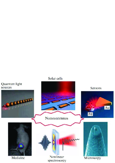
At present, nanoantennas are used in near-field microscopy and high-resolution biomedical sensors; their application for hyperthermal therapy of skin neoplasms is a matter of the foreseeable future. There are some other potential applications of nanoantennas (see Fig. 2) that we believe to be equally promising, including solar cells [10], molecular and biomedical sensors [11], optical communication [12], and optical tweezers [13]. The variety of applications allows us to argue that the concept of nanoantennas presents a unique example of the penetration of new physics into various spheres of human activity.
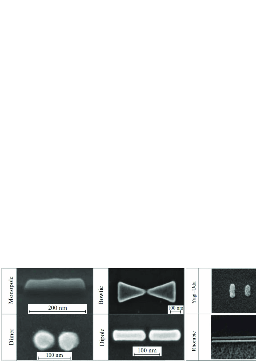
Thus far, optical antennas have primarily been constructed from metallic materials, which support plasmonic resonances. The main types of plasmonic nanoantennas which have been realized experimentally are presented in Fig. 3. Different types of plasmonic nanoantennas are designed to perform various tasks. For example dipole nanoantennas [8, 9, 14, 15, 16] demonstrate high coefficient of electric field localization, while bowtie nanoantennas [8, 9, 17, 18, 19, 20, 21, 13, 22, 23, 24] are broadband; Yagi-Uda type nanoantennas exhibit high directivity which is very useful for optical wireless communications on an optical chip [3, 8, 9, 12, 25, 26, 27, 28, 29, 30, 31, 32, 33, 34, 35]. However, despite of a number of advantages of plasmonic nanoantennas associated with their small size and strong localization of the electric field, such nanoantennas have large dissipative losses resulting in low radiation efficiency.
To overcome such limitations, we propose a new type of nanoantennas based on dielectric nanoparticles with a high index dielectric constant [36, 37, 38, 39, 9, 8, 40, 41, 42, 43, 44], for example Huygens optical elements and Yagi-Uda nanoantennas [see par.(2)]. Such all-dielectric optical nanoantennas will have low dissipative losses with enhanced magnetic response in the visible. The concept of optical magnetism based on dielectric nanoparticles is presented in the next section. The key for such novel functionalities of high index dielectric nanophotonic elements is the ability of subwavelength dielectric nanoparticles to support simultaneously both electric and magnetic resonances, which can be controlled independently. This type of nanoantennas has several unique features such as low optical losses at the nanoscale and superdirectivity. The concept of all-dielectric nanoantennas has been developed in our original papers [8, 45, 46, 40, 41, 42, 9] and also summarized below.
Furthermore all-dielectric nanoantennas allow us achieve the superdirectivity effect. Superdirectivity as a physical concept can be found in textbooks on antennas, however all so far proposed superdirective antennas are not reliably reproducible. More specifically, all previous attempts to achieve superdirectivity of antennas were based on discrete arrays of radiating dipoles with a rather cumbersome distribution of radiating currents over the array. This approach resulted in intrinsic drawbacks of known superdirective arrays - ultra-narrowfrequency range, high dissipation, and extreme sensitivity to any disturbance, etc. As a result, no single superdirective antenna was demonstrated up to now. In the context of nanoantennas, which originated from radio frequency antennas a few years ago, superdirectivity has never been discussed. However, superdirectivity would be a very desirable feature in nanophotonics with numerous useful applications. Here we describe [see par.(3)] the superdirectivity effect in a very simple, elegant, and practical way for a nanoparticle with a notch. This approach is able to shape higher-harmonics of the radiation field in such a way that not only superdirectivity of this nanoantennas becomes possible but also a strong subwavelength sensitivity of the radiation pattern to the location of the emitter can be easily realized.
1 Optical magnetism based on dielectric nanoparticles
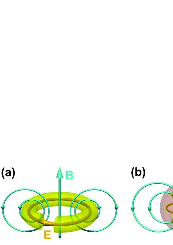
It is well known that a pair of oscillating electric charges of opposite signs, know as an oscillating electric dipole, produces electromagnetic radiation at the oscillations frequency [48]. Although, distinct “magnetic charges”, or monopoles, have not been observed so far, magnetic dipoles are very common sources of magnetic field in nature. The field of the magnetic dipole is usually calculated as the limit of a current loop shrinking to a point. Its profile is equivalent to the one of an electric dipole considering that the electric and magnetic fields are exchanged. The most common example of a magnetic dipole radiation is an electromagnetic wave produced by an excited metal split-ring resonator (SRR), which is a basic constituting element of metamaterials (see Fig. 4a) [49, 50, 51, 52, 53, 54, 55, 56, 57]. The real currents excited by external electromagnetic radiation and running inside the SRR produce a transverse oscillating up and down magnetic field in the center of the ring, which simulates an oscillating magnetic dipole. The major interest of these artificial systems is due to their ability to response to a magnetic component of incoming radiation and thus to have a non-unity or even negative magnetic permeability () at optical frequencies, which does not exist in nature. This provides possibilities to design unusual material properties such as negative refraction [49, 50, 51, 52, 53, 54, 55, 56, 57], cloaking [58, 59], or superlensing [60]. The SRR concept works very well for gigahertz [55, 56, 57], terahertz [61, 62] and even near-infrared (few hundreds THz) [63, 64, 65] frequencies. However, for shorter wavelengths and in particular for visible spectral range this concept fails due to increasing losses and technological difficulties to fabricate smaller and smaller constituting split-ring elements [64, 66]. Several other designs based on metal nanostructures have been proposed to shift the magnetic resonance wavelength to the visible spectral range [49, 50]. However, all of them are suffering from losses inherent to metals at visible frequencies.
An alternative approach to achieve strong magnetic response with low losses is to use nanoparticles made of high-refractive index dielectric materials [53, 67]. As it follows from the exact Mie solution of light scattering by a spherical particle, there is a particular parameter range where strong magnetic dipole resonance can be achieved. Remarkably, for the refractive indices above a certain value there is a well-established hierarchy of magnetic and electric resonances. In contrast to plasmonic particles the first resonance of dielectric nanoparticles is a magnetic dipole resonance, and takes place when the wavelength of light inside the particle equals to the diameter , where is a wavelength in a free space, and are the radius and refractive index of spherical particle. Under this condition the polarization of the electric field is anti-parallel at opposite boundaries of the sphere, which gives rise to strong coupling to circulation displacement currents while magnetic field oscillates up and down in the middle (see Fig. 4b).
Below in this section we present the experimental results demonstrating [47] that spherical silicon nanoparticles with sizes in the range from 100 nm to 200 nm have strong magnetic dipole response in the visible spectral range. The scattered “magnetic” light by these nanoparticles is so strong that it can be easily seen under a dark-field optical microscope. The wavelength of this magnetic resonance can be tuned throughout the whole visible spectral range from violet to red by just changing the nanoparticle size.
In article [47] we have chosen silicon (Si) as a material which has high refractive index in the visible spectral range (above 3.8 at 633 nm) on one side and still almost no dissipation losses on the other. Silicon nanorods have attracted considerable attention during the last few years due to their ability to change their visible color with the size [68]. This effect appears due to excitation of particular modes inside the cylindrical silicon nanoresonators. Moreover, recent theoretical work predicted that spherical silicon nanoparticles with sizes of a few/several hundred nanometers should have both strong magnetic and electric dipole resonances in the visible and near-IR spectral range [69, 70]. To fabricate the silicon nanoparticles we have used the laser ablation technique, which is an efficient method to produce nanoparticles of various materials and sizes [71]. Nanoparticles produced by the ablation method can be localized on a substrate and measured separately from each other using single nanoparticle spectroscopy.
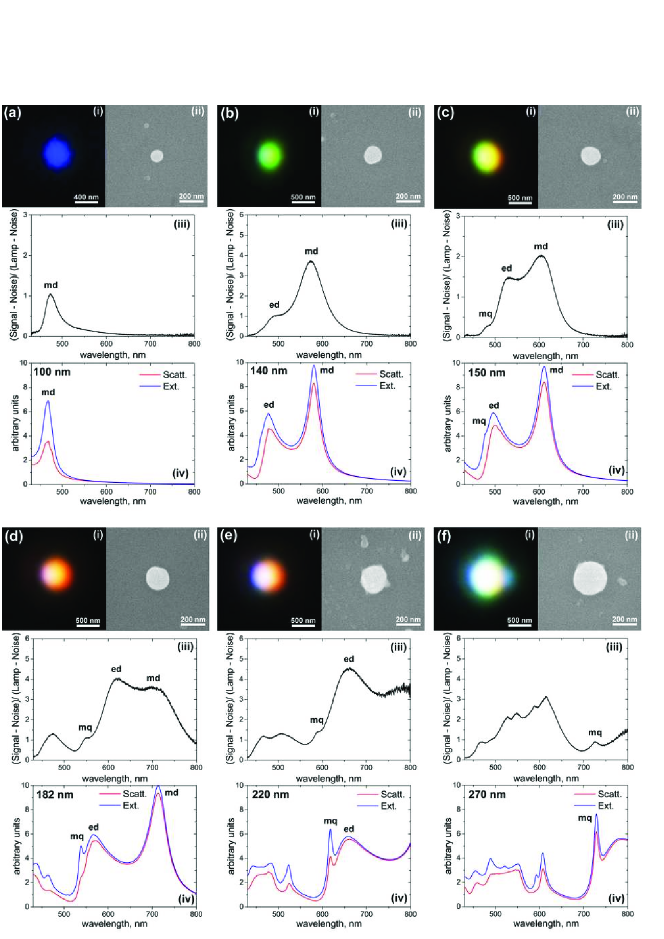
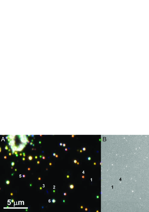
Dark-field microscopic image of a silicon sample ablated by a focused femtosecond laser beam is shown in Fig. 5a. It shines by all the colours of the rainbow from violet to red. To clarify the origin of this strong scattering we selected some nanoobjects shining with different colours on the sample (see Fig. 5a) and measured their scattering spectra by single nanoparticle dark-field spectroscopy. Then, the same sample area was characterized by scanning electron microscopy and the selected nanoobjects providing different colours have been identified (see Fig. 5b, the dark-field microscope image is inverted in horizontal direction relative to that of the SEM). The results of this comparative analysis of the same nanoobjects by dark-field optical microscopy, dark-field scattering spectroscopy, and scanning electron microscopy are presented in Fig. 6. As it can be seen from the SEM images the observed colours are provided by silicon nanoparticles of almost perfect spherical shape and varied sizes. This makes it possible to analyze scattering properties of these nanoparticles in the frames of Mie theory [72] and identify the nature of optical resonances observed in our spectral measurements. The bottom panels (iv) in Fig. 6 represent a total extinction cross-section calculated using Mie theory [72] for silicon nanoparticles of different sizes (the calculations were done in free space). In these calculations, the size of the nanoparticles in each figure was chosen to be similar to the size defined from each corresponding SEM image (ii). It can be seen that there is a clear correlation between the experimental (iii) and theoretical spectra (iv) both in the number and position of the observed resonances. This makes it obvious that Mie theory describes more or less accurately our experimental results.
One of the main advantages of the analytical Mie solution compared to other computational methods is its ability to split the observed spectra into separate contributions of different multipole modes and have a clear picture of the field distribution inside the particle at each resonance maximum. This analysis was done for each particle size in Fig. 6 and corresponding multipole contributions were identified (see notations in the experimental and theoretical spectra). According to this analysis the first strongest resonance of these nanoparticles appearing in the longer wavelength part of the spectrum corresponds to magnetic dipole response (md). Electric field inside the particle at this resonance wavelength has a ring shape while magnetic field oscillates in the particle center. Magnetic dipole resonance is the only peak observed for the smallest nanoparticles (see Fig. 6a). At increased nanoparticle size (see Fig. 6b,c) electric dipole (ed) resonance also appears at the blue part of the spectra, while magnetic dipole shifts to the red. For relatively small nanoparticles, the observed colour is mostly defined by the strongest resonance peak and changes from blue to green, yellow, and red when magnetic resonance wavelength shifts from 480 nm to 700 nm (see Fig. 6a–d). So, we can conclude that the beautiful colours observed in the dark field microscope (see Fig. 5a) correspond to magnetic dipole scattering of the silicon nanoparticles, “magnetic light”. Further increase of the nanoparticle size leads to the shift of magnetic and electric dipole resonances further to the red and infra-red frequencies, while higher multipole modes such as magnetic and electric quadrupoles appear in the blue part of the spectra (see Fig. 6d–f).
Some differences between experimental and theoretical spectra observed in Fig. 6 can be attributed to the presence of silicon substrate, which is not taken into account in our simple Mie theory solution. We should also mention that very similar results have been published almost simultaneously by a different group of authors [73] who demonstrated magnetic and electric dipole resonances of silicon particles in red and near-IR spectral range.
Recently we have also experimentally demonstrated for the first time directional light scattering by spherical silicon nanoparticles in the visible spectral range [74]. These unique scattering properties arise due to simultaneous excitation and mutual interference of magnetic and electric dipole resonances inside a single nanosphere. This phenomenon is similar to a known since long time Kerker-type scattering predicted in [75] for hypothetical magneto-dielectric nanoparticles but never observed experimentally. Directivity of the far-field radiation pattern can be controlled by changing light wavelength and the nanoparticle size. Forward-to-backward scattering ratio above 6 was experimentally obtained at visible wavelengths. Similar directional light scattering by spherical ceramic particles in GHz [76] and GaAs nanodisks in the visible [77] has also been published almost simultaneously by different groups of authors. These unique optical properties of high-refractive index dielectric nanostructures constitute the background for our approach to all-dielectric nanoantennas, which will be discussed in detail below.
2 Huygens optical elements and Yagi—Uda nanoantennas based on dielectric nanoparticles
Recently, it was suggested [8, 45, 46, 40, 41, 42, 9] a novel type of optical nanoantennas made of all-dielectric elements. Moreover, we argue that, since the source of electromagnetic radiation is applied externally, dielectric nanoantennas can be considered as the best alternative to their metallic counterparts. First, dielectric materials exhibit low loss at the optical frequencies. Second, as was suggested earlier, nanoparticles made of high-permittivity dielectrics may support both electric and magnetic resonant modes. This feature may greatly expand the applicability of optical nanoantennas for, e.g. for detection of magnetic dipole transitions of molecules [78]. In our study we concentrate on nanoparticles made of silicon. The real part of the permittivity of the silicon in the visible spectral range is about [79], while the imaginary part is up to two orders of magnitude smaller than that of nobel metals (silver and gold).
1 General concept
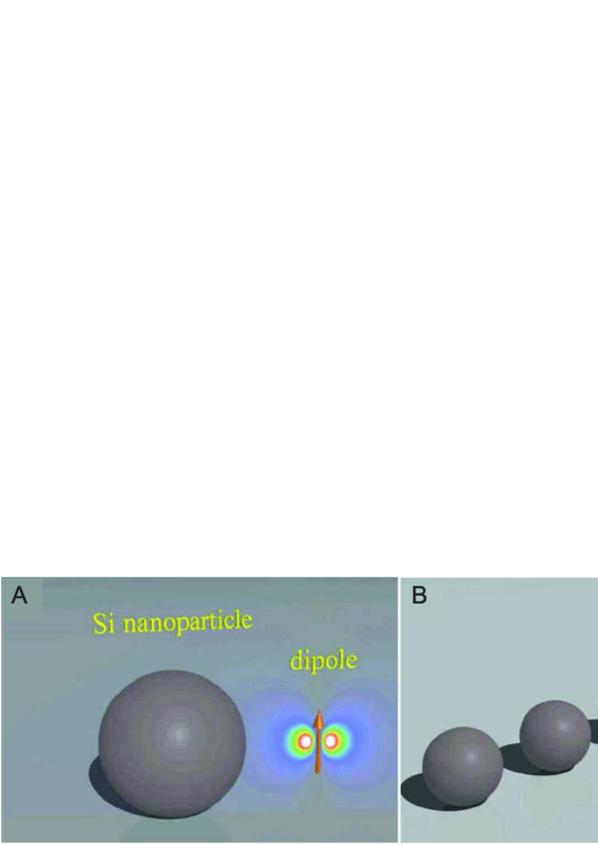
The mentioned above properties of dielectric nanoparticles allow us to realize optical Huygens source [80] consisting of a point-like electric dipole operating at the magnetic resonance of a dielectric nanosphere (see Fig.7A). Such a structure exhibits high directivity with vanishing backward scattering and polarization independence, being attractive for efficient and compact designs of optical nanoantennas.
We start our analysis by considering a radiation pattern of two ideal coupled electric and magnetic dipoles. A single point-like dipole source generates the electric far-field of the following form
| (1) |
where is the electric dipole, is the wavenumber, is the scattered direction, and is the distance from the dipole source. The radiation pattern in the plane of the dipole is proportional to the standard figure-eight profile, , where is the scattered angle. In the plane orthogonal to the dipole () the radiation pattern remains constant and angle independent, . Thus, the total radiation pattern of a single dipole emitter is a torus which radiates equally in the opposite directions. If we now place, in addition to the electric dipole, an orthogonal magnetic dipole located at the same point, the situation changes dramatically. The magnetic dipole generates the electric far-field of the form
| (2) |
Thus, the total electric field is a sum of two contributions from both electric and magnetic dipoles . By assuming that the magnetic dipole is related to the electric dipole via the relation , which corresponds to an infinitesimally small wavefront of a plane wave often called a Huygens source [80], the radiation pattern becomes . This radiation pattern is quite different compared to that of a single electric dipole. It is highly asymmetric with the total suppression of the radiation in a particular direction, [], and a strong enhancement in the opposite direction, . The complete three-dimensional radiation pattern resembles a cardioid or apple-like shape, which is also azimuthally independent. Such a radiation pattern of the Huygens source is potentially very useful for various nanoantenna applications. However, while electric dipole sources are widely used in optics, magnetic dipoles are less common.
First, we consider an electric dipole source placed in a close proximity to a dielectric sphere [see Fig. 7(a)]. As was mentioned above, it can be analytically shown that high permittivity dielectric nanoparticles exhibit strong magnetic resonance in the visible range when the wavelength inside the nanoparticle equals its diameter [81], where and are refractive index and radius of the nanoparticle, respectively. There are many dielectric materials with high enough real part of the permittivity and very low imaginary part, indicating low dissipative losses. To name just a few, silicon (Si, ), germanium (Ge, ), aluminum antimonide (AlSb, ), aluminum arsenide (AlAs, ), and other. In our study we concentrate on the nanoparticles made of silicon, which support strong magnetic resonance in the visible range for the radius varying from nm to nm [69].
For such a small radius compared to the wavelength , the radiation pattern of the silicon nanoparticle in the far field at the magnetic or electric resonances will resemble that of magnetic or electric point-like dipole, respectively. Moreover, it is even possible to introduce magnetic and electric polarisabilities [69, 72, 82] based on the Mie dipole scattering coefficients and :
| (3) |
Thus, the dielectric nanoparticle excited by the electric dipole source at the magnetic resonance may result in the total far field radiation pattern which is similar to that of the Huygens source. Similar radiation patterns can be achieve in light scattering by a magnetic particle when permeability equals permittivity , also known as Kerker’s condition [75]. Our result suggests that even a dielectric nonmagnetic nanoparticle can support two induced dipoles of equal strength resulting in suppression of the radiation in the backward direction. Thus, it can be considered as the simplest and efficient optical nanoantenna with very good directivity.
In general, both polarisabilities and are nonzero in the optical region [69]. It is known that for a dipole radiation in the far field the electric and magnetic components should oscillate in phase to have nonzero energy flow. In the near field the electric and magnetic components oscillate with phase difference, thus, the averaged Poynting vector vanishes, and a part of energy is stored in the vicinity of the source. In the intermediate region, the phase between two components varies form to 0. Placing a nanoparticle close to the dipole source will change the phase difference between two components, and, thus, will affect the amount of radiation form the near field. In the case of plasmonic nanoparticles which exhibit electric polarizability only, there is an abrupt phase change from 0 to in the vicinity of the localized surface plasmon resonance, which makes it difficult to tune plasmonic nanoantennas for optimal performance. The dependence of the scattering diagram on the distance between the electric dipole source and metallic nanoparticle was studied in Ref. [83]. On contrary, in the case of nanoparticles with both electric and magnetic polarisabilities, it is possible to achieve more efficient radiation from the near to far field zone, due to subtle phase manipulation. This is exactly the case of the dielectric nanoparticles.
Any antenna is characterized by two specific properties, directivity and radiation efficiency , defined as [84, 80]
| (4) |
where and are integrated radiated and absorbed powers, respectively, and are spherical angles of standard spherical coordinate system, and is the radiated power in the given direction and/or .
The directivity measures the power density of the antenna radiated in the direction of its strongest emission, while Radiation Efficiency measures the electrical losses that occur throughout the antenna at a given wavelength. To calculate these quantities numerically for the structures shown in Fig. 7a, we employ CST Microwave Studio. To get reliable results, we model the electric dipole source by a Discrete Port coupled to two PEC nanoparticles.
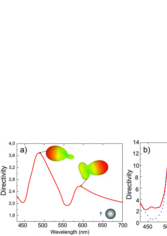
In Fig. 8(a) we show the dependence of the directivity on wavelength for a single dielectric nanoparticle excited by a electric dipole source. Two inserts demonstrate 3D angular distribution of the radiated pattern corresponding to the local maxima. In this case, the system radiates predominantly to the forward direction at nm, while in another case, the radiation is predominantly in the backward direction at nm. In this case, the total electric dipole moment of the sphere and point-like source and the magnetic dipole moment of the sphere oscillate with the phase difference , resulting in the destructive interference in the forward direction. At the wavelength nm the total electric and magnetic dipole moments oscillate in phase and produce Huygens-source-like radiation pattern with the main lobe directed in the forward direction.
By adding more elements to the silicon nanoparticle, we can enhance the performance of all-dielectric nanoantennas. In particular, we consider a dielectric analogue of the Yagi-Uda design (see Fig.7) consisting of four directors and one reflector. The radii of the directors and the reflector are chosen to achieve the maximal constructive interference in the forward direction along the array. The optimal performance of the Yagi-Uda nanoantenna should be expected when the radii of the directors correspond to the magnetic resonance, and the radius of the reflector correspond to the electric resonance at a given frequency, with the coupling between the elements taken into account. Our particular design consists of the directors with radii nm and the reflector with the radius nm. In Fig. 8(b) we plot the directivity of all-dielectric Yagi-Uda nanoantenna vs. wavelength with the separation distance nm. Inserts demonstrate the 3D radiation patterns at particular wavelengths. We achieve a strong maximum at nm. The main lobe is extremely narrow with the beam-width about and negligible backscattering. The maximum does not correspond exactly to either magnetic or electric resonances of a single dielectric sphere, which implies the importance of the interaction between constitutive nanoparticles.
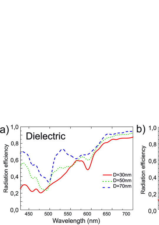
As the next step, we study the performance of the all-dielectric nanoantennas for different separation distances , and compare it with a plasmonic analogue of the similar geometric design made of silver nanoparticles. According to the results summarized in Fig. 9, the radiation efficiencies of both types of nanoantennas are nearly the same for larger separation of directors nm with the averaged value . Although dissipation losses of silicon are much smaller than those of silver, the dielectric particle absorbs the EM energy by the whole spherical volume, while the metallic particles absorb mostly at the surface. As a result, there is no big difference in the overall performance of these two types of nanoantennas for relatively large distances between the elements. However, the difference becomes very strong for smaller separations. The radiation efficiency of the all-dielectric nanoantenna is insensitive to the separation distance [see Fig. 9 (a)]. On contrary, the radiation efficiency drops significantly for metallic nanoantennas [see Fig. 9 (b)].
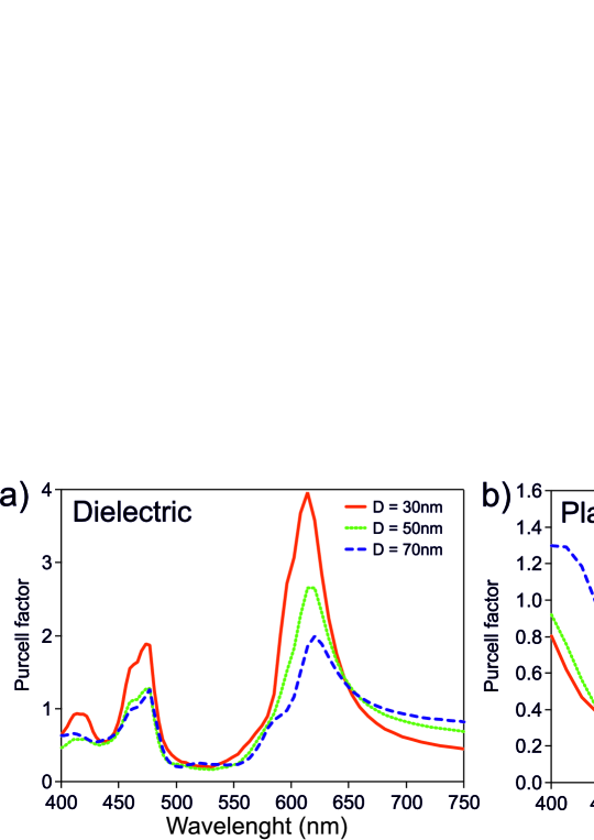
Finally, we investigate the modification of the transition rate of a quantum point-like source placed in the vicinity of dielectric particles. For electric-dipole transitions and in the weak-coupling regime, the normalised spontaneous decay rate , also known as Purcell factor, can be calculated classically as the ratio of energy dissipation rates of an electric dipole [7]. Here, and correspond to transition rate of the quantum emitter and energy dissipation rate of the electric dipole in free space [85]. In the limit of the intrinsic quantum yield of the emitter close to unity, both ratios become equal to each other , which allows us to calculate the Purcell factor in the classical regime [7]. We have calculated the Purcell factor by using both, numerical and analytical approaches. Numerically, by using the CST Microwave Studio we calculate the total radiated in the far-field and dissipated into the particles powers and take the ratio of their sum to the total power radiated by the electric dipole in free space. Analytically, we employed the generalised multiparticle Mie solution [86] adapted for the electric dipole excitation [87]. We verified that both approaches produce similar results. In Fig. 10 we show calculated Purcell factor of the all-dielectric Yagi-Uda nanoantenna vs. wavelength for various separation distances. We observe that, by decreasing the separation between the directors, the Purcell factor becomes stronger near the magnetic dipole resonance. We can notice that a plasmonic analogue of the same nanoantenna made of Ag exhibits low Purcell factor less than one. Thus, such relatively high Purcell factor can be employed for efficient photon extraction from molecules placed near all-dielectric optical nanoantennas.
2 Experimental verification of dielectric Yagi-Uda nanoantenna
There are exist some technological issues to reproduce an object of the nanometer size with a high accuracy. For this reason we have scaled the dimensions of the proposed optical all-dielectric Yagi-Uda nanoantenna to the microwave frequency range while keeping all the material parameters in order to study the microwave analogue of the nanoantenna experimentally. We use the design of the Yagi-Uda antenna shown in Fig. 7b. To mimic the silicon spheres in microwave frequency range, we employ MgO-TiO2 ceramic which is characterized by dielectric constant of 16 and dielectric loss factor of (1.121.17)10-4 measured at frequency 9-12 GHz [88]. As a source, we use a half-wavelength vibrator. We study experimentally both the radiation pattern and directivity of the antenna.
We set the radius of the reflector equal to mm. The frequencies of the electric and magnetic Mie resonances of the sphere calculated with the help of Eq. (3) are 10.2 GHz and 7 GHz, respectively. The radius of the directors is mm. In this case, the frequencies of the electric and magnetic Mie resonances are 12.5 GHz and 9 GHz. As a source, we model a half-wavelength vibrator with the total length of mm and diameter of mm. The distances between the reflector, directors, and vibrator have been adjusted by numerical simulations. We achieve an effective suppression of the back and minor lobes, and the narrow major lobe (of about 40∘) of the antenna when the distance between the director’s surface as well as the distance between vibrator center and the first director surface are 1.5 mm; the distance between the surface of the reflector and vibrator centre is 1.1 mm.
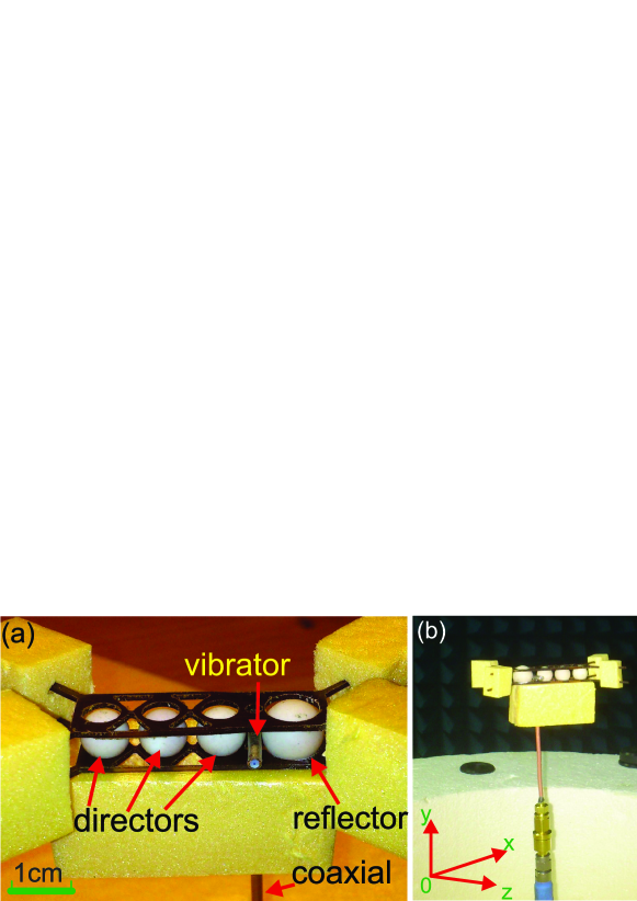
Figures 11(a,b) show the photographs of the fabricated all-dielectric Yagi-Uda antenna. The reflector and directors are made of MgO-TiO2 ceramic with accuracy of 0.05 mm. To fasten together the elements of the antenna and vibrator, we use a special holder made of a thin dielectric substrate with dielectric permittivity close to 1 [being shown in Fig. 11(a)]. Styrofoam material with the dielectric permittivity of 1 is used to fix the antenna in the azimuthal-rotation unit [see Fig. 11(b)]. To feed the vibrator, we employ a coaxial cable that is connected to an Agilent PNA E8362C vector network analyzer.
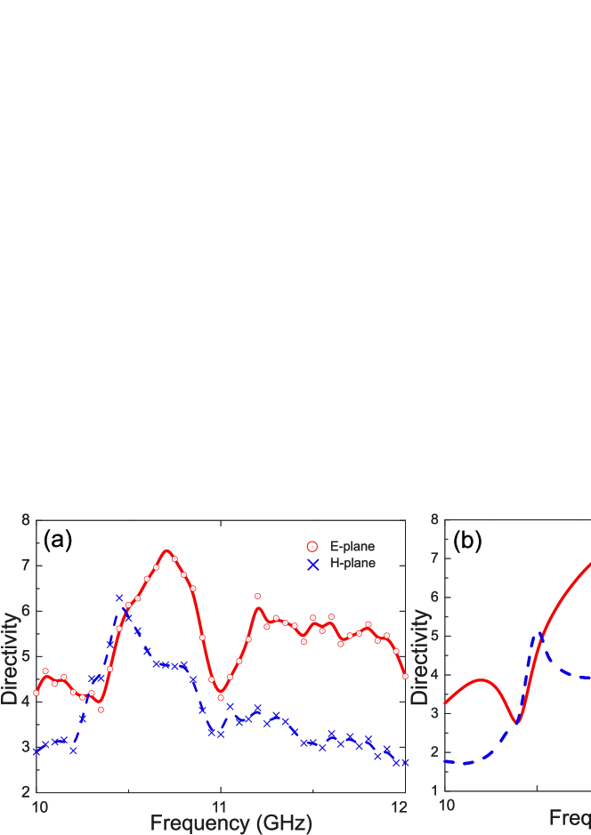
Any antenna is characterized by the total directivity (4). Sometimes it is not possible to determine the value of the total directivity experimentally due to difficulties to measure the total radiated power . In this case, it is convenient to use directivity in the planes where electric field and magnetic field oscillate in the far field. For our coordinates the directivity in the evaluation plane (E-plane) and the azimuthal plane (H-plane) can be expressed as:
| (5) |
Equations (5) are multiplied by because of the integration in the denominator is performed only for one coordinate while the second coordinate is fixed.
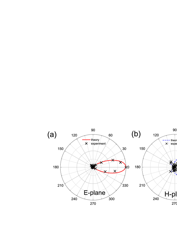
To extract the antenna directivity in the - and -planes from the experimental data, we measure the radiated power by the antenna in the frequency range from 10 GHz to 12 GHz with a step of 50 MHz. Then, by employing Eq. (5) we calculate the directivity at each frequency. The results are presented in Fig. 12a. To estimate the performance of the all-dielectric Yagi-Uda antenna at microwaves, we simulate numerically the antenna’s response by employing the CST Microwave Studio. We observe excellent agreement between numerical results of Fig. 12b and measured experimental data. However, we notice a small frequency shift of the measured directivity (approx. ) in comparison with the numerical results. This discrepancies can be explained by the effect of the antenna holders in the experiment, not included into the numerical simulation.
The antenna radiation patterns in the far field (at the distance m) are measured in an anechoic chamber by a horn antenna and rotating table. The measured radiation patterns of the antenna in - and -planes at the frequency 10.7 GHz are shown in Fig. 13. The measured characteristics agree very well with the numerical results. A small disagreement can be explained by the presence of the antenna holder which influence was not taken into account in our numerical simulations.
3 All–dielectric superdirective optical nanoantenna
For optical wireless circuits on a chip, nanoantennas are required to be both highly directive and compact [12, 89, 90, 91]. In nanophotonics, directivity has been achieved for arrayed plasmonic antennas utilizing the Yagi-Uda design [84, 92, 90, 37, 93], large dielectric spheres [94], and metascreen antennas [95]. Though individual elements of these arrays are optically small, the overall size of the radiating systems is larger than the radiation wavelength . In addition, small plasmonic nanoantennas possess weak directivity close to the directivity of a point dipole [90, 96, 97].
As was discussed above, it was suggested theoretically and experimentally to employ magnetic resonances of high-index dielectric nanoparticles for enhancing the nanoantenna directivity [8, 45, 46, 40, 41, 42, 9, 37, 98]. High-permittivity nanoparticles can have nearly resonant balanced electric and magnetic dipole responses. This balance of the electric and magnetic dipoles oscillating with the same phase allows the practical realization of the Huygens source, an elementary emitting system with a cardioid pattern [80, 44, 46, 37] and with the directivity larger than 3.5. Importantly, a possibility to excite magnetic resonances leads to the improved nanoantenna directional properties without a significant increase of its size.
Superdirectivity has been already discussed for radio-frequency antennas, and it is defined as directivity of an electrically small radiating system that significantly exceeds (at least in 3 times) directivity of an electric dipole [80, 99, 100]. In that sense, the Huygens source is not superdirective. In the antenna literature, superdirectivity is claimed to be achievable only in antenna arrays by the price of ultimately narrow frequency range and by employing very precise phase shifters (see, e.g., Ref. [80, 99, 100]). Therefore, superdirective antennas, though very desirable for many applications such as space communications and radioastronomy, were never demonstrated and implemented for practical applications.
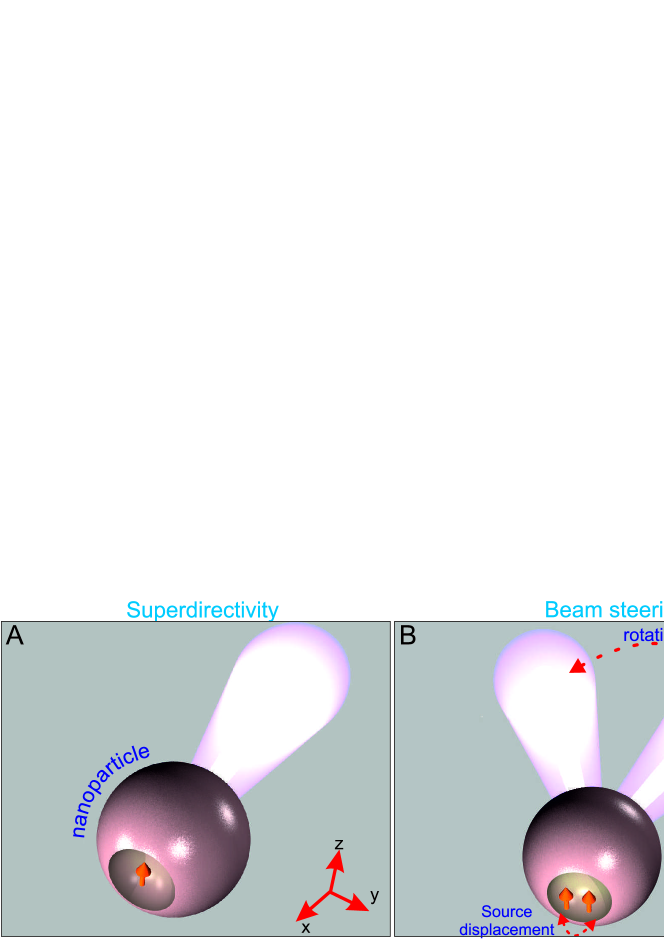
Superdirectivity was predicted theoretically for an antenna system [95] where some phase shifts were required between radiating elements to achieve complex shapes of the elements of a radiating system which operates as an antenna array. In this paper, we employ the properties of subwavelength particles excited by an inhomogeneous field with higher-order magnetic multipoles. We consider a subwavelength dielectric nanoantenna (with the size of 0.4 wavelength) with a notch resonator excited by a point-like emitter located in the notch. The notch transforms the energy of the generated magneto-dipole Mie resonance into high-order multipole moments, where the magnetic multipoles dominate. This system is resonantly scattering i.e. it is very different from dielectric lenses and usual dielectric cavities which are large compared to the wavelength. Another important feature of the notched resonator is its huge sensitivity of the radiation direction to a spatial position of the emitter. This property leads to a strong beam steering effect and subwavelength sensitivity of the radiation direction to the source location. The proposed design of superdirective nanoantennas may also be useful for collecting single-source radiation, monitoring quantum objects states, and nanoscale microscopy.
In order to achieve superdirectivity, we should generate subwavelength spatial oscillations of the radiating currents [80, 99, 100]. Then, near fields of the antenna become strongly inhomogeneous, and the near-field zone expands farther than that of a point dipole. The effective antenna aperture can be defined as , where the maximum of directivity , is the wavelength in free space in our case, and are respectively the maximum power in the direction of the radiation pattern and the total radiation power. By normalizing the effective aperture S by the geometric aperture for a spherical antenna , we obtain the definition of superdirectivity [99, 80]:
| (6) |
Practically, the value is sufficient for superdirectivity of a sphere. In this work, maximum of 6.5 for is predicted theoretically for the optical frequency range, and the value of 5.9 is demonstrated experimentally for the microwave frequency range.
1 Concept of all–dielectric superdirective optical nanoantennas
Here we demonstrate a possibility to create a superdirective nanoantenna without hypothetic metamaterials and plasmonic arrays. We consider a silicon nanoparticle, taking into account the frequency dispersion of the dielectric permittivity [79]. The radius of the silicon sphere is equal in our example to nm. For a simple sphere under rather homogeneous (e.g. plane-wave) excitation, only electric and magnetic dipoles can be resonantly excited while the contribution of higher-order multipoles is negligible in the visible [37]. Making a notch in the sphere breaks the symmetry and increases the contribution of higher-order multipoles into scattering even if the sphere is still excited homogeneously. Further, placing a nanoemitter (e.g. a quantum dot) inside the notch, as shown in Fig. 14 we create the conditions for the resonant excitation of multipoles: the field exciting the resonator is now spatially very non-uniform as well as the field of a set of multipoles. In principle, the notched particle operating as a nanoantenna can be performed by different semiconductor materials and have various shapes – spherical, ellipsoidal, cubic, conical, as well as the notch. However, in this work, the particle is a silicon sphere and the notch has the shape of a hemisphere with a radius . The emitter is modeled as a point-like dipole and it is shown in Fig. 14 by a red arrow.
It is important to mention that our approach is seemingly close to the idea of references [101, 102] where a small notch on a surface of a semiconductor microlaser was used to achieve higher emission directivity by modifying the field distribution inside the resonator [103]. An important difference between those earlier studies and our work is that the design discussed earlier is not optically small and the directive emission is not related to superdirectivity. In our case, the nanoparticle is much smaller than the wavelength, and our design allows superdirectivity. For the same reason our nanoantenna is not dielectric [104, 105] or Luneburg [106, 107] lenses. For example, immersion lenses [108, 109, 110, 111] are the smallest from known dielectric lenses, characterized by the large size 1-2 m in optical frequency range. The working methodology of such lenses is to collect a radiation by large geometric aperture S, while . Our approach demonstrates that the subwavelength system, with small geometric aperture, can have high directing power because of an increase of the effective aperture. Moreover, there are articles (see. references [85, 112]) where the transition rates of atoms inside and outside big dielectric spheres with low dielectric constant (approximately 2), were studied.
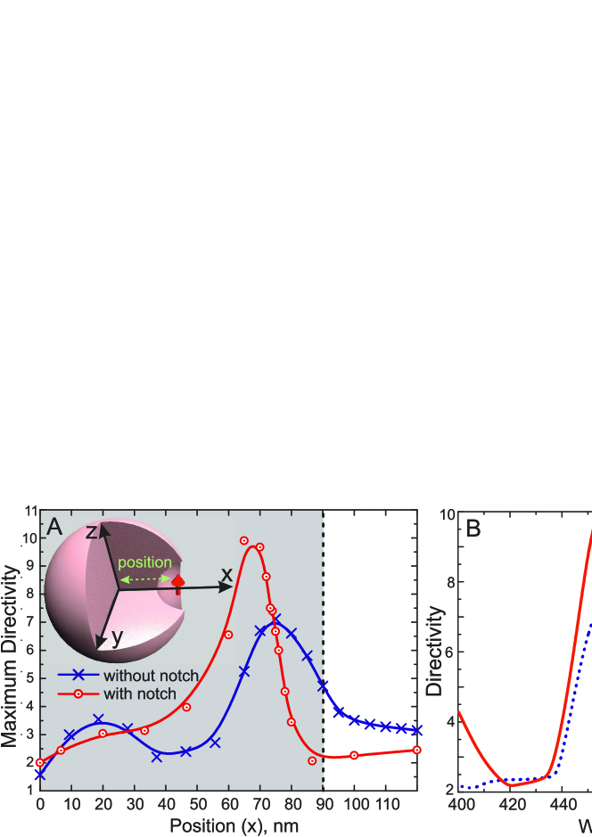
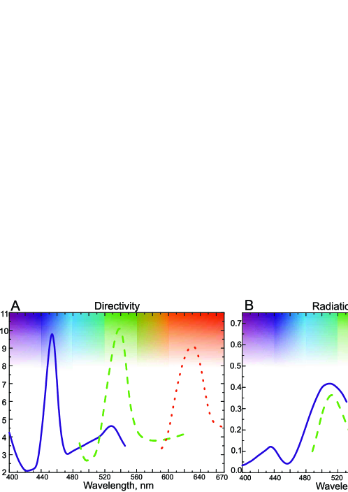
First, we consider a particle without a notch but excited inhomogeneously by an emitter point. To study the problem numerically, we employed the simulation software CST Microwave Studio. Image Fig. 15A shows the dependence of the maximum directivity on the position of the source in the case of a sphere nm without a notch, at the wavelength nm (blue curve with crosses). This dependence has the maximum () when the emitter is placed inside the particle at the distance 20 nm from its surface. The analysis shows that in this case the electric field distribution inside a particle corresponds to the noticeable excitation of higher-order multipole modes not achievable with the homogeneous excitation.
Furthermore, the amplitudes of high-order multipoles are significantly enhanced with a small notch around the emitter, as it is shown in Fig. 14. This geometry transforms it into a resonator with high-order multipole moments. In this example the center of the notch is on the nanosphere’s surface. The optimal radius of the notch (for maximal directivity) is nm. In Fig. 15A the extrapolation red curve with circles, corresponding to simulation results, shows the maximal directivity versus the location of the emitter at the wavelength 455 nm. The Fig. 15B shows the directivity versus with and without a notch, it exhibits a maximum of 10 for the directivity at 455 nm. The inset shows the three-dimensional radiation pattern of the structure at 455 nm. This pattern has an angular width (at the level of 3 dB) of the main lobe equal to . This value of directivity corresponds to the normalized effective aperture .
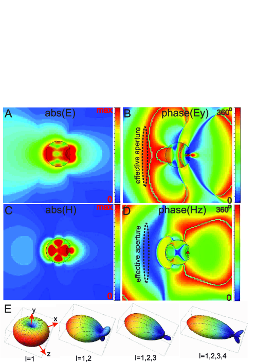
Figures Fig. 16A and B show the distribution of the absolute values and phases of the internal electric field in the vicinity of the nanoantenna. Electric and magnetic fields inside the particle are strongly inhomogeneous at 455 nm i.e. in the regime of the maximal directivity. In this regime, the internal area where the electric field oscillates with approximately the same phase turns out to be maximal. This area is located near the back side of the spherical particle, as can be seen in figure Fig. 16B,D. In other words, the effective near zone of the nanoantenna is maximal in the superdirective regime.
Usually, high directivity of plasmonic nanoantennas is achieved by the excitation of higher electrical multipole moments in plasmonic nanoparticles [83, 113, 114] or for core-shell resonators consisting of a plasmonic material and a hypothetic metamaterial which would demonstrate the extreme material properties in the nanoscale [115]. Although, the values of directivity achieved for such nanoantennas do not allow superdirectivity, these studies stress the importance of higher multipoles for the antenna directivity.
Next, we demonstrate how to find multipole modes excited in the all-dielectric superdirective nanoantenna which are responsible for its enhanced directivity. We expand the exactly simulated internal field, producing the polarization currents in the nanoparticle, into multipole moments following to [116]. The expansion is a series of vector spherical harmonics with the coefficients and , which characterize the electrical and magnetic multipole moments [116]:
| (7) |
where and are densities of the total electrical charges and currents that can be easily expressed through the internal electric E and magnetic H fields of the sphere, are the spherical harmonics of the orders and , , are the -order spherical Bessel function and is the speed of light. Coefficients and determine the electric and magnetic mutipole moments, namely dipole at , quadrupole at , octupole at etc.
The multipole coefficients determine not only the mode structure of the internal field but also the angular distribution of the radiation. In particular, in the far field zone electric and magnetic fields of -order multipole depend on the distance as [116] and expression for the angular distribution of the radiation power can be written as follows:
| (8) |
where , is the solid angle element in spherical coordinates and - unit vector of the observation point. All coefficients and give the same contribution to the radiation, if they have the same values. Since higher-order multipoles for optically small systems have usually negligibly small amplitudes compared to and , they are, as a rule, not considered.
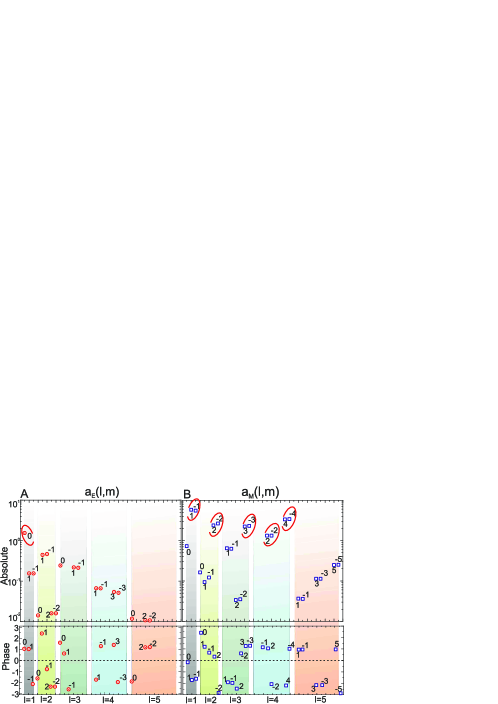
The amplitudes of multipole moments, are found by using the expressions (7) for electric and magnetic fields distribution Fig. 16A-D are shown in Fig. 17, where we observe strong excitation of , , , , , , , , , and . These multipole moments determine the angular pattern of the antenna. All other ones give a negligible contribution. Absolute values of all magnetic moments are larger than those of the electric moments in the corresponding multipole orders, and the effective spectrum of magnetic multipoles is also broader than the one of the electric moments. Thus, the operation of the antenna is mainly determined by the magnetic multipole response. Absolute values of multipole coefficients of the same order are practically equivalent. However, the phase of some coefficients are different. Therefore, the modes with and form a strong anisotropy of the forward–backward directions that results in the unidirectional radiation.
We have performed the transformation of multipole coefficients into an angular distribution of radiation in accordance to (8) by using distribution of the electric and magnetic fields Fig. 16A-D and determined the relative contribution of each order . Fig. 16E shows how the directivity grows versus the spectrum of multipoles with equivalent amplitudes. The right panel of Fig. 16E nearly corresponds to the inset in Fig. 15 that fits to the results shown in Fig. 16E.
Generally, the superdirectivity effect is accompanied by a significant increase of the effective near field zone of the antenna compared to the one of a point dipole for which the near zone radius is equal to . In the optical frequency range this effect is especially important, considering the crucial role of the near fields at the nanoscale.
Usually, the superdirectivity regime corresponds to a strong increase of dissipative losses [80]. Radiation efficiency of the nanoantenna is determined by , where is the accepted input power of the nanoantenna. However, the multipole moments excited in our nanoantenna are mainly of magnetic type that leads to a strong increase of the near magnetic field that dominates over the electric one. Since the dielectric material does not dissipate the magnetic energy, the effect of superdirectivity does not lead to a so large increase of losses in our nanoantenna as it would be in the case of dominating electric multipoles. However, since the electric near field is nonzero the losses are not negligible. At wavelengths 440-460 nm (blue light) the directivity achieves 10 but the radiation efficiency is less than 0.1 (see [Fig. 18)]. This is because silicon has very high losses in this range [79]. Peak of directivity is shifted to longer wavelengths with the increase of the nanoantenna size. For the design parameters corresponding to the operation wavelength 630 nm (red light) the calculated value of radiation efficiency is as high as 0.5, with nearly same directivity close to 10. In the infrared range, there are high dielectric permittivity materials with even lower losses. In principle, the proposed superdirectivity effect is not achieved by price of increased losses, and this is an important advantage compared to known superdirective radio-frequency antenna arrays [80] and compared to their possible optical analogues – arrays of plasmonic nanoantennas.
2 Steering of light at the nanoscale
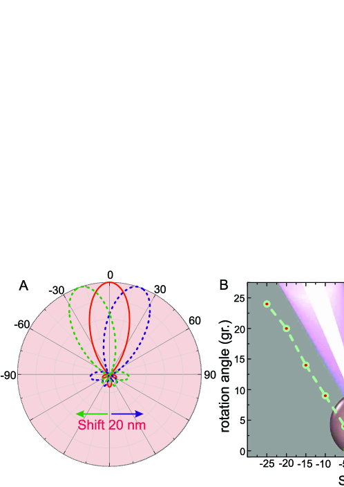
Here we examine the response of the nanoantenna to subwavelength displacements of the emitter. Displacement in the plane perpendicular to the axial symmetry of antenna (i.e. along the axis) leads to the rotation of the beam without damaging the superdirectivity. Fig.19A shows the radiation patterns of the antenna with the source in center (solid line) and the rotation of the beam for the 20 nm left/right offset (dashed lines). Shifting of the source in the right side leads to the rotation of pattern to the left, and vice versa. The angle of the beam rotation is equal to 20 degrees, that is essential and available to experimental observations. The result depends on the geometry of the notch. For a hemispherical notch, the dependence of the rotation angle on the displacement is presented in Fig.19B.
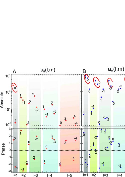
To interpret the beam steering effect, we can consider the result of field expansion to electric and magnetic multipoles, as shown in Fig.20. In the case of asymmetrical location (the 20 nm left offset) of the source in the notch absolute values of are different. This means that the mode is excited more strongly than , or vice versa, that depends on direction of displacement. The effect of superdirectivity remains even with an offset of the source until to the edge of the notch. Small displacements of the source along and do not lead to the rotation of the pattern.
Instead of the movement of a single quantum dot one we can have the emission of two or more quantum dots located near the edges of the notch. In this case, the dynamics of their spontaneous decay will be well displayed in the angular distribution of the radiation. This can be useful for quantum information processing and for biomedical applications.
Beam steering effect described above is similar to the effect of beam rotation in hyperlens [117, 118, 119], where the displacement of a point-like source leads to a change of the angular distribution of the radiation power. However, in our case, the nanoantenna has subwavelength dimensions and therefore it can be neither classified as a hyperlens nor as a micro-spherical dielectric nanoscope [104, 105], moreover it is not an analogue of solid immersion micro-lenses [108, 109, 110, 111], which are characterized by the size 1-5 in the same frequency range. These lens has a subwavelength resolving power due to the large geometric aperture but the value of normalized effective aperture is . Our study demonstrates that the sub-wavelength system, with small compared to the wavelength geometric aperture can have both high directing and resolving power because of a strong increase of the effective aperture compared to the geometrical one.
3 Experimental verification of superdirective optical nanoantenna
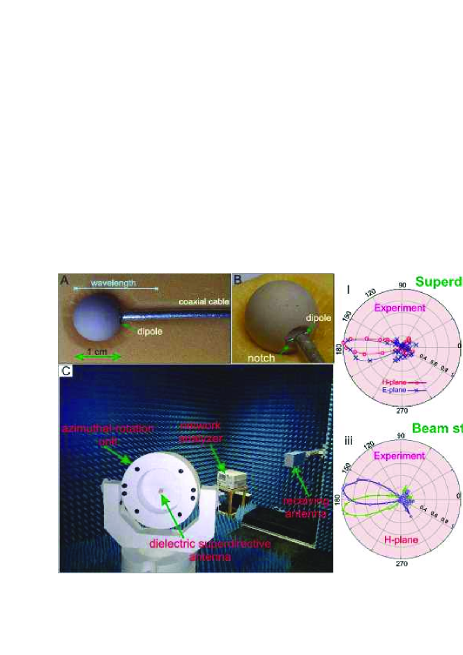
We have confirmed both predicted effects studying the similar problem for the microwave range. Therefore, we have scaled up the nanoantenna as above to low frequencies. Instead of Si we employ MgO-TiO2 ceramic [46] characterized at microwaves by a dispersion-less dielectric constant 16 and dielectric loss factor of 1.1210-4. We have used the sphere of radius mm and applied a small wire dipole [80] excited by a coaxial cable as shown in Fig. 21A,B. The size of the hemispherical notch is approximately equal to mm. Antenna properties have been studied in an anechoic chamber Fig. 21C.
The results of the experimental investigations and numerical simulations of the pattern in both - and -planes are summarized in Figs. 21i,ii. Radiation patterns in both planes are narrow beams with a lobe angle about 35∘. Experimentally obtained coefficients of the directivity in both - and -planes are equal to 5.9 and 8.4, respectively (theoretical predictions for them were respectively equal 6.8 and 8.1). Our experimental data are in a good agreement with the numerical results except a small difference for the E plane, that can be explained by the imperfect symmetry of the emitter. Note, that the observed directivity is close to that of an all-dielectric Yagi-Uda antenna with maximum size of [46]. The maximum size of our experimental antenna is closed to . Thus, our experiment clearly demonstrates the superdirective effect.
Experimental and numerical demonstration of the beam steering effect are presented in Figs. 21iii,iv. For the chosen geometry of antenna, displacement of source by 0.5 mm leads to a beam rotation of about 10∘. Note that the ratio of mm to value of the source displacement 0.5 mm is equal to 37. Therefore the beam steering effect observed at subwavelength source displacement.
Finally, we consider the question of dielectric superdirective antenna matching with coaxial cable. Despite that length of the wire dipole is close to , dielectric superdirective antenna is well matched with the coaxial cable in the operating frequency range. The antenna matching is explained by the strong coupling of the wire dipole with the excited modes of notched dielectric particle and is not related to the dissipative losses in the superdirectivity regime. For this reason, we have not used additional matching devices (e.g. "balun").
Though the concept of the superdirectivity of high-refractive index dielectric particles with notch has now only been proven in GHz spectral range there is a hope that it can be transferred into the visible and near-IR spectrum in the nearest future. Recently we have experimentally demonstrated that it is possible to engineer resonant modes of spherical nanoresonators using a combined approach of laser-induced transfer to generate almost perfect spherical nanoparticles and helium ion beam milling to structure their surface with sub-5nm resolution [120]. This novel approach can become a suitable candidate for realizing all-dielectric superdirective nanoantennas.
Conclusion
We propose a new type of highly efficient Yagi-Uda nanoantenna and introduced a novel concept of superdirective nanoantennas based on silicon nanoparticles. In addition to the electric response, this silicon nanoantennas exhibit very strong magnetic resonances at the nanoscale. Both types of nanoantennas are studied analytically, numerically and experimentally. For superdirective nanoantennas we also predict the effect of the beam steering at the nanoscale characterized by a subwavelength sensitivity of the beam radiation direction to the source position.
The unique optical properties and low losses make dielectric nanoparticles perfect candidates for a design of high-performance nanoantennas, low-loss metamaterials, and other novel all-dielectric nanophotonic devices. The key to such novel functionalities of high-index dielectric nanophotonic elements is the ability of subwavelength dielectric nanoparticles to support simultaneously both electric and magnetic resonances, which can be controlled independently for particles of non spherical forms.
Список литературы
- [1] P. Bharadwaj, B. Deutsch, and L. Novotny, ‘‘Optical antennas,’’ Advances in Optics and Photonics 1, pp. 438–483, 2009.
- [2] L. Novotny and N. van Hulst, ‘‘Antennas for light,’’ Nat. Photon. 5, pp. 83–90, 2011.
- [3] A. G. Curto, G. Volpe, T. H. Taminiau, M. P. Kreuzer, R. Quidant, and N. F. van Hulst, ‘‘Unidirectional emission of a quantum dot coupled to a nanoantenna,’’ Science 329, pp. 930–933, 2010.
- [4] T. Taminiau, F. Stefani, F. Segerink, and N. V. Hulst, ‘‘Optical antennas direct single-molecule emission,’’ Nat. Photonics. 2, pp. 234–237, 2008.
- [5] L. Novotny, ‘‘Optical antennas tuned to pitch,’’ Nature 455, p. 887, 2008.
- [6] S. He, Y. Cui, Y. Ye, P. Zhang, and Y. Jin, ‘‘Optical nanoantennas and metamaterials,’’ Materials Today 12, p. 16, 2009.
- [7] L. Novotny and B. Hecht, Principles of Nano-Optics, Cambridge University Press, 2006.
- [8] A. Krasnok, I. Maksymov, A. Denisyuk, P. Belov, A. Miroshnichenko, C. Simovski, and Y. Kivshar, ‘‘Optical nanoantennas,’’ Phys.-Usp. 56, p. 539, 2013.
- [9] A. Krasnok and P. Belov, Optical nanonatennas, LAP LAMBERT Academic Publishing, 2013.
- [10] M. W. Knight, H. Sobhani, P. Nordlander, and N. J. Halas, ‘‘Photodetection with active optical antennas,’’ Science 332, pp. 702–704, 2011.
- [11] M. F. Garcia-Parajo, ‘‘Optical antennas focus in on biology,’’ Nature Photonics 2, pp. 201–203, 2008.
- [12] A. Alu and N. Engheta, ‘‘Wireless at the nanoscale: Optical interconnects using matched nanoantennas,’’ Phys. Rev. Lett. 104, p. 213902, 2010.
- [13] B. J. Roxworthy, K. D. Ko, A. Kumar, K. H. Fung, E. K. C. Chow, G. L. Liu, N. X. Fang, and K. C. Toussaint, ‘‘Application of plasmonic bowtie nanoantenna arrays for optical trapping, stacking, and sorting,’’ Nano Lett. 12, pp. 796–801, 2012.
- [14] A. Andryieuski, R. Malureanu, G. Biagi, T. Holmgaard, and A. Lavrinenko, ‘‘Compact dipole nanoantenna coupler to plasmonic slot waveguide,’’ Opt. Lett. 37, pp. 1124–1126, 2012.
- [15] B. Khlebtsov, A. Melnikov, V. Zharov, and N. Khlebtsov, ‘‘Absorption and scattering of light by a dimer of metal nanospheres: comparison of dipole and multipole approaches,’’ Nanotechnology 17, p. 1437, 2006.
- [16] F. Gonzalez and G. Boreman, ‘‘Comparison of dipole, bowtie, spiral and log-periodic ir antennas,’’ Infrared Phys. Tech. 46, pp. 418–428, 2005.
- [17] Z. Fang, L. Fan, C. Lin, D. Zhang, A. J. Meixner, and X. Zhu, ‘‘Plasmonic coupling of bow tie antennas with ag nanowire,’’ Nano Lett. 11, 2011.
- [18] H. Guo, T. P. Meyrath, T. Zentgraf, N. Liu, L. Fu, H. Schweizer, and H. Giessen, ‘‘Optical resonances of bowtie slot antennas and their geometry and material dependence,’’ Opt. Express 16, pp. 7756–7766, 2008.
- [19] N. A. Hatab, C.-H. Hsueh, A. L. Gaddis, S. T. Retterer, J.-H. Li, G. Eres, Z. Zhang, and B. Gu, ‘‘Free-standing optical gold bowtie nanoantenna with variable gap size for enhanced raman spectroscopy,’’ Nano Lett. 10, 2010.
- [20] A. Kinkhabwala, Z. Yu, S. Fan, Y. Avlasevich, K. Mullen, and W. E. Moerner, ‘‘Large single-molecule fluorescence enhancements produced by a bowtie nanoantenna,’’ Nat. Phot. 3, pp. 654–657, 2009.
- [21] K. D. Ko, A. Kumar, K. H. Fung, R. Ambekar, G. L. Liu, N. X. Fang, and K. C. Toussaint, ‘‘Nonlinear optical response from arrays of au bowtie nanoantennas,’’ Nano Lett. 11, 2011.
- [22] S. Sederberg and A. Y. Elezzabi, ‘‘Nanoscale plasmonic contour bowtie antenna operating in the mid-infrared,’’ Opt. Express 19, pp. 15532–15537, 2011.
- [23] J. Y. Suh, M. D. Huntington, C. H. Kim, W. Zhou, M. R. Wasielewski, and T. W. Odom, ‘‘Extraordinary nonlinear absorption in 3d bowtie nanoantennas,’’ Nano Lett. 12, 2012.
- [24] Z. Zhang, A. Weber-Bargioni, S. W. Wu, S. Dhuey, S. Cabrini, and P. J. Schuck, ‘‘Manipulating nanoscale light fields with the asymmetric bowtie nano-colorsorter,’’ Nano Lett. 9, pp. 4505–4509, 2009.
- [25] A. Alu and N. Engheta, ‘‘Input impedance, nanocircuit loading, and radiation tuning of optical nanoantennas,’’ PRL 101, p. 043901, 2008.
- [26] A. Alu and N. Engheta, ‘‘Tuning the scattering response of optical nanoantennas with nanocircuit loads,’’ Nat. Phot. 2, pp. 307–310, 2008.
- [27] T. Coenen, E. J. R. Vesseur, A. Polman, and A. F. Koenderink, ‘‘Directional emission from plasmonic yagi-uda antennas probed by angle-resolved cathodoluminescence spectroscopy,’’ Nano Lett. 11, pp. 3779–3784, 2011.
- [28] J. Dorfmuller, D. Dregely, M. Esslinger, W. Khunsin, R. Vogelgesang, K. Kern, and H. Giessen, ‘‘Near-field dynamics of optical yagi-uda nanoantennas,’’ Nano Lett. 11, pp. 2819–2824, 2011.
- [29] H. F. Hofmann, T. Kosako, and Y. Kadoya New Journal of Physics 9, p. 217, 2007.
- [30] G. Lerosey, ‘‘Nano-optics: Yagi–uda antenna shines bright,’’ Nat. Phot. 4, pp. 267–268, 2010.
- [31] J. Li, A. Salandrino, and N. Engheta, ‘‘Optical spectrometer at the nanoscale using optical yagi-uda nanoantennas,’’ Phys. Rev. B 79, p. 195104, 2009.
- [32] S. V. Lobanov, T. Weiss, D. Dregely, H. Giessen, N. A. Gippius, and S. G. Tikhodeev, ‘‘Emission properties of an oscillating point dipole from a gold yagi-uda nanoantenna array,’’ Phys. Rev. B 85, p. 155137, 2012.
- [33] I. S. Maksymov, I. Staude, A. E. Miroshnichenko, and Y. S. Kivshar, ‘‘Optical yagi-uda nanoantennas,’’ Nanophotonics 1, pp. 65–81, 2012.
- [34] I. S. Maksymov, A. E. Miroshnichenko, and Y. S. Kivshar, ‘‘Actively tunable bistable optical yagi-uda nanoantenna,’’ Opics Express 20, pp. 8929–8938, 2012.
- [35] T. H. Taminiau, F. D. Stefani, and N. F. van Hulst, ‘‘Enhanced directional excitation and emission of single emitters by a nano-optical yagi-uda antenna.,’’ Opt. Express 16, pp. 16858–16866, 2008.
- [36] A. E. Krasnok, C. R. Simovski, P. A. Belov, and Y. S. Kivshar, ‘‘Superdirective dielectric nanoantenna,’’ Nanoscale 6, pp. 7354–7361, 2014.
- [37] A. E. Krasnok, A. E. Miroshnichenko, P. A. Belov, and Y. S. Kivshar, ‘‘All-dielectric optical nanoantennas,’’ Optics Express 20, p. 20599, 2012.
- [38] V. Dzyuba, A. Krasnok, and Y. Kulchin, ‘‘A model of nonlinear optical transmittance for insulator nanocomposites,’’ Semiconductors 45, pp. 295–301, 2011.
- [39] V. P. Dzyuba, A. E. Krasnok, and Y. N. Kul’chin, ‘‘Nonlinear refractive index of dielectric nanocomposites in weak optical fields,’’ Technical Physics Letters 36, pp. 973–977, 2010.
- [40] A. E. Krasnok, A. E. Miroshnichenko, P. A. Belov, and Y. S. Kivshar, ‘‘All-dielectric optical nanoantennas,’’ AIP Conf. Proc. 1475, pp. 22–24, 2012.
- [41] A. E. Krasnok, A. E. Miroshnichenko, P. A. Belov, and Y. S. Kivshar, ‘‘All-dielectric nanoantennas,’’ Proc. of SPIE 8806, p. 880626, 2013.
- [42] R. E. Noskov, A. E. Krasnok, and Y. S. Kivshar, ‘‘Nonlinear metal-dielectric nanoantennas for light switching and routing,’’ New Journal of Physics 14, p. 093005, 2012.
- [43] D. S. Filonov, A. P. Slobozhanyuk, A. E. Krasnok, P. A. Belov, E. A. Nenasheva, B. Hopkins, A. E. Miroshnichenko, and Y. S. Kivshar, ‘‘Near-field mapping of fano resonances in all-dielectric oligomers,’’ Appl. Phys. Lett. 104, p. 021104, 2014.
- [44] A. E. Krasnok, A. E. Miroshnichenko, P. A. Belov, and Y. S. Kivshar, ‘‘Huygens optical elements and yagi–uda nanoantennas based on dielectric nanoparticles,’’ JETP Lett. 94, p. 635, 2011.
- [45] A. E. Krasnok, A. E. Miroshnichenko, P. A. Belov, and Y. S. Kivshar, ‘‘All-dielectric optical nanoantennas,’’ Opt. Express 20, pp. 20599–20604, 2012.
- [46] D. S. Filonov, A. E. Krasnok, A. P. Slobozhanyuk, P. V. Kapitanova, E. A. Nenasheva, Y. S. Kivshar, and P. A. Belov, ‘‘Experimental verification of the concept of all-dielectric nanoantennas,’’ Appl. Phys. Lett. 100, p. 201113, 2012.
- [47] A. Kuznetsov, A. Miroshnichenko, Y. Fu, J. Zhang, and B. Lukyanchuk, ‘‘Magnetic light,’’ Sci. Rep. 2, p. 492, 2012.
- [48] L. D. Landau, E. M. Lifshitz, and L. P. Pitaevskii, Electrodynamics of Continuous Media., Butterworth-Heinemann, Oxford, 2002.
- [49] V. M. Shalaev, ‘‘Optical negative-index metamaterials,’’ Nature Photon. 1, pp. 41–47, 2007.
- [50] N. I. Zheludev, ‘‘The road ahead for metamaterials,’’ Science 328, pp. 582–583, 2010.
- [51] C. M. Soukoulis and M. Wegener Science 330, pp. 1633–1634, 2010.
- [52] A. Boltasseva and H. A. Atwater, ‘‘Low-loss plasmonic metamaterials,’’ Science 331, pp. 290–291, 2011.
- [53] C. M. Soukoulis and M. Wegener, ‘‘Past achievements and future challenges in the development of three-dimensional photonic metamaterials,’’ Nature Photon. 5, pp. 523–530, 2011.
- [54] J. B. Pendry, A. J. Holden, D. J. Robbins, and W. J. Stewart, ‘‘Magnetism from conductors and enhanced nonlinear phenomena,’’ IEEE Trans. Microwave Theory Tech. 47, pp. 2075–2084, 1999.
- [55] D. R. Smith, W. J. Padilla, D. C. Vier, S. C. Nemat-Nasser, and S. Schultz, ‘‘Composite medium with simultaneously negative permeability and permittivity,’’ Phys. Rev. Lett. 84, pp. 4184–4187, 2000.
- [56] R. A. Shelby, D. R. Smith, and S. Schultz, ‘‘Experimental verification of a negative index of refraction,’’ Science 292, 2001.
- [57] D. R. Smith, S. Schultz, P. Markos, and C. M. Soukoulis, ‘‘Determination of effective permittivity and permeability of metamaterials from reflection and transmission coefficients,’’ Phys. Rev. B 65, p. 195104, 2002.
- [58] U. Leonhardt, ‘‘Optical conformal mapping,’’ Science 312, pp. 1777–1780, 2006.
- [59] J. B. Pendry, D. Schurig, and D. R. Smith, ‘‘Controlling electromagnetic fields,’’ Science 312, pp. 1780–1782, 2006.
- [60] J. B. Pendry, ‘‘Negative refraction makes a perfect lens,’’ Phys. Rev. Lett. 85, pp. 3966–3969, 2000.
- [61] T. J. Yen, T. J. Padilla, N. Fang, D. C. Vier, D. R. Smith, J. B. Pendry, D. N. Basov, and X. Zhang, ‘‘Terahertz magnetic response from artificial materials,’’ Science 303, 2004.
- [62] W. J. Padilla, A. J. Taylor, C. Highstrete, M. Lee, and R. D. Averitt, ‘‘Dynamical electric and magnetic metamaterial response at terahertz frequencies,’’ Phys. Rev. Lett. 96, p. 107401, 2006.
- [63] S. Linden, C. Enkrich, M. Wegener, J. Zhou, T. Koschny, and C. M. Soukoulis, ‘‘Magnetic response of metamaterials at 100 terahertz,’’ Science 306, 2004.
- [64] C. Enkrich, M. Wegener, S. Linden, S. Burger, L. Zschiedrich, F. Schmidt, J. F. Zhou, T. Koschny, and C. M. Soukoulis, ‘‘Magnetic metamaterials at telecommunication and visible frequencies,’’ Phys. Rev. Lett. 95, p. 203901, 2005.
- [65] N. Liu, H. Guo, L. Fu, S. Kaiser, H. Schweizer, and H. Giessen, ‘‘Three-dimensional photonic metamaterials at optical frequencies,’’ Nature Mater. 7, 2008.
- [66] C. M. Soukoulis, T. Koschny, J. Zhou, M. Kafesaki, and E. N. Economou, ‘‘Magnetic response of split ring resonators at terahertz frequencies,’’ Phys. Stat. Sol. B 244, pp. 1181–1187, 2007.
- [67] Q. Zhao, J. Zhou, F. Zhang, and D. Lippens, ‘‘Mie resonance-based dielectric metamaterials.,’’ Mater. Today 12, 2009.
- [68] L. Cao, P. Fan, E. S. Barnard, A. M. Brown, and M. L. Brongersma, ‘‘Tuning the color of silicon nanostructures,’’ Nano Lett. 10, pp. 2649–2654, 2010.
- [69] ‘‘Optical response features of si-nanoparticle arrays,’’ Phys. Rev. B 82, p. 045404, 2010.
- [70] A. Garcia-Etxarri, R. Gomez-Medina, L. S. Froufe-Perez, C. Lopez, L. Chantada, F. Scheffold, J. Aizpurua, M. Nieto-Vesperinas, and J. J. Saenz, ‘‘Strong magnetic response of submicron silicon particles in the infrared,’’ Opt. Express 19, pp. 4815–4826, 2011.
- [71] A. V. Kabashin and M. Meunier, ‘‘Synthesis of colloidal nanoparticles during femtosecond laser ablation of gold in water,’’ J. Appl. Phys. 94, 2003.
- [72] C. Bohren and D. Huffman, Absorption and scattering of light by small particles, New York : Wiley, 1998.
- [73] A. B. Evlyukhin, S. M. Novikov, U. Zywietz, R. L. Eriksen, C. Reinhardt, S. I. Bozhevolnyi, and B. N. Chichkov, ‘‘Demonstration of magnetic dipole resonances of dielectric nanospheres in the visible region,’’ Nano Lett. 12, p. 3749, 2012.
- [74] Y. H. Fu, A. I. Kuznetsov, A. E. Miroshnichenko, Y. F. Yu, and B. Lukyanchuk, ‘‘Directional visible light scattering by silicon nanoparticles,’’ Nat. Comm. 4, p. 1527, 2013.
- [75] M. Kerker, D.-S. Wang, and C. L. Giles, ‘‘Electromagnetic scattering by magnetic spheres,’’ J. Opt. Soc. Am. 73, pp. 765–767, Jun 1983.
- [76] J. Geffrin, ‘‘Magnetic and electric coherence in forward- and back-scattered electromagnetic waves by a single dielectric subwavelength sphere,’’ Nat. Comm. 3, p. 1, 2012.
- [77] S. Person, M. Jain, Z. Lapin, J. J. Saenz, G. Wicks, and L. Novotny, ‘‘Demonstration of zero optical backscattering from single nanoparticles,’’ Nano Letters 13(4), pp. 1806–1809, 2013.
- [78] M. K. Schmidt, R. Esteban, J. J. S?enz, I. Su?rez-Lacalle, S. Mackowski, and J. Aizpurua, ‘‘Dielectric antennas - a suitable platform for controlling magnetic dipolar emission,’’ Optics Express 20, pp. 13636–13650, 2012.
- [79] E. Palik, Handbook of Optical Constant of Solids, San Diego, Academic, 1985.
- [80] C. Balanis, Antenna theory : analysis and design, New York ; Brisbane : J. Wiley, 1982.
- [81] ‘‘Optically induced interaction of magnetic moments in hybrid metamaterials,’’ ASC Nano 6, pp. 837–842, 2012.
- [82] O. Merchiers, F. Moreno, F. Gonzalez, and J. M. Saiz, ‘‘Light scattering by an ensemble of interacting dipolar particles with both electric and magnetic polarizabilities,’’ Phys. Rev. A 76, p. 043834, 2007.
- [83] B. Rolly, B. Stout, S. Bidault, and N. Bonod Opt. Lett. 36, pp. 3368–3370, 2011.
- [84] L. Novotny and N. van Hulst, ‘‘Antennas for light,’’ Nat. Photon. 5, pp. 83–90, 2011.
- [85] H. Chew, ‘‘Transition rates of atoms near spherical surfaces,’’ J. Chern. Phys. 87, p. 1355, 1987.
- [86] Y. lin Xu and B. A. S. Gustafson, ‘‘A generalized multiparticle mie-solution: further experimental verification,’’ J. Quant. Spectrosc. Radiat. Transfer 70, pp. 395–419, 2001.
- [87] E. Dulkeith, M. Ringler, T. A. Klar, J. Feldmann, A. M. Javier, and W. J. Parak, ‘‘Gold nanoparticles quench fluorescence by phase induced radiative rate suppression,’’ Nano Lett. 5, pp. 585–589, 2005.
- [88] A. Kanareykin, W. Gai, J. G. Power, E. Nenasheva, and A. Altmark, ‘‘Transformer ratio enhancement experiment,’’ in Proceedings Particle Accelerator Conference, pp. 1894–1896, 2003.
- [89] N. Halas, ‘‘Connecting the dots: Reinventing optics for nanoscale dimensions,’’ PNAS 106, p. 3643, 2010.
- [90] P. Biagioni, J. Huang, and B. Hecht, ‘‘Nanoantennas for visible and infrared radiation,’’ Rep. Prog. Phys. 75, p. 024402, 2012.
- [91] D. Solis, J. Taboada, F. Obelleiro, and L. Landesa, ‘‘Optimization of an optical wireless nanolink using directive nanoantennas,’’ Optics Express 21, p. 2369, 2013.
- [92] D. Dregely, R. Taubert, J. Dorfmuller, R. Vogelgesang, K. Kern, and H. Giessen, ‘‘3d optical yagiuda nanoantenna array,’’ Nat. Comm. 2, pp. 1–7, 2011.
- [93] Y. G. Liu, W. C. H. Choy, W. E. I. Sha, and W. C. Chew, ‘‘Unidirectional and wavelength-selective photonic sphere-array nanoantennas,’’ Optics Lett. 37, p. 2112, 2012.
- [94] A. Devilez, B. Stout, and N. Bonod, ‘‘Compact metallo-dielectric optical antenna for ultra directional and enhanced radiative emission,’’ ACS Nano 4, pp. 3390–3396, 2010.
- [95] A. Ludwig, C. Sarris, and G. Eleftheriades, ‘‘Metascreen-based superdirective antenna in the optical frequency regime,’’ Phys. Rev. Lett. 109, p. 223901, 2012.
- [96] P. K. Jain and M. A. El-Sayed, ‘‘Plasmonic coupling in noble metal nanostructures,’’ Chemical Physics Letters 487, 2010.
- [97] S. R. K. Rodriguez, S. Murai, M. A. Verschuuren, and J. G. Rivas, ‘‘Light-emitting waveguide-plasmon polaritons,’’ Phys. Rev. Lett. 109, p. 166803, 2012.
- [98] B. Rolly, B. Stout, and N. Bonod, ‘‘Boosting the directivity of optical antennas with magnetic and electric dipolar resonant particles,’’ Optics Exp. 20, p. 20376, 2012.
- [99] R. Hansen, Electrically small, superdirective, and superconducting antennas, Wiley-Interscience, 2006.
- [100] R. Hansen and R. Collin, Small Antenna Handbook, John Wiley and Sons Ltd, 2011.
- [101] S. Boriskina, T. Benson, P. Sewell, and A. Nosich, ‘‘Directional emission, increased free spectral range and mode q-factors in 2-d wavelength-scale optical microcavity structures,’’ IEEE J. Select. Topics Quantum Electron. 12, pp. 1175–1182, 2006.
- [102] Q. J. Wang, C. Yan, N. Yu, J. Unterhinninghofen, J. Wiersig, C. Pflugl, L. Diehl, T. Edamura, M. Yamanishi, H. Kan, and F. Capasso, ‘‘Whispering-gallery mode resonators for highly unidirectional laser action,’’ PNAS 107, p. 22407, 2010.
- [103] M. O. Scully, ‘‘Collimated unidirectional laser beams from notched elliptical resonators,’’ PNAS 107, p. 22367, 2010.
- [104] J. Y. Lee, B. H. Hong, W. Y. Kim, S. K. Min, Y. Kim, M. V. Jouravlev, R. Bose, K. S. Kim, I. Hwang, L. J. Kaufman, C. W. Wong, P. Kim, and K. S. Kim, ‘‘Near-field focusing and magnification through self-assembled nanoscale spherical lenses,’’ Nature 460, p. 498, 2009.
- [105] Z. Wang, W. Guo, L. Li, B. Luk’yanchuk, A. Khan, Z. Liu, Z. Chen, and M. Hong, ‘‘Optical virtual imaging at 50 nm lateral resolution with a white-light nanoscope,’’ Nat. Comm. 2, p. 1, 2011.
- [106] L. Gabrielli and M. Lipson, ‘‘Integrated luneburg lens via ultra-strong index gradient on silicon,’’ Opt. Expr. 19, p. 20122, 2011.
- [107] A. Falco, S. Kehr, and U. Leonhardt, ‘‘Luneburg lens in silicon photonics,’’ Opt. Expr. 19, p. 5156, 2011.
- [108] D. Gerard, J. Wenger, A. Devilez, D. Gachet, B. Stout, N. Bonod, E. Popov, and H. Rigneault, ‘‘Strong electromagnetic confinement near dielectric microspheres to enhance single-molecule fluorescence,’’ Opt. Expr. 16, p. 15297, 2008.
- [109] J. Schwartz, S. Stavrakis, and S. Quake, ‘‘Colloidal lenses allow high-temperature single-molecule imaging and improve fluorophore photostability,’’ Nat Nanotechnol. 5, p. 127, 2010.
- [110] L. Robledo, L. Childress, H. Bernien, B. Hensen, P. F. A. Alkemade, and R. Hanson, ‘‘High-fidelity projective read-out of a solid-state spin quantum register,’’ Nature 477, p. 574, 2011.
- [111] P. Siyushev, F. Kaiser, V. Jacques, I. Gerhardt, S. Bischof, H. Fedder, J. Dodson, M. Markham, D. Twitchen, F. Jelezko, and J. Wrachtrup, ‘‘Monolithic diamond optics for single photon detection,’’ Appl. Phys. Lett. 97, p. 241902, 2010.
- [112] V. Klimov, Nanoplasmonics, Pan Stanford Publishing, 2011.
- [113] T. Pakizeh and M. Kall, ‘‘Unidirectional ultracompact optical nanoantennas,’’ Nano Lett. 9, p. 2343, 2009.
- [114] S. A. Lavasani and T. Pakizeh, ‘‘Color-switched directional ultracompact optical nanoantennas,’’ Opt. Lett. 29, p. 1361, 2012.
- [115] A. Alu and N. Engheta, ‘‘Enhanced directivity from subwavelength infrared/optical nano-antennas loaded with plasmonic materials or metamaterials,’’ IEEE Trans. on Antennas and Propagation 55, p. 3027, 2007.
- [116] J. Jackson, Classical Electrodynamics, New York : Wiley, 1998.
- [117] Z. Liu, H. Lee, Y. Xiong, C. Sun, and X. Zhang, ‘‘Far-field optical hyperlens magnifying sub-diffraction-limited objects,’’ Science 315, p. 1686, 2007.
- [118] Z. Jacob, L. Alekseyev, and E. Narimanov, ‘‘Optical hyperlens: Far-field imaging beyond the diffraction limit,’’ Opt. Expr. 14, p. 8247, 2006.
- [119] D. Lu and Z. Liu, ‘‘Hyperlenses and metalenses for far-field super-resolution imaging,’’ Nat. Comm. 3, p. 1, 2012.
- [120] A. I. Kuznetsov, A. E. Miroshnichenko, Y. H. Fu, V. Viswanathan, M. Rahmani, V. Valuckas, Z. Y. Pan, Y. Kivshar, D. S. Pickard, and B. Luk’yanchuk, ‘‘Split-ball resonator as a three-dimensional analogue of planar split-rings,’’ Nature Communications 5, p. 3104, 2013.