A strain-tunable quantum dot embedded in a nanowire antenna
Abstract
We demonstrate an elastically-tunable self-assembled quantum dot in a nanowire antenna that emits single photons with resolution-limited spectral linewidths. The single-photon device is comprised of a single quantum dot embedded in a top-down fabricated nanowire waveguide integrated onto a piezoelectric actuator. Non-resonant excitation leads to static (fluctuating) charges likely at the nanowire surface, causing DC Stark shifts (inhomogeneous broadening); for low excitation powers, the effects are not observed and resolution-limited linewidths are obtained. Despite significant strain-field relaxation in the high-aspect-ratio nanowires, we achieve up to 1.2 meV tuning of a dot’s transition energy. Single-photon sources with high brightness, resolution-limited linewidths, and wavelength tunability are promising for future quantum technologies.
pacs:
85.35.Be, 78.55.Cr, 78.67.-n, 71.70.FkSelf-assembled quantum dots (QDs) can generate indistinguishable photons Santori et al. (2002); Ates et al. (2009); He et al. (2013), entangled photon pairs Akopian et al. (2006); Salter et al. (2010), and entangled spins and photons De Greve et al. (2013); Gao et al. (2012); Schaibley et al. (2013) due to the large oscillator strengths, clean selection rules, and relatively coherent spin states Press et al. (2008); Brunner et al. (2009) of trapped carriers in QDs. To exploit these characteristics for linear-optical quantum computing Knill et al. (2001); Kok and Lovett (2010) or quantum repeaters and distributed quantum networks Kimble (2008); Sangouard et al. (2011), three crucial requirements of scalable QD devices are (i) efficient collection of the spontaneous emission into a single optical mode, (ii) minimal inhomogeneous broadening to enable transform-limited linewidths, and (iii) spectral tunability so that each dot can be made indistinguishable Patel et al. (2010); Flagg et al. (2010).
Multiple approaches to enhance the extraction efficiency (), defined here as the ratio of power collected by an objective lens to the total power emitted from a dipole, have been pursued. A common strategy is to create a highly directional far-field radiation pattern, which has been achieved for QDs embedded in both high-Q cavities Strauf et al. (2007); Gazzano et al. (2013); Madsen et al. (2014) and low-Q planar cavity structures Davanço et al. (2011); Trotta et al. (2012); Ma et al. (2014). Recently, sub-wavelength dielectric nanowires have been shown Claudon et al. (2010); Reimer et al. (2012) to act as highly efficient waveguides with tailorable far-field radiation patterns Gregersen et al. (2008); Friedler et al. (2009); Claudon et al. (2013). Unlike high-Q cavities, these waveguides are compatible with large spectral tunability as the spontaneous emission is funnelled into the waveguide over a wide spectral range with high fidelity. Hence, highly tunable and efficient quantum photonic devices can be envisioned with this platform.
Reversible, in-situ manipulation of single particles in QDs can best be achieved with electric Finley et al. (2001); Högele et al. (2004); Gerardot et al. (2007); Patel et al. (2010); Vogel et al. (2007) and strain Seidl et al. (2006); Trotta et al. (2012); Kuklewicz et al. (2012); Sapienza et al. (2013); Flagg et al. (2010) fields. Successful electrical contacting of QDs embedded in vertical nanowires Gregersen et al. (2010) has yet to be demonstrated due to the difficulty of fabricating reliable nanoscale metal-semiconductor contacts. In-situ strain tuning of nanowires also presents challenges not present for bulk structures, as significant strain-field relaxation along the length of the nanowire occurs in high-aspect-ratio structures. Thus far, strain fields have been used to dynamically modulate Yeo et al. (2013); Montinaro et al. (2014); Weiß et al. (2014) and quasi-permanently control Bouwes Bavinck et al. (2012) the electronic properties of QDs in nanowire waveguides. However, to date, reversible in-situ tuning of two-level emitters in nanowire waveguides has not been realized.
In addition to high and pure single-photon emission, a requirement of single-photon emitters for some applications is transform-limited linewidths (). However, localized charges in the environment of the QD can shift a dot’s emission energy via the quantum confined Stark effect Houel et al. (2012). Fluctuations in the microscopic charge distribution in the dot’s environment can then lead to spectral fluctuations. The effect of spectral fluctuations is determined by the ratio and the timescale of the charge fluctuation; the spectroscopic manifestation of the fluctuations is also determined by the experimental acquisition time Berthelot et al. (2006); Bounouar et al. (2012). In semiconductors, fluctuating charges are omnipresent, particularly at defects formed at interfacesHouel et al. (2012) and free-surfacesWang et al. (2004); Davanço et al. (2014). Therefore, QDs in small-diameter nanowires are particularly susceptible to significant spectral fluctuations Yeo et al. (2011); Bounouar et al. (2012); Reimer et al. (2014).
Here we demonstrate an elastically-tunable QD embedded in a nanowire waveguide which emits single photons with linewidths limited by our experimental resolution. We develop a deterministic top-down fabrication procedure to create nanowires with desired geometries. Non-resonant photoluminescence (PL) spectroscopy of QDs in these nanowires shows that the QD emission can be outcoupled with high fidelity, although with less-than-ideal success rates. Statistics from the characterization of 40 QDs in 16 nominally identical nanowires yield , with a maximum . The large variation in is ascribed to variations in the radial positions of the QDs as well as surface roughness and asymmetry in the nanowire structures. At low excitation powers, resolution-limited spectral linewidths are found for some QDs. At higher excitation powers, DC Stark shifts and inhomogeneous linewidth broadening are observed due to static and fluctuating electric fields ( and , respectively) at the QD position, respectively. We quantitatively estimate and at the QD position by assuming they are generated by filling of nearby nanowire surface states via above-band-gap excitation. The resolution-limited linewidths at low excitation powers lead to optimism that resonant driving of the QDs could be successfully achieved in future experiments for full quantum-optical control of the QD. Such experiments are greatly assisted by in-situ tuning of the QD excitonic transition energy Högele et al. (2004), which we demonstrate here for the first time with nanowire QDs via bonding to a piezoelectric crystal. Statistics from excitonic transitions in 30 QDs shows reversible energy-tuning amplitudes () of meV (based on tuning-slopes statistics and an applied piezo voltage of 1 kV) and a maximum amplitude meV, with small hysteresis effects. The active strain tuning could enable the reduction of the neutral exciton fine-structure splitting Seidl et al. (2006); Trotta et al. (2012); Sapienza et al. (2013) for the generation of entangled-photon pairs from high-quality self-assembled InGaAs QDs in GaAs nanowires, similar to what has recently been achieved with QDs with nominally small fine-structure splittings in InP nanowires Huber et al. (2014); Versteegh et al. (2014).
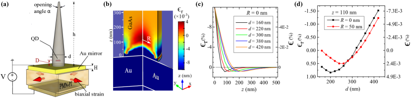
The design criteria to optimize both the coupling of the QD emission into the fundamental mode of a nanowire waveguide and the directionality of the far-field radiation are well established Friedler et al. (2009); Gregersen et al. (2008); Claudon et al. (2013). A reduced nanowire diameter () of 0.235 is found to optimally funnel the QD emission into the fundamental mode in both directions along a GaAs nanowire. A mirror terminates one end of the nanowire to reflect incident light towards the outcoupling nanowire end, where a conical taper is introduced to adiabatically expand the confined mode into a plane-wave in free-space. The angle of the conical tapering () determines both the reflection of the guided mode and the divergence angle of the far-field radiation pattern; for a QD located at the nanowire center, leads to (see Sec. SII in the Supplemental Material 111See Supplemental Material at [URL will be inserted by Publisher] for details on the fabrication procedure, determination of the experimental photon extraction efficiency as well as FDTD simulation of the structure.). Coupling of the light to the fundamental mode is optimised by placing the dot at the electric field’s antinode caused by the standing wave pattern between the mirror and emitter. An idealised sketch of our device is shown in Fig. 1 (a). It consists of a self-assembled QD located a distance from a Au mirror and radially centred in a nanowire with height , diameter , and taper angle . The Au mirror (with thickness = 200 nm) is deposited directly onto a single crystal lead magnesium niobate-lead titanate (PMN-PT) substrate (m thick) to also act as an electrical contact for piezoelectric bi-axial strain tuning. This top electrical contact is grounded to prevent large electric fields near the QD. The complete fabrication procedure is detailed in the Supplemental Material Note (1).
To better understand the challenge associated with strain tuning a QD in a high-aspect-ratio nanowire, we have simulated the complete device using finite element method (FEM) (Fig. 1 (b)-(d)). We quantify strain-field relaxation by means of the relative strain (), defined as , where is the strain at a given position with coordinates , and is the strain in the PMN-PT crystal. Fig. 1 (b) shows the profile of relative strain , with and nm. The colour legend is scaled to highlight the strain-field relaxation within the nanowire. In Fig. 1 (c), we show the plot of (and ) as a function of axial position along the nanowire for different diameters at the centre of the nanowire, nm. For nm, we also show the strain as a function of for radial positions nm, 50 nm in Fig. 1 (d). The modelling first confirmed that the strain relaxation is linear with respect to the applied strain, i.e., , for (which is within the range expected for a PMN-PT single crystal for an applied voltage of 0 -1 kV Herklotz et al. (2010); Kumar et al. (2011)). The model shows that the strain field generated by the piezoelectric crystal relaxes substantially () across the 200 nm-thick Au layer. We note that, although the inclusion of a silica spacer between the nanowire and the Au layer has been shown to increase modal reflectivityGregersen et al. (2008); Claudon et al. (2013), its absence in our device enhances strain transfer to the nanowire from the Au layer by based on our simulation results. The remaining strain field transmitted across the Au/GaAs interface is highly dependent on the diameter of the nanowire, as well as on the radial and axial position within the nanowire. In particular, we see increased relaxation with reducing nanowire diameter [Fig. 1 (c)] as well as higher strain fields nearer the centre of the nanowire [Fig. 1 (d)]. Although the applied strain is compressive, regions of tensile strain are seen as the strain relaxes along the nanowire. The axial position for optimal strain tuning is found to be in conflict with that required for optimal coupling to the mode. In fact, with geometry optimised for coupling at nm (i.e., nm, nm, nm), we obtain . While changing to nm significantly increases , it will likely lead to increased spectral fluctuations due to the effect of surface states at the mirror/nanowire interface Houel et al. (2012); Wang et al. (2004). Keeping nm and nm for nm, is maximised at nm before completely relaxing by nm. For a QD at nm and nm in a pillar with diameter nm, the model predicts a relative strain of while is only moderately affected (see Supplemental Material Note (1)), demonstrating the validity of the device as an efficient and elastically tunable platform for quantum photonics.
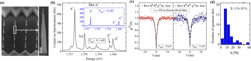
We have spectroscopically characterized numerous nanowires with constant (110 nm) and (2 m) but varying and . While the nanowires are not deterministically aligned to the randomly positioned QDs, the wafer has a suitably high QD density () for us to typically observe 3 to 5 spectrally isolated QDs per nanowire. A scanning-electron-microscope (SEM) image of an array of some of the brightest devices is shown in Fig. 2 (a), where nm (corresponding to for 920 nm 950 nm, the typical range of ground state exciton emission wavelengths for the QDs in this wafer), and .
PL spectra were acquired from the sample at K using a confocal microscope with a 0.82 NA objective lens. The QDs were excited non-resonantly (nm) using a continuous-wave (CW) laser diode. To maximize the PL signal we focused the collection optics at the top of the nanowire while the excitation laser was focused at the bottom of the nanowire. The PL was characterized using a spectrometer (0.5 m focal length and grating giving a resolution of eV [full width at half maximum (FWHM)] measured using a narrow-band laser) and a liquid-nitrogen-cooled Si charge-coupled-device (CCD) camera. Second-order correlation measurements were acquired using a Hanburry Brown-Twiss setup (eV spectral resolution) with two silicon single-photon avalanche diodes (timing jitter ps) and timing electronics.
The PL spectra from a QD (Dot A) found in one of the brightest wires is shown in Fig. 2 (b). The exciton states are identified by the characteristic Coulomb interactions observed in experiments with similar QDs in charge-tunable devices Dalgarno et al. (2008) and the linear (quadratic) power dependence for single (bi-) excitons. The spectra in Fig. 2 (b) are representative of what we typically observe from QDs in the nanowires, except with varying central energies and peak intensities. Further confirmation of the state assignment can be obtained by measuring the photon-intensity correlations between separate excitonic states Regelman et al. (2001). Figure 2 (c) shows the second order auto-correlation measurement of the state from another QD, Dot B. The raw data shows 0.5 while the fit to data deconvolved for detector jitter shows , signifying high-purity single-photon emission. The second order cross-correlation measurement between the and states (Fig. 2 (d)) also demonstrates clear antibunching, signifying that these states originate from the same QD Gerardot et al. (2005). Also, the absence of complex dynamics in the second-order correlation experiments demonstrates charge-state stability on short timescales Davanço et al. (2014); Santori et al. (2004).
The correct excitonic line assignment enables estimation of the total from a single dot, defined as the power collected into the objective lens divided by the power emitted by the QD. The latter can be estimated at saturation from the emission rates of each excitonic state (defined as the inverse of the transition’s lifetime) and the relative integrated intensities of each excitonic state. The efficiency of the experimental setup (from the objective lens to the CCD camera) was calibrated using a tunable laser at the QD emission wavelength. was thus estimated for the 40 brightest dots in the 16 nominally identical nanowires, as summarised in the histogram in Fig. 2 (d). We find for our brightest dot when each excitonic state is included, and . The most obvious explanation for the large standard deviation of is the random positioning of the dots radially in the nanowires, which could be remedied in the future with a deterministic positioning technique Gazzano et al. (2013). Additionally, the SEM images reveal surface defects and slight asymmetry in the nanowires, which may adversely affect performance. However, we are unable to correlate differences in particular structures with their brightness. Curiously, we have spectroscopically characterized numerous nanowire structures made from the same wafer with smoother features and better symmetry but worse .
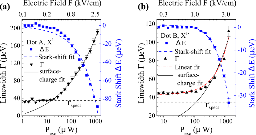
Non-resonant PL spectroscopy enables investigation of the effect of the nearby nanowire surfaces on the spectral linewidths and exciton energies of QDs. The non-resonant laser excites carriers above the GaAs band-gap that can relax into the QD as well as fill defect surface states; increasing the excitation power () increases the number of carriers at the nanowire surface. For the self-assembled InGaAs QDs investigated here, eV. Figs 3 (a) and (b) show the energy detuning () and measured linewidths () for the for Dots A and B, respectively. For W for Dot A, is zero and is resolution limited. For Dot B, is zero and is constant ( eV) but inhomogeneously broadened above the experimental resolution limit in the low power regime (W). For both QDs, as increases from the low power regime, increases and broadens without saturation. To better understand and quantify the effect of the surface states, we exploit the ability of the QD itself to function as an in-situ probe of the local electric field Gerardot et al. (2007); Vogel et al. (2007); Houel et al. (2012); Vamivakas et al. (2011). In an electric field, the quantum dot dipole manifests a Stark shift with quadratic field dependence, and the energy detuning is given by , where is the electric field, the permanent dipole moment, and the polarizability.
To gain physical insight, we express , where is the electronic charge, and is the electron-hole wave function separation.
To estimate at the position of the QD based on observed in PL measurements, we assume Gerardot et al. (2007); Vogel et al. (2007). The fits from this procedure give Å and Å for dots A and B respectively. The fits are shown as the dashed lines in Fig. 3, with the extracted values for shown on the top -axis in the figures. The fits agree well with the data and we observe that is linearly proportional to for each QD. Further, we can estimate the fluctuating electric field, , by assuming the fluctuation () in the number of electrons () located at the surface is proportional to the electronic shot noise: . We calculate by assuming electrons a distance /2 create , and then use to find the corresponding from the Stark equation. For Dot A, the estimated power broadening of (shown as the solid line labeled surface-charge fit in Fig. 3(a)) fits the experimental data very well above the system’s resolution limit. The surface-charge fit also enables us to estimate the power broadening below the resolution limit. Both the data and the extrapolated fit suggest the inhomogeneous broadening is dominated by the charges generated by the excitation laser at the nanowire surface. The results from Dot A are promising for the generation of indistinguishable photons from a QD in a nanowire antenna. On the other hand, a fit with a linear dependence of on is found to fit the data for Dot B much better than a surface-charge fit, even in the high regime. This result suggests that unlike the behavior of Dot A’s power broadening, Dot B’s linewidth broadening is not solely caused by the charge fluctuations generated at the nanowire surface by non-resonant excitation.
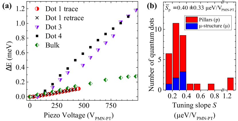
Finally, we demonstrate the elastic tunability of the exciton states. Fig. 4 (a) shows several examples of exciton detuning for QDs in different nanowire antennas as a function of applied bias to the piezoelectric crystal (). We observe varied strain-tuning slopes for each QD in each nanowire, as summarised for 30 QDs in the histogram in Fig. 4 (b). Also shown is a histogram of the strain tuning of QDs located in the roughly unetched region of the sample nearby the nanowires (-structure). This is partly visible in Fig. 2 (a) on the top and bottom edges of the array. In general, the strain tuning is achieved with small amounts of hysteresis, as shown for Dot 1. A maximum tuning amplitude of meV was achieved in the experiment. The large standard deviation in tuning is expected for two reasons: (i) the amplitude and even sign of the strain field is highly dependent on the radial position of the QD in the nanowire (as shown in Fig. 1); and (ii) strain tuning of the quantum states is highly dependent on the exact morphology of the dot, which is unique for every QD Sapienza et al. (2013); Kuklewicz et al. (2012); Jöns et al. (2011). In spite of the significant strain-field relaxation in the Au contact and the nanowire, we achieve substantial in-situ strain tuning of the QD excitonic transition energies. Further improvement in the tuning range can be obtained by reducing the Au layer thickness and moving the QD closer to the mirror, which may however lead to more spectral fluctuations.
In conclusion, we have demonstrated an elastically-tunable QD embedded in a nanowire waveguide emitting single photons with resolution-limited linewidths. The device enables strain tuning of excitons by up to 1.2 meV, which could enable resonant fluorescence experiments, reduction of fine-structure splitting for entangled photon-pair generation, and two-photon interference from separate QDs in nanowire antennas.
Acknowledgements: The authors would like to thank G.C. Ballesteros for assistance with FEM software (COMSOL), and acknowledge the financial support for this work from a Royal Society University Research Fellowship, the EPSRC (grant numbers: EP/I023186/1, EP/K015338/1), and an ERC Starting Grant (number: 307392).
References
- Santori et al. (2002) C. Santori, D. Fattal, J. Vučković, G. S. Solomon, and Y. Yamamoto, Nature 419, 594 (2002).
- Ates et al. (2009) S. Ates, S. Ulrich, S. Reitzenstein, A. Löffler, A. Forchel, and P. Michler, Physical Review Letters 103, 167402 (2009).
- He et al. (2013) Y.-M. He, Y. He, Y.-J. Wei, D. Wu, M. Atatüre, C. Schneider, S. Höfling, M. Kamp, C.-Y. Lu, and J.-W. Pan, Nature Nanotechnology 8, 213 (2013).
- Akopian et al. (2006) N. Akopian, N. H. Lindner, E. Poem, Y. Berlatzky, J. Avron, D. Gershoni, B. D. Gerardot, and P. M. Petroff, Physical Review Letters 96, tunable (2006).
- Salter et al. (2010) C. Salter, R. Stevenson, I. Farrer, C. Nicoll, D. Ritchie, and A. Shields, Nature 465, 594 (2010).
- De Greve et al. (2013) K. De Greve, P. L. McMahon, L. Yu, J. S. Pelc, C. Jones, C. M. Natarajan, N. Y. Kim, E. Abe, S. Maier, C. Schneider, M. Kamp, S. Höfling, R. H. Hadfield, A. Forchel, M. M. Fejer, and Y. Yamamoto, Nature Communications 4, 2228 (2013).
- Gao et al. (2012) W. Gao, P. Fallahi, E. Togan, J. Miguel-Sanchez, and A. Imamoglu, Nature 491, 426 (2012).
- Schaibley et al. (2013) J. Schaibley, A. Burgers, G. McCracken, L.-M. Duan, P. Berman, D. Steel, A. Bracker, D. Gammon, and L. Sham, Physical Review Letters 110, 167401 (2013).
- Press et al. (2008) D. Press, T. D. Ladd, B. Zhang, and Y. Yamamoto, Nature 456, 218 (2008).
- Brunner et al. (2009) D. Brunner, B. D. Gerardot, P. A. Dalgarno, G. Wüst, K. Karrai, N. G. Stoltz, P. M. Petroff, and R. J. Warburton, Science 325, 70 (2009).
- Knill et al. (2001) E. Knill, R. Laflamme, and G. J. Milburn, Nature 409, 46 (2001).
- Kok and Lovett (2010) P. Kok and B. W. Lovett, 1st ed. (Cambridge University Press, 2010).
- Kimble (2008) H. Kimble, Nature 453, 1023 (2008).
- Sangouard et al. (2011) N. Sangouard, C. Simon, H. de Riedmatten, and N. Gisin, Rev. Mod. Phys. 83, 33 (2011).
- Patel et al. (2010) R. B. Patel, A. J. Bennett, I. Farrer, C. A. Nicoll, D. A. Ritchie, and A. J. Shields, Nature Photonics 4, 632 (2010).
- Flagg et al. (2010) E. B. Flagg, A. Muller, S. V. Polyakov, A. Ling, A. Migdall, and G. S. Solomon, Physical Review Letters 104, 137401 (2010).
- Strauf et al. (2007) S. Strauf, N. G. Stoltz, M. T. Rakher, L. A. Coldren, P. M. Petroff, and D. Bouwmeester, Nature Photonics 1, 704 (2007).
- Gazzano et al. (2013) O. Gazzano, S. M. de Vasconcellos, C. Arnold, A. Nowak, E. Galopin, I. Sagnes, L. Lanco, A. Lemaître, and P. Senellart, Nature Communications 4, 1425 (2013).
- Madsen et al. (2014) K. H. Madsen, S. Ates, J. Liu, A. Javadi, S. M. Albrecht, I. Yeo, S. Stobbe, and P. Lodahl, Phys. Rev. B 90, 155303 (2014).
- Davanço et al. (2011) M. Davanço, M. Rakher, D. Schuh, A. Badolato, and K. Srinivasan, Applied Physics Letters 99, 041102 (2011).
- Trotta et al. (2012) R. Trotta, P. Atkinson, J. Plumhof, E. Zallo, R. Rezaev, S. Kumar, S. Baunack, J. Schroeter, A. Rastelli, and O. Schmidt, Advanced Materials 24, 2668 (2012).
- Ma et al. (2014) Y. Ma, P. E. Kremer, and B. D. Gerardot, Journal of Applied Physics 115, 023106 (2014).
- Claudon et al. (2010) J. Claudon, J. Bleuse, N. S. Malik, M. Bazin, P. Jaffrennou, N. Gregersen, C. Sauvan, P. Lalanne, and J.-M. Gérard, Nature Photonics 4, 174 (2010).
- Reimer et al. (2012) M. E. Reimer, G. Bulgarini, N. Akopian, M. Hocevar, M. B. Bavinck, M. A. Verheijen, E. P. Bakkers, L. P. Kouwenhoven, and V. Zwiller, Nature Communications 3, 737 (2012).
- Gregersen et al. (2008) N. Gregersen, T. R. Nielsen, J. Claudon, J.-M. Gérard, and J. Mørk, Optics Letters 33, 1693 (2008).
- Friedler et al. (2009) I. Friedler, C. Sauvan, J.-P. Hugonin, P. Lalanne, J. Claudon, and J.-M. Gérard, Optics Express 17, 2095 (2009).
- Claudon et al. (2013) J. Claudon, N. Gregersen, P. Lalanne, and J.-M. Gérard, ChemPhysChem 14, 2393 (2013).
- Finley et al. (2001) J. J. Finley, P. W. Fry, A. D. Ashmore, A. Lemaître, A. I. Tartakovskii, R. Oulton, D. J. Mowbray, M. S. Skolnick, M. Hopkinson, P. D. Buckle, and P. A. Maksym, Physical Review B 63, 161305 (2001).
- Högele et al. (2004) A. Högele, S. Seidl, M. Kroner, K. Karrai, R. J. Warburton, B. D. Gerardot, and P. M. Petroff, Physical Review Letters 93, 217401 (2004).
- Gerardot et al. (2007) B. D. Gerardot, S. Seidl, P. A. Dalgarno, R. J. Warburton, D. Granados, J. M. Garcia, K. Kowalik, O. Krebs, K. Karrai, A. Badolato, and P. M. Petroff, Applied Physics Letters 90, 041101 (2007).
- Vogel et al. (2007) M. Vogel, S. Ulrich, R. Hafenbrak, P. Michler, L. Wang, A. Rastelli, and O. Schmidt, Applied Physics Letters 91, 051904 (2007).
- Seidl et al. (2006) S. Seidl, M. Kroner, A. Högele, K. Karrai, R. J. Warburton, A. Badolato, and P. M. Petroff, Applied Physics Letters 88, 203113 (2006).
- Kuklewicz et al. (2012) C. E. Kuklewicz, R. N. Malein, P. M. Petroff, and B. D. Gerardot, Nano Letters 12, 3761 (2012).
- Sapienza et al. (2013) L. Sapienza, R. N. Malein, C. E. Kuklewicz, P. E. Kremer, K. Srinivasan, A. Griffiths, E. Clarke, M. Gong, R. J. Warburton, and B. D. Gerardot, Physical Review B 88, 155330 (2013).
- Gregersen et al. (2010) N. Gregersen, T. R. Nielsen, J. Mørk, J. Claudon, and J.-M. Gérard, Optics Express 18, 21204 (2010).
- Yeo et al. (2013) I. Yeo, P.-L. de Assis, A. Gloppe, E. Dupont-Ferrier, P. Verlot, N. S. Malik, E. Dupuy, J. Claudon, J.-M. Gérard, A. Auffèves, G. Nogues, S. Seidelin, J.-P. Poizat, O. Arcizet, and M. Richard, Nature Nanotechnology (2013).
- Montinaro et al. (2014) M. Montinaro, G. Wüst, M. Munsch, Y. Fontana, E. Russo-Averchi, M. Heiss, A. Fontcuberta i Morral, R. J. Warburton, and M. Poggio, Nano Letters 14, 4454 (2014).
- Weiß et al. (2014) M. Weiß, J. B. Kinzel, F. J. Sch lein, M. Heigl, D. Rudolph, S. Mork tter, M. D blinger, M. Bichler, G. Abstreiter, J. J. Finley, et al., Nano letters 14, 2256 (2014).
- Bouwes Bavinck et al. (2012) M. Bouwes Bavinck, M. Zielinski, B. J. Witek, T. Zehender, E. P. Bakkers, and V. Zwiller, Nano Letters 12, 6206 (2012).
- Houel et al. (2012) J. Houel, A. V. Kuhlmann, L. Greuter, F. Xue, M. Poggio, B. D. Gerardot, P. A. Dalgarno, A. Badolato, P. M. Petroff, A. Ludwig, D. Reuter, A. D. Wieck, and R. J. Warburton, Physical Review Letters 108, 107401 (2012).
- Berthelot et al. (2006) A. Berthelot, I. Favero, G. Cassabois, C. Voisin, C. Delalande, P. Roussignol, R. Ferreira, and J.-M. Gérard, Nature Physics 2, 759 (2006).
- Bounouar et al. (2012) S. Bounouar, A. Trichet, M. Elouneg-Jamroz, R. André, E. Bellet-Amalric, C. Bougerol, M. Den Hertog, K. Kheng, S. Tatarenko, and J.-P. Poizat, Physical Review B 86, 085325 (2012).
- Wang et al. (2004) C. Wang, A. Badolato, I. Wilson-Rae, P. Petroff, E. Hu, J. Urayama, and A. Imamoğlu, Applied Physics Letters 85, 3423 (2004).
- Davanço et al. (2014) M. Davanço, C. S. Hellberg, S. Ates, A. Badolato, and K. Srinivasan, Phys. Rev. B 89, 161303 (2014).
- Yeo et al. (2011) I. Yeo, N. S. Malik, M. Munsch, E. Dupuy, J. Bleuse, Y. M. Niquet, J. M. Gérard, J. Claudon, E. Wagner, S. Seidelin, A. Auffèves, J. P. Poizat, and G. Nogues, Applied Physics Letters 99, 233106 (2011).
- Reimer et al. (2014) M. E. Reimer, G. Bulgarini, R. W. Heeres, B. J. Witek, M. A. Versteegh, D. Dalacu, J. Lapointe, P. J. Poole, and V. Zwiller, arXiv preprint arXiv:1407.2833 (2014).
- Huber et al. (2014) T. Huber, A. Predojević, M. Khoshnegar, D. Dalacu, P. J. Poole, H. Majedi, and G. Weihs, arXiv preprint arXiv:1405.3765 (2014).
- Versteegh et al. (2014) M. A. Versteegh, M. E. Reimer, K. D. Jöns, D. Dalacu, P. J. Poole, A. Gulinatti, A. Giudice, and V. Zwiller, arXiv preprint arXiv:1405.4278 (2014).
- Note (1) See Supplemental Material at [URL will be inserted by Publisher] for details on the fabrication procedure, determination of the experimental photon extraction efficiency as well as FDTD simulation of the structure.
- Herklotz et al. (2010) A. Herklotz, J. D. Plumhof, A. Rastelli, O. G. Schmidt, L. Schultz, and K. Dorr, Journal of Applied Physics 108, 094101 (2010).
- Kumar et al. (2011) S. Kumar, R. Trotta, E. Zallo, J. Plumhof, P. Atkinson, A. Rastelli, and O. Schmidt, Applied Physics Letters 99, 161118 (2011).
- Dalgarno et al. (2008) P. A. Dalgarno, J. M. Smith, J. McFarlane, B. D. Gerardot, K. Karrai, A. Badolato, P. M. Petroff, and R. J. Warburton, Phys. Rev. B 77, 245311 (2008).
- Regelman et al. (2001) D. V. Regelman, U. Mizrahi, D. Gershoni, E. Ehrenfreund, W. V. Schoenfeld, and P. M. Petroff, Physical Review Letters 87, 257401 (2001).
- Gerardot et al. (2005) B. D. Gerardot, S. Strauf, M. J. A. de Dood, A. M. Bychkov, A. Badolato, K. Hennessy, E. L. Hu, D. Bouwmeester, and P. M. Petroff, Physical Review Letters 95, 137403 (2005).
- Santori et al. (2004) C. Santori, D. Fattal, J. Vučković, G. S. Solomon, E. Waks, and Y. Yamamoto, Phys. Rev. B 69, 205324 (2004).
- Vamivakas et al. (2011) A. N. Vamivakas, Y. Zhao, S. Fält, A. Badolato, J. M. Taylor, and M. Atatüre, Physical Review Letters 107, 166802 (2011).
- Jöns et al. (2011) K. Jöns, R. Hafenbrak, R. Singh, F. Ding, J. Plumhof, A. Rastelli, O. Schmidt, G. Bester, and P. Michler, Physical Review Letters 107, 217402 (2011).
Supplemental Material for
“A strain-tunable quantum dot embedded in a nanowire antenna”
SI Fabrication procedure
Our fabrication procedure is illustrated in Fig. S1. We use a wafer grown by molecular beam epitaxy (MBE) consisting of a nm Al0.65Ga0.35As sacrificial-etch layer followed by a m thick GaAs layer in which a layer of QDs is grown 110 nm from the surface. A 100 nm (Au) mirror is deposited by electron beam evaporation. After this, the wafer is flipped and bonded to a PMN-PT crystal with a 100 nm-thick Au layer using a thermo-compression bonding step at temperature and pressure and MPa respectively. Hydrochloric acid at is used to selectively etch the sacrificial layer, allowing removal of the substrate wafer. Next, an e-beam-lithography shadow mask is defined in a 220 nm layer of PMMA/MMA [Poly(methyl methacrylate)] for the 90 nm-thick Ni dry-etch mask deposited by e-beam evaporation.
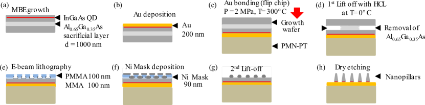
The PMMA/MMA is removed using acetone in an ultrasonic bath to expose the Ni discs which act as masks for the final dry-etching process.
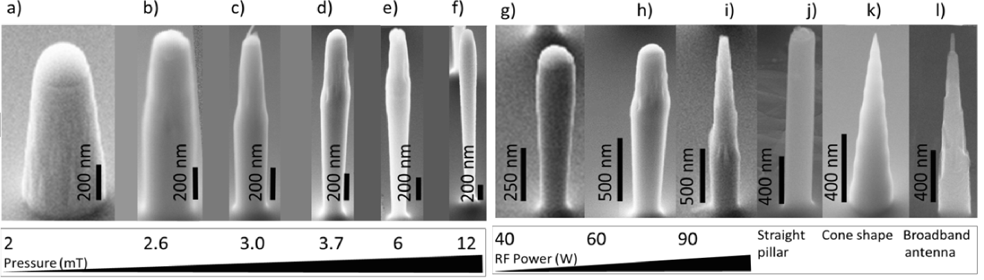
The dry-etching was carried out on an Oxford Plasmalab 100 ICP 65 system using a two-step process. A recipe for a straight etch (Tab. S1 col. (j)) followed by a recipe for controlled undercut of the mask (Table S1 col. (k)) resulted in the nanowires characterized in the manuscript.
| Parameter @ 20 | Straight (j) | Cone (k) |
|---|---|---|
| RF | 60 W | 90 W |
| ICP | 200 W | 150 W |
| Pressure | 8 mT | 2.7 mT |
| SiCl4/Ar | 7.5/15 sccm | 4/12 sccm |
To remove the remaining Ni and clean the taper from redeposited material, the sample was immersed in 1:10 Nitric acid:H2O for 2 minutes. The nitric acid treatment improved the taper angle by up to . Fig. S2 shows SEM images demonstrating the influence of dry etch parameters on the nanowire shape, i.e., RF power and RIE (reactive ion etch) gas chamber pressure.
SII Photon extraction efficiency
We perform finite-difference time-domain (FDTD) simulations (using Lumerical®) to model the performance of the nanowire antenna. The nanowire is characterised in terms of the following figures of merit: (1) The Purcell factor , which describes the enhancement or suppression of the spontaneous emission rate of the QD into a guided mode of the waveguide as compared with emission in bulk material. The Purcell factor can be moderately enhanced by adjusting the waveguide diameter to QD emission wavelength ratio and the dipole to mirror distance Friedler et al. (2009). (2) The mode-coupling efficiency or factor, which describes the fraction of photons emitted into the outcoupled mode in comparison with the total emission into all modes.
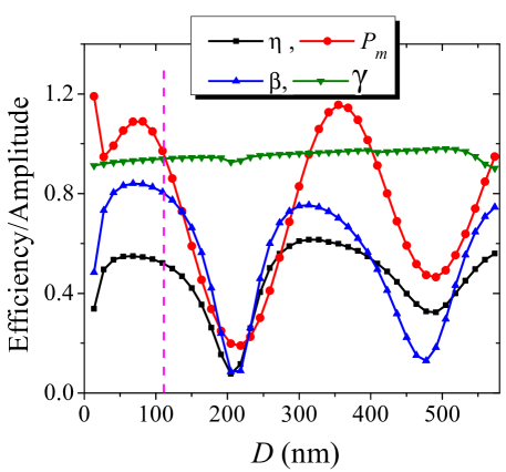
In the case of the only supported mode is the fundamental mode. (3) The extraction efficiency , which we define as the ratio of power emitted by the dipole and the power collected by the objective lens (with NA = 0.82 in our setup). (4) The collection efficiency , which is the ratio of light coupled out of the nanowire to that collected by the objective lens. Fig. S4 shows , , , and as functions of for nm, m, and , and an objective lens with NA of 0.82.
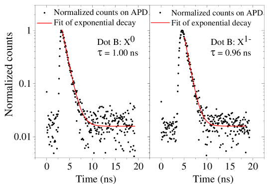
To experimentally determine the extraction efficiency of the nanowire (defined as the power collected into the objective lens divided by the power emitted by the QD), time-correlated single photon counting measurements of the excitonic transitions were performed. As mentioned in the main text, the power emitted by the QD at saturation is estimated from the emission rates of each excitonic state (defined as the inverse of the transition’s lifetime) and their relative integrated intensities. We assume ideal quantum efficiency for the QD. Our time-resolved measurements (see Fig. S4 and Fig. 2 (b) of the main manuscript) show charge state stability over short time scales and no evidence of complex dynamics, such as bi-exponential decay or bunching in autocorrelation measurements Santori et al. (2004); Davanço et al. (2014), while photoluminescence spectra demonstrate charge state stability over long time scales. The measurements of the and transitions for Dot B shown in Fig. S4 each reveal transition lifetimes of ns, approximately 10% to 20% longer than statistically expected for such dots Dalgarno et al. (2008). This is in agreement with the slight inhibition of spontaneous emission predicted by in Fig. S4.
References
- Friedler et al. (2009) I. Friedler, C. Sauvan, J.-P. Hugonin, P. Lalanne, J. Claudon, and J.-M. Gérard, Optics Express 17, 2095 (2009).
- Santori et al. (2004) C. Santori, D. Fattal, J. Vučković, G. S. Solomon, E. Waks, and Y. Yamamoto, Phys. Rev. B 69, 205324 (2004).
- Davanço et al. (2014) M. Davanço, C. S. Hellberg, S. Ates, A. Badolato, and K. Srinivasan, Phys. Rev. B 89, 161303 (2014).
- Dalgarno et al. (2008) P. A. Dalgarno, J. M. Smith, J. McFarlane, B. D. Gerardot, K. Karrai, A. Badolato, P. M. Petroff, and R. J. Warburton, Phys. Rev. B 77, 245311 (2008).