The Resistive-WELL detector: a compact spark-protected single amplification-stage MPGD
Abstract
In this work we present a novel idea for a compact spark-protected single amplification stage Micro-Pattern Gas Detector (MPGD). The detector amplification stage, realized with a structure very similar to a GEM foil, is embedded through a resistive layer in the readout board. A cathode electrode, defining the gas conversion/drift gap, completes the detector mechanics. The new structure, that we call Resistive-WELL (R-WELL), has some characteristics in common with previous MPGDs, such as C.A.T. and WELL, developed more than ten years ago. The prototype object of the present study has been realized in the 2009 by TE-MPE-EM Workshop at CERN. The new architecture is a very compact MPGD, robust against discharges and exhibiting a large gain (6103), simple to construct and easy for engineering and then suitable for large area tracking devices as well as huge calorimetric apparata.
keywords:
MPGD; Tracking and position sensitive detectors; Hadron Digital Calorimeter1 Introduction
The modern photolitographic technology on flexible and standard PCB supports has allowed the invention of novel and robust MPGDs, such as GEM [1], THGEM [2],[3] and Micromegas [4].
These detectors exhibit good spatial [5] and time [6] resolution, high rate capability [7], large sensitive area [8],
flexible geometry [9], good operational stability [10] and radiation hardness [11].
However, due to the fine structure and the typical micrometric distance of their electrodes, MPGDs generally suffer from spark occurrence that can eventually damage the detector.
The generation of the sparks in gas detectors is correlated with the transition from avalanche to streamer. This transition occurs when the Raether limit is overcome, that is when the primary avalanche size exceeds 107 - 108 ion-electron pairs [12].
In MPGDs, due to the very small distance between anode and cathode electrodes, the formation of the streamer can be easily followed by a discharge.
For GEMs the adopted solution is to share the gain among multiple amplification stages (double or triple-GEM structures), that allows a considerable reduction of the discharge rate [13],[14].
For Micromegas the problem of the spark occurrence between the metallic mesh and the readout PCB has been solved with the introduction of a resistive layer deposition realized on top of the readout itself [15]. The principle is the same of the resistive electrode used in Resistive Plate Counters (RPCs) [16],[17],[18]: the streamer, discharging a limited area around its location, is automatically quenched and the transition to spark is strongly suppressed giving the possibility to achieve large gains.
A further limitation of such MPGDs is correlated with the complexity of their assembly procedure. In particular, a GEM chamber requires some time-consuming assembly steps such as the stretching and the gluing of the GEM foils [19],[20],[21]. For this detector one of the co-authors of this paper has recently proposed a solution based on the so called NS2 assembly approach [22]: an evolution of the stretching technique introduced for the GEM chambers of the LHCb experiment [14].
Similar considerations can be also done for Micromegas, where the metallic mesh, defining the detector amplification region, requires a precise stretching.
The main goal of our project is the development of a novel MPGD by combining in a unique approach the solutions and improvements realized in the last years in the MPGD field:
a very compact detector structure, robust against discharges and exhibiting large gains (up to 104), easy to build, cost effective and suitable for mass production.
The novel detector, that we call Resistive-WELL (R-WELL), has some features (such as electric field shape and signal formation) in common with some MPGDs developed by the end of last century (C.A.T. [23] and WELL [24]). The prototype discussed in this work, designed at the Laboratori Nazionali di Frascati and realized in the 2009 by TE-MPE-EM Workshop at CERN, has been developed in parallel with the CERN-GDD group [25],[26].
2 Detector description
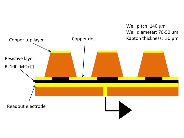
The R-WELL prototype, as sketched in fig. 2, is realized by merging a suitable etched GEM foil with the readout PCB plane coated with a resistive deposition. The copper on the bottom side of the foil has been patterned in order to create small copper dots in correspondence of each WELL structure. The resistive coating has been performed by screen printing technique, more sophisticated sputtering technology such as Diamond Like Carbon (DLC) can be used for precise resistive layer patterning.
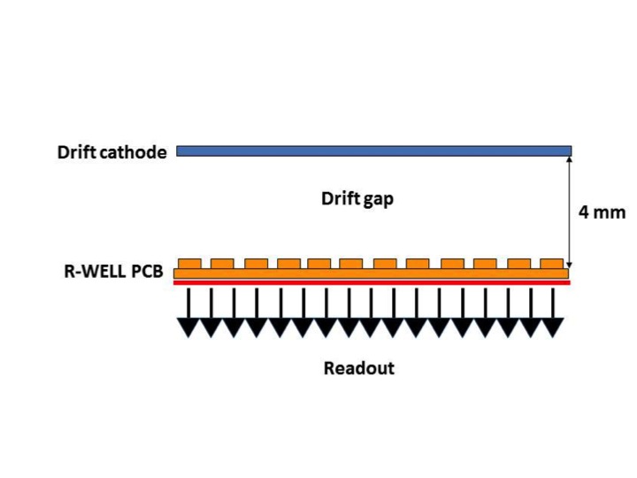
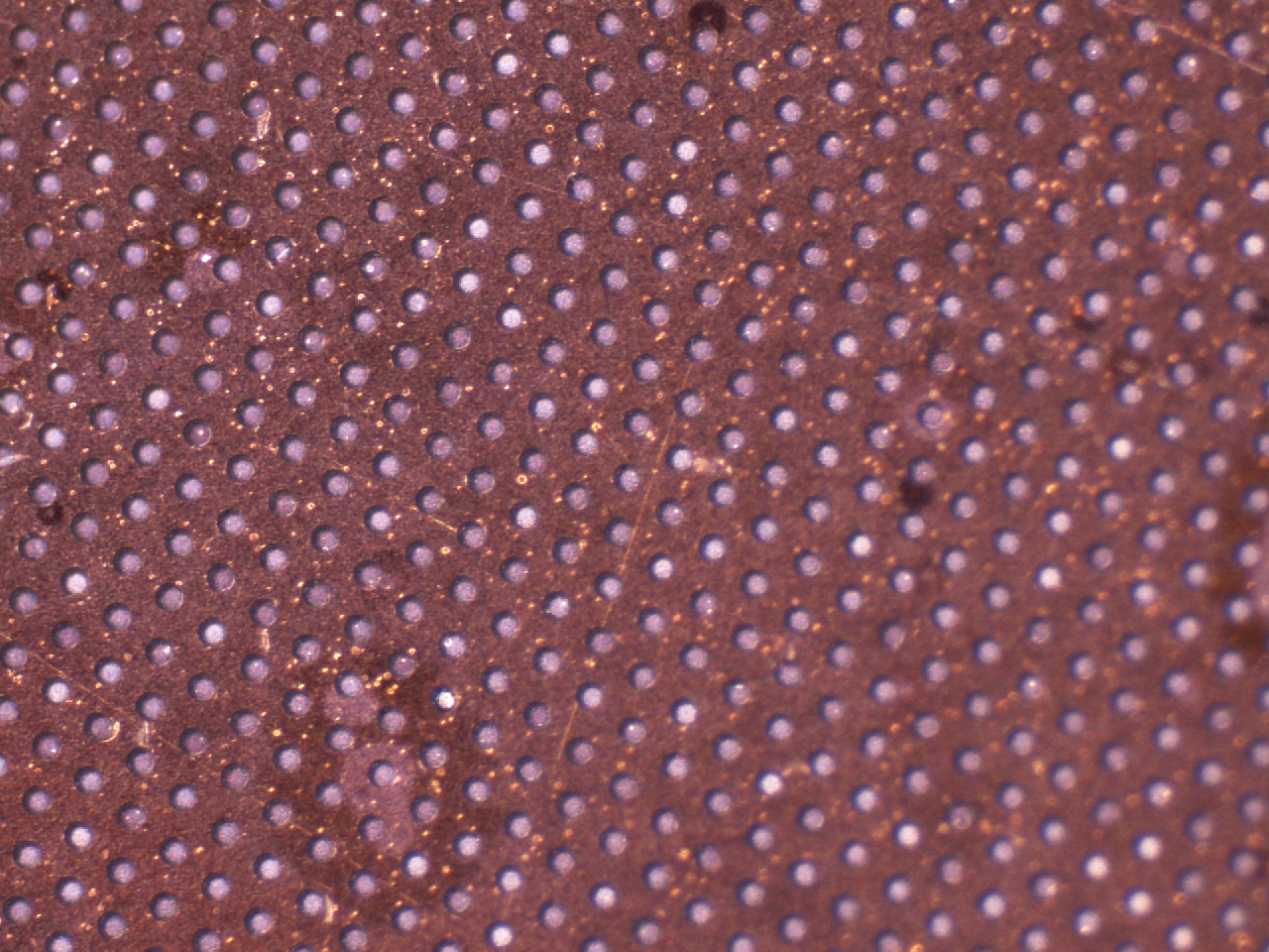
The WELL matrix is hence realized on a 50m thick polyimide foil, with conical channels 70m (50m) top (bottom) diameter and 140m pitch. A cathode electrode, defining the gas conversion/drift gap, completes the detector mechanics (fig. 2).
With respect to a classical single-GEM detector, the R-WELL is expected to exhibit a gas gain at least a factor of two larger.
Indeed in a single-GEM detector only 50% of the electron charge produced inside the holes contributes to the formation of the signal, while the rest of the electron charge is collected by the lower side of the GEM foil. In addition the signal in a GEM detector is mainly due to the electron motion, because the ion component is largely shielded by the GEM foil itself and the avalanche is confined in the holes.
In a R-WELL the whole electron charge produced into the amplification channel is promptly collected on the resistive layer (capacitively coupled with the readout plane) through the copper dot. Moreover also the ionic component, apart ballistic effects correlated with the integration time of the readout electronics, contributes to the formation of the signal in a similar way as the electron part.
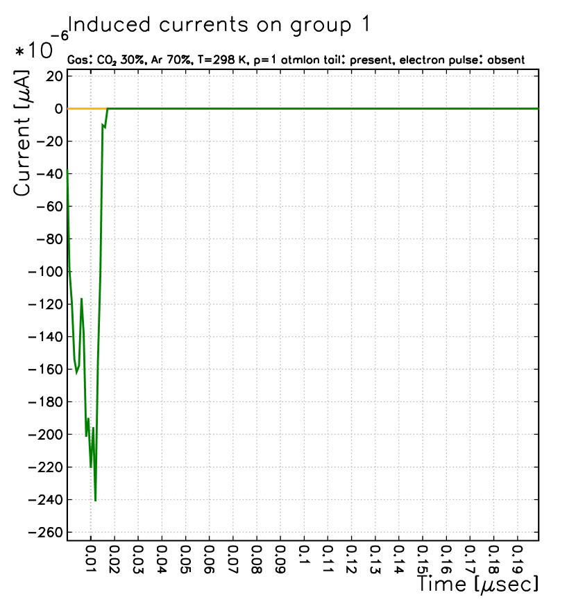
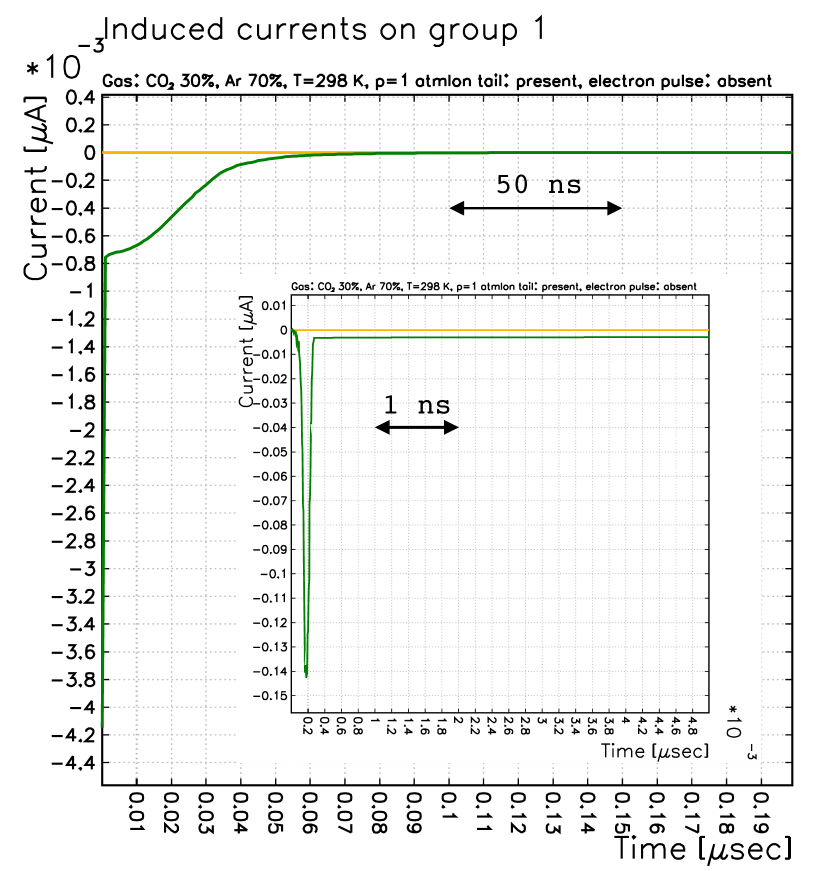
In fig. 4 and fig. 4 a comparison between the simulation of the signal generated by a single ionization electron in a single-GEM and a R-WELL is reported. In the R-WELL a further increase of the gain could be achieved thanks to the resistive electrode which, quenching the discharges, allows a higher amplification field inside the channel.
A distinctive advantage of the proposed technology is that the detector, composed by very few components, does not require complex and time-consuming assembly procedures: neither stretching, nor gluing, nor internal support frames are required.
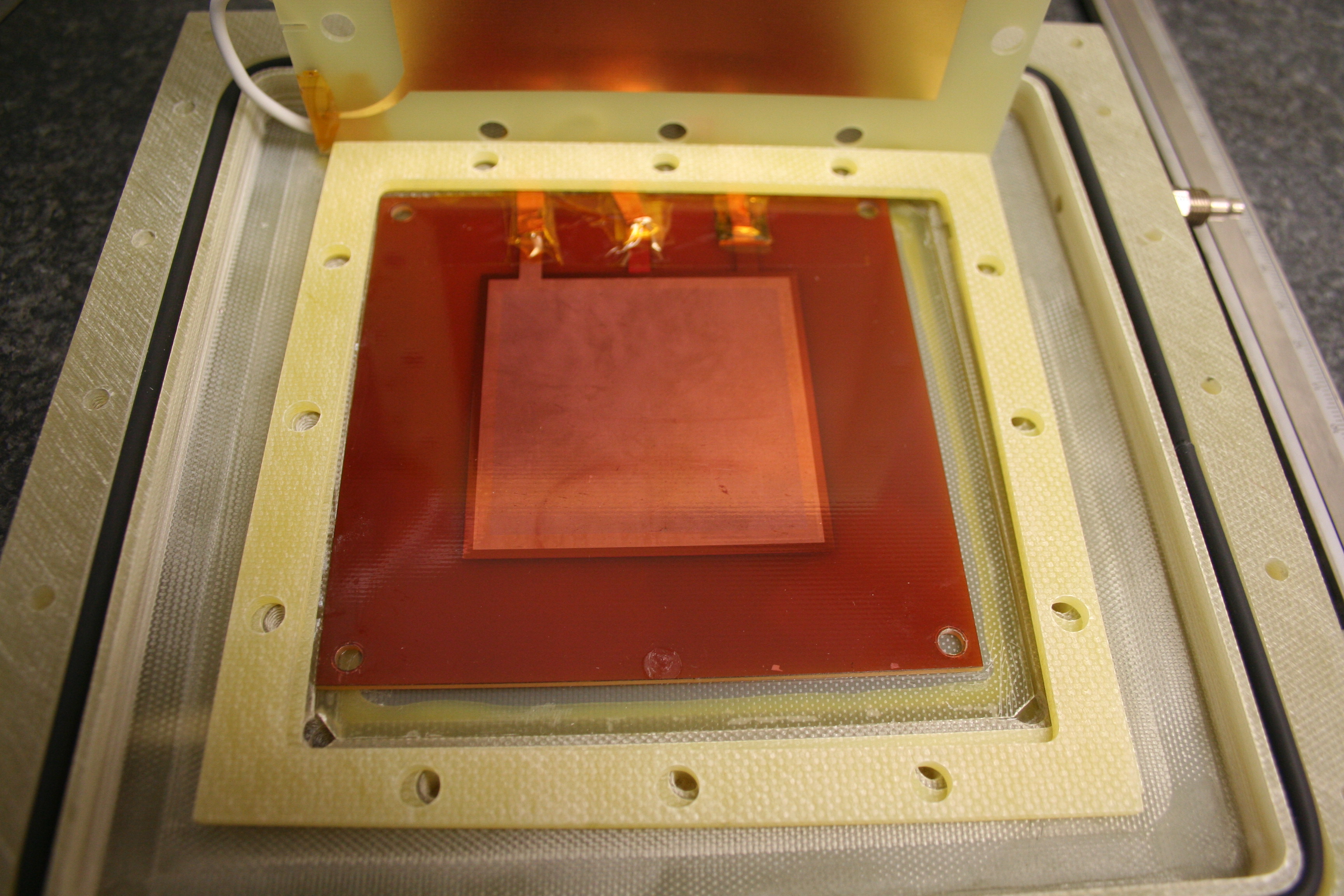
The prototype described in this paper has a 55 cm2 active area and the layer surface resistivity is 100 . The coating of the PCB has been realized by a polymer resistive paste deposition using the screen printing technique. The readout electrode has been realized as a unique pad as large as the detector active area. In figg. 6, 6 some details of the R-WELL PCB and the prototype are respectively shown.
3 Detector performance
The detector has been characterized by measuring the gas gain, rate capability and discharge behaviour in current mode, that is by recording the current drawn by the resistive layer under irradiation. The device has been irradiated with a collimated flux of 5.9 keV X-rays generated by a PW2217/20 Philips. The detector gain has been measured as a function of the potential applied between the top electrode of the amplification stage and the resistive layer (see fig. 2). For the measurement a Keithley-6485 pico-ammeter with 10 fA sensitivity has been used.
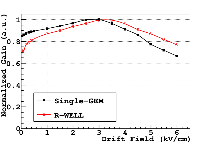
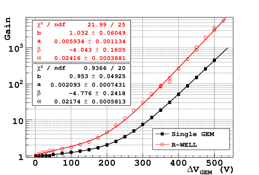
In a structure like the one discussed in this paper (as well as for a GEM) some of the field lines in the conversion/drift region are expected to terminate on the metallized layer of the upper part of the amplification stage. Primary electrons following these lines are not collected into the WELL (hole) and therefore are not multiplied, producing a collection inefficiency. As shown in fig. 8 the collection efficiency (estimated from the normalized gain [27]), for a fixed value of the voltage applied to the WELL (hole) structure, depends on the drift field. For the prototype studied in this work the maximum collection efficiency has been found in correspondence of a drift field of about 3.5 kV/cm (3.0 kV/cm for the single-GEM). As reported in fig. 8 the maximum gain achievable with the R-WELL (G6000 at V525 V) is significantly higher than that one exhibited by a standard single-GEM used as reference (G1000 at V500 V)111The gain has been parametrized as follows: .
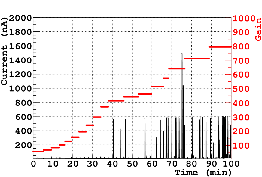
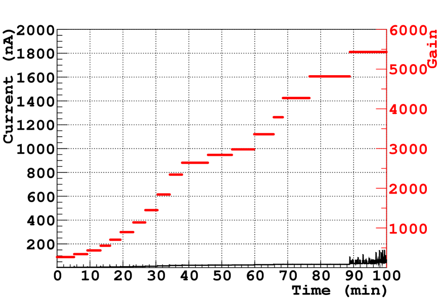
For both detectors the maximum voltage achieved during the measurement is correlated with the onset of the discharge activity, that, from a very qualitative analysis, comes out to be substantially different for the two devices. As shown in fig. 10 and fig. 10, the typical discharge amplitude for the R-WELL is of the order of few tens of nA (in anycase less than 100 nA also at the maximum gain), while for the GEM discharges with amplitude of the order of A are observed at high gas gain. Further systematic and more quantitative studies on this item must be clearly performed.
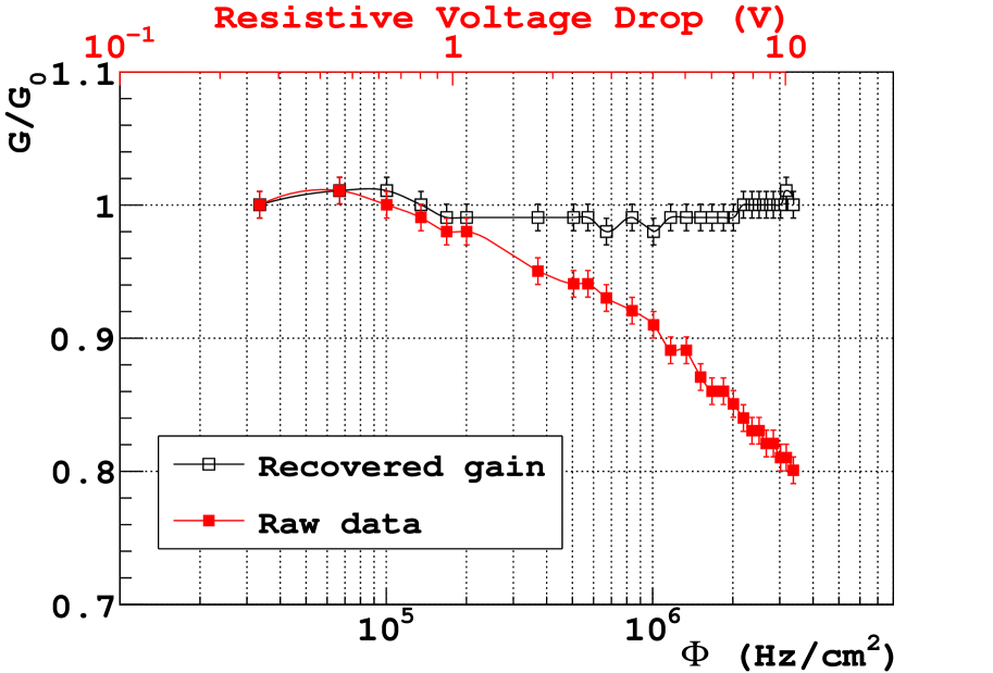
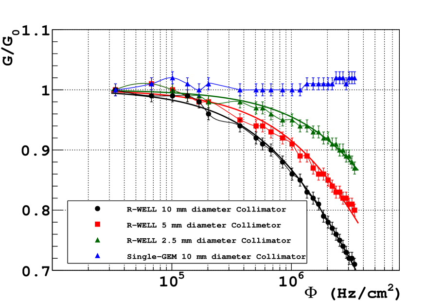
On the other hand a drawback correlated with the introduction of a high resistivity layer between the amplification stage and the readout is the reduced capability to stand high particle fluxes: larger the radiation rate, higher is the current drawn through the resistive layer and, as a consequence, larger the drop of the amplifying voltage (fig. 12). In fig. 12 the normalized gain of the single-GEM is compared with that obtained for the R-WELL with three different collimator diameters: 10 mm, 5 mm and 2.5 mm. The gain of the GEM is substantially constant over the explored range of radiation flux (up to 3 MHz/cm2), while the maximum particle flux that the R-WELL is able to stand, in agreement with an Ohmic behavior of the detector (see appendix A), decreases with the increase of the effective diameter of the X-ray spot on the detector. The points in fig. 12 are fitted with the function
| (1) |
for reasons explained in appendix A. The function 1 has been used to evaluate the radiation flux when the detector is expected to have a gain drop of 3%, 5% and 10% for all the collimators. These results, as shown in fig. 13, seem to indicate that the rate capability of the detector, for a fixed surface resistivity, can be tuned with a suitable segmentation of the resistive layer by means a conductive grid or with an equivalent current evacuation scheme.
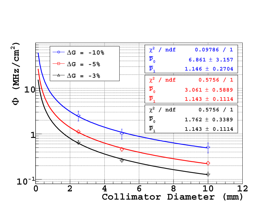
In addition, taking into account the higher ionization of the X-rays used in this measurement (210 electron-ion pairs), for m.i.p. (30 electron-ion pairs in 4 mm drift gap) the rate capability is expected to be larger of a factor 7. As a consequence, with a proper segmentation of the resistive layer, a rate capability of 1 MHz/cm2 for m.i.p seems to be achievable.
4 Conclusions
The R-WELL detector investigated in this work shows several advantages: small thickness (few millimeters), effective spark quenching, very simple assembly procedure, besides of good gas gain (G6000) and rate capability ranging for X-rays from 100 kHz/cm2 to 600 kHz/cm2 (G2000 and a surface resistivity of about 100 M). Larger gas gain could be achieved using thicker kapton foils for the realization of the R-WELL structure (polyimide foils with a thickness up to 125 m are produced from KANEKA ltd in Japan). Higher rate capability could be obtained using a suitable segmentation of the resistive layer and adjusting its surface resistivity. All these features make the R-WELL detector a valuable solution for large size tracking and calorimetric apparata where reliability, construction simplicity and cost-effective technology are recommendable.
Appendix A The gain drop in a R-WELL
The experimental data reveal that the gain variation of a R-WELL depends on the radiation flux (fig. 12) and the observed drop is supposed to be due to the resistive layer of the detector as explained in the following. The gain of a R-WELL can be written as a function of the potential difference applied on the amplification stage:
| (2) |
A gain drop corresponds to a decrease of the voltage
| (3) | |||||
Assuming that the gain drop is only due to the resistive layer we can write the Ohm’s first law
| (4) |
where is the current measured on the resistive layer and is the average resistance faced by the charges to reach the ground frame. The current can be written as follows
with the electron charge, is the number of electrons produced by a single photon (from GARFIELD simulations we have ), is the gain of the GEM foil and is the conversion rate of the X-ray in the gas. The rate can be also expressed in terms of a flux standing the simple relation , with the collimator radius. Eq. 3 becomes
The exponential can be expanded using the Maclaurin series up to the first order since the exponent is smaller than 1.
re-writable as
We insert the parameter defined as
| (5) |
which lets us write the solution of eq. A in a very simple way:
| (6) |
where the only positive solution is taken since the argument under square root is larger than 1.
Eq. 6 gives the ratio of to as a function of the X-rays flux and it has been used to fit the graphs in fig. 12.
Appendix B A model for the resistance : circular approximation
According to eq. 5, the relation between the parameter and the average resistance is given by
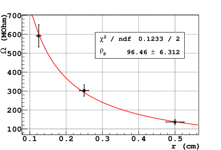
The dependence on the collimator radius is shown in fig. 14. We propose in the following a simplified model exploiting this dependence.
Let’s consider the axis of the collimator pointing to the center of the resistive layer and let be the half of side length of the active area and the collimator radius. We consider the case , so that we can approximate the active area as a circle with radius . The charge produced at a distance from the center will cover the path . The average path can be evaluated as follows:
| (7) | |||||
So we can consider that all the charge produced in the area is concentrated in the circle with radius . From that point the charge moves towards the ground frame ideally in a pipe with height (the thickness of the resistive layer) and width , with this width constant all over the path. Under this assumption the total surface crossed by all the charge is
| (8) |
According to the second Ohm’s law, using the results in 7 and 8, the average resistance is
| (9) | |||||
where we used the definition of surface resistivity .
References
- [1] F. Sauli, GEM: A new concept for electron amplification in gas detectors., Nucl. Inst. & Meth. A 386 (1997) 531.
- [2] L. Periale et al., Detection of the prymary scintillation light from dense Ar, Kr and Xe with novel photosensitive gaseous detectors., Nucl. Inst. & Meth. A 478 (2002) 377.
- [3] R. Chechik et al., Thick GEM-like multipliers - a simple solution for large area UV-RICH detectors., Nucl. Inst. & Meth. A 553 (2005) 35.
- [4] I. Giomataris et al., Micromegas: a high-granularity, position sensitive gaseous detector for high particle flux environments., Nucl. Inst. & Meth. A 376 (1996) 29.
- [5] B. Ketzer et al., Performance of triple GEM tracking detectors in the COMPASS experiment, Nucl. Instr. & Meth. A 535 (2004) 314.
- [6] M. Alfonsi et al., The triple-GEM detector for the M1R1 muon station at LHCb, IEEE NSSMIC Vol. 2 (2005) 811.
- [7] M.Poli Lener, Triple-GEM detectors for the innermost region of the muon apparatus at the LHCb experiment, Ph.D Thesis, XVIII cycle (2005), University of Rome ”Tor Vergata” , CERN-THESIS-2006-013.
- [8] D. Abbaneo et al., GEM based detector for future upgrade of the CMS forward muon system, Nucl. Instr. & Meth. A 718 (2013) 383.
- [9] A. Balla et al., The cylindrical GEM detector for the KLOE-2 Inner Tracker, JINST 9 C01014 (2014).
- [10] A. Cardini et al., The operational experience of the triple-GEM detectors of the LHCb muon system: Summary of the 2 years of data taking, IEEE NSS Conf. Record (2012) 759.
- [11] M. Alfonsi et al., Studies of etching effects on triple-GEM detectors operated with CF4-based gas mixtures, IEEE Trans. Nucl. Sci. 52 (2005) 2872.
- [12] H. Raether, Electron Avalanches and Breakdown in gases, Butterworth, London, 1964.
- [13] F. Sauli, Discharge studies and prevention in the gas electron multiplier, CERN-EP/2000-151, 11 December 2000.
- [14] M. Alfonsi et al., High-rate particle triggering with triple-GEM detector, Nucl. Inst. & Meth. A 518 (2004) 106.
- [15] P. Fonte et al., Advances in the Development of Micropattern Gaseous Detectors with Resistive Electrodes, Nucl. Inst. & Meth, A 661 (2012) 153.
- [16] Y. Pestov et al., A spark counter with large area, Nucl. Instr. & Meth. 93 (1971) 269.
- [17] R. Santonico, R. Cardarelli, Development of Resistive Plate Counters, Nucl. Instr. & Meth. A 377 (1981) 187.
- [18] M. Anelli et al., Glass electrode spark counters, Nucl. Instr. & Meth. A 300 (1991) 5072.
- [19] C. Altunbas et al., Construction, test and commissioning of the triple-GEM tracking detector for COMPASS., Nucl. Inst. & Meth. A 490 (2002) 177.
- [20] G. Bencivenni et al., A triple-GEM detector with pad readout for high rate charged particle triggering., Nucl. Inst. & Meth. A 488 (2002) 493.
- [21] G. Bagliesi et al., The TOTEM T2 telescope based on triple-GEM chambers., Nucl. Inst. & Meth. A 617 (2010) 134.
- [22] D. Abbaneo et al., GEM based detector for future upgrade of the CMS forward muon system, Nucl. Inst. & Meth. A 718 (2013) 383.
- [23] F. Bartol et al., The C.A.T. Pixel Proportional Gas Counter Detector, J. Phys. III France 6 (1996) 337.
- [24] R. Bellazzini et al., The WELL detector, Nucl. Inst. & Meth. A 423 (1999) 125.
- [25] M. Alfonsi et al., Performance measurements on closed-geometry GEM like detectors, presented at the MPGD2009 - 1st International Conference on Micropattern Gaseous Detectors, 12-15 June 2009 - Crete.
- [26] G. Croci, Development and characterization of Micro-Pattern Gaseous Detectors for HEP applications and beyond, Ph.D Thesis, XXIII cycle (2010), University of Siena.
- [27] S. Bachmann et al., Charge amplification and transfer processes in the gas electron multiplier, Nucl. Inst. & Meth. A 438 (1999) 376.