Grain Size and Lattice Parameter’s Influence on Band Gap of SnS Thin Nano-crystalline Films
Abstract
The parameters influencing the band gap of tin sulphide thin nano-crystalline films have been investigated. Both grain size and lattice parameters are known to influence the band gap. The present study initially investigates each contribution individually. The experimentally determined dependency on lattice parameter is verified by theoretical calculations. We also suggest how to treat the variation of band gap as a two variable problem. The results allow us to show dependency of effective mass (reduced) on lattice unit volume.
1 Introduction
The photovoltaic industry has been growing rapidly over the recent years due to the increasing demand for low cost and yet high efficiency solar cells. Tin Sulfide (SnS), a IV-VI group semiconductor having orthorhombic double layered structure with weak Van der Waals bonds between the layers, is considered a potential candidate due to its properties like high absorption coefficient () and band gap (of the order of ) [1, 2]. SnS films are amphoteric in nature, i.e., they can exist either as ‘n’-type or ‘p’-type depending on the fabrication conditions [3, 4]. SnS properties are also anisotropic [5, 6, 7] which along with its amphoterism demands an extensive investigation into its properties.
We have noticed that the orientation with which SnS films are fabricated depends on the substrate it is grown on. This in turn influences the lattice parameters. The grain size of the films showed thickness dependence. This allowed us to study the properties of SnS thin films, such as band gap, as a function of grain size and lattice parameters. We are hence in a position to experimentally comment on the effective mass of the charge carriers. Finally, we have compared our experimental results with the theoretical calculations made.
2 Experimental
Thin SnS films of varying thicknesses were fabricated by thermal evaporation of SnS pellets on optically flat glass and ITO substrates (150 nm thick layer of Indium tin oxide grown on glass substrate) maintained at room temperature using a Hind High Vac (12A4D) thermal evaporation coating unit at vacuum better than Torr. The starting material was 99.99% pure SnS powder provided by Himedia (Mumbai). The thickness of the films were measured using Dektak surface profiler (150). The structural analysis of the samples were done using X-ray Diffractometer (Bruker D8 X-ray Diffractometer) operating at 40 KV, 40 mA with radiation (λ=1.5406 Å) and Transmission Electron Microscopy (Technai T30U Twin). The optical absorption and transmission spectra of the films were recorded using an UV-Vis Double Beam Spectrophotometer (Systronics 2202) over the range of 300-1000 nm. The slow evaporation rate ensured the films were essentially defect free and exhibited a n-type conductivity, as was confirmed by Hot-probe measurements.
3 Results and Discussion
3.1 The Structural and Morphological Analysis
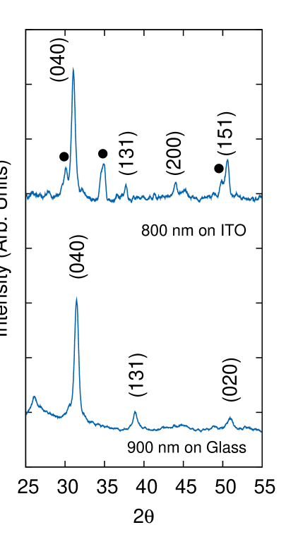
In this study, we have compared n-type SnS films grown on glass and ITO substrates of different thicknesses. The X-Ray Diffraction (XRD) profile for two comparable thicknesses are shown in fig. 1. The nature of pattern remained the same for increasing thickness with only exception in case of films fabricated on ITO substrates where the ITO peaks contribution decreased with increasing thickness. Both diffraction patterns matched well with the orthorhombic structure reported in ASTM card 83-1758 which reports the lattice parameters as a=4.148Å, b=11.48Å and c=4.177Å. However, the diffraction peaks corresponding to the (040), (131) and (020) planes were prominent for films grown on glass substrates while the films on ITO substrates shows the peaks corresponding to the (040), (131), (200) and (151) planes.

To investigate further, we have studied the samples using High Resolution Transmission Electron Microscope (HRTEM). The HRTEM images of SnS film on glass and ITO substrates are shown in fig. 2. The layered structure of the films is evident from the parallel lines seen. The interplanar distances can be directly measured from these images. The interplanar distance can also be calculated from XRD data using the formula [8]
| (1) |
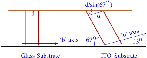
where a, b, c are the lattice parameters and h, k, l are the Miller indices given in the ASTM card. The interplanar distances evaluated from HRTEM micrographs of samples grown on glass were found to be around 0.285 nm. Considering that , this would imply that the lines seen in the micrograph are SnS layers arranged in the ‘ac’ plane with ‘b’ axis parallel to the substrate, or we may say our films have preferred orientation with the (040) planes perpendicular to the substrate. This orientation promises to be mechanically stable [9]. However, inter-planar distances measured from the micrographs of samples grown on ITO substrates are . This is due to the ‘ac’ planes making an angle of caused by the ‘b’ axis making an angle of with respect to the substrate (see fig 3).
Other then exhibiting polycrystallinity, fabricated films also exist in a state of stress, as is evident from the compressions or elongations experienced by the lattices. The lattice are said to be in a state of stress, also refered as “residual stress”. Residual stress are remanent unbalanced forces existing in the lattice due to the rapid condensation of material during film fabrication, or due to curvatures on the substrate and/or due to film-substrate interface etc. Residual strain can be evaluated from the displacement of the X-ray diffraction peaks from which lattice parameters are then evaluated. The lattice strain is given as [10]
| (2) |
where ‘l’ is the lattice parameter of the observed (subscript ‘’) and single crystal (subscript ‘’) sample. Using the values of the elastic constants, stress can be calculated using the strain values. We have calculated the lattice parameters for all our samples and shall comment on their significance subsequently.
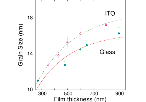
To investigate the variation of grain size with substrate and film thickness, we have calculated the average grain size of the films. The calculation were made using the Full Width at Half Maxima (FWHM) of the XRD peaks in the Scherrer’s formula [2, 8, 11]
| (3) |
where ‘r’ is the grain size, is the FWHM, and have their usual meanings. The grain sizes were found to vary from 11 to 18 nm depending on the film thickness in both substrates. However, it is clear from fig. 4 that for comparable film thickness we get larger grains of SnS on ITO substrates. Devika et al [12] have argued that SnS nucleation is easier on ITO compared to glass because of its crystalline nature.
We have observed that SnS films on glass substrates have the same values for ‘b’ and ‘c’ as in single crystal. However a tensile stress exists along the ‘a’ direction (i.e. ). In contrast to this, samples on ITO showed a compression along the ‘c’ direction which within experimental limits is constant for all film thicknesses. The lattice parameter ‘b’ remained equal to that of single crystal. Similar to the case of films on glass, here also a tensile stress existed along the ‘a’ axis. To summarize, SnS films grown on ITO have an exagerated tensile force acting along the ‘a’ direction and compressive forces acting along the ‘c’ direction resulting from the ‘b’ axis not being parallel to the ITO substrate. This, hence, gives us an opportunity to study the properties of SnS films and look into how variation in grain size, lattice parameter and orientation manifests itself on them.
3.2 Optical Analysis
The optical properties of a material are represented by its band gap and refractive index. Both these informations are evaluated from the UV-visible absorption/ transmission spectra. The absorption coefficient (‘’) is calculated followed by which using the standard Tauc method [13] the band gap of films are obtained by extrapolating the linear part of vs plot to the ‘X’-axis. The variation of band gap with grain size of SnS films grown on ITO and glass substrates are shown in fig. 5. Though the trends are similar, the absolute values are different possibly due to the different crystal orientation or lattice paramter, i.e. crystallinity, stress and orientation effect band gap values [6, 14, 15]. The trend follows [16]
| (4) |
or
| (5) |
where is the band gap of SnS in bulk, ‘’ and ‘’ are the effective mass of electron and holes, respectively.
This result is consistent with properties induced by quantum confinement of charge carriers [16]. Again this result confirms that SnS grains of 11-25 nm are in the nano-regime.
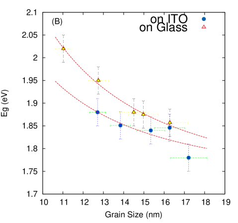
It would appear that the SnS grains with size greater than 25 nm would have band gap similar to the bulk. Curve fits to the data points of fig. 5 give for glass and ITO as 1.707 and 1.65 eV respectively. We believe the difference in value is a result of the different orientations in which the SnS film exists on glass and ITO substrates. The above data also allows us to explore variation in effective mass along different directions of SnS crystal. We however, can only comment on the reduced effective mass () using our experimental data. The reduced effective mass from curve fitting is and for samples on glass and ITO substrates respectively, where is the rest mass of free electron.
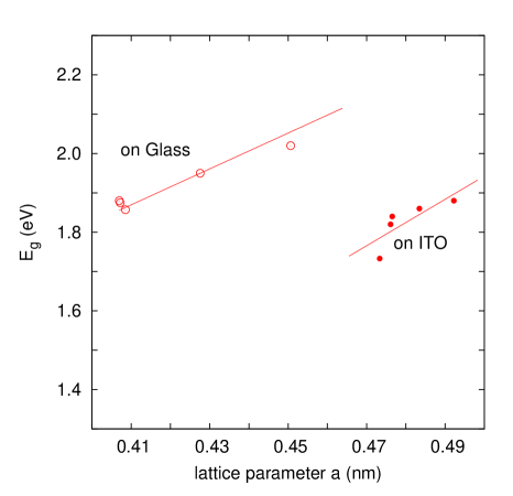
As can be seen from Fig. 6, the band gap of SnS thin films increases with increasing lattice parameter ‘a’. As explained by eqn (2), an increase in lattice parameter is indicative of a stress acting along ‘a’. Fig 6 shows that the stress is more in films fabricated on ITO substrates [17]. The difference in strain () stems from the difference in orientation between the films on different substrates. The data points from both the substrates do not lie on a single line. This is indicative of the fact that SnS band gap depends on the lattice parameter and a second variable, possibly the grain size (from fig 5). Experimentally, the different substrate used and variation in film thickness allowed us to control the two “variables”. Theoretically, however, we can only study the variation of band gap as a function of lattice parameters (or in other words unit cell volume). In the next section we investigate the results of fig 6 using theoretical calcultions.
4 Band Structure Calculation
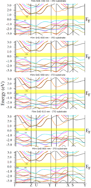
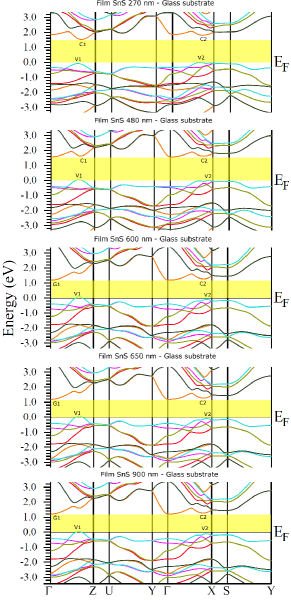
The band structure of SnS has been theoretically evaluate quite extensively [7, 9, 10, 18, 19]. We have performed ab initio calculations of the SnS electronic band structure in the framework of the density functional theory (DFT) as implemented in the WIEN2k software [20], adopting the Engel-Vosko approximation for the exchange-correlation potential. We analyzed the energetic behavior of the compound with the inclusion of the spin orbit interaction. For the calculations we have used the lattice parameters obtained experimentally for the various SnS films with 4 Sn and 4 S atoms (8 atoms) per unit cell, forming two parallel zigzag chains. To achieve total convergence in the self-consistent calculations, we used RKMAX equal to 7, and a converged sampling of 194 k-point in the first Brillouin Zone (BZ).
4.1 Structure of SnS for various lattice parameters
As stated in the preceeding section, we had deposited SnS films on ITO and glass substrates. We experimentally determined the lattice parameters for these samples. Using these lattice parameters, we computed the band structure of SnS thin films (Fig. 7). Since the lattice parameter ‘b’ showed insignificant variation with thickness in samples grown on glass and ITO substrates, we conclude that ‘b’ lattice parameter does not contribute to the variation in band gap. Also, its contribution is only along the direction of the BZ [7] where the “energy difference” (difference in valence band maximum and conduction band minimum) is too large to be considered as energy band gap associated with SnS.
However, many other valence band maximas and conduction band minimas are visible in the and . In fact, in one of the author’s previous studies [19] it was demonstrated that SnS and their related IV-VI orthorhombic compounds exhibit several direct and indirect gaps which are close in energy and competing to form the band gap. This makes it difficult to precisely determine whether the band gap is direct or indirect (confirmed by experimental works also [22, 23, 24]). Careful analysis of Fig. 7 show two comparable energy differences each contributing to the energy band gap of SnS films on glass and ITO substrates respectively. The calculated band gaps are smaller than the experimental ones due to the well known underestimation that DFT provides. This, however, can be overcomed by including the many-body electron-electron interaction, within the GW Hedin and Lundskvit [25, 26] formalism. We have previously calculated this correction for the semiconductor SnS [27], obtaining a constant potential value of 0.38 eV giving a good agreement with the experimental values. We have added this correction to all the calculated band gaps.
In SnS films grown on ITO substrates, the smallest “energy difference” is the indirect gap between the G1 maximum valence band at point and the minimum conduction band at C1, located at about 1/4 from the Z point. The second energy gap is a quasi-direct energy gap formed between the V1 relative maximum in the valence band, and the same minimum of the conduction band at C1. Both gaps are approximately equal and show the same variation with the normalised lattice’s unit cell volume (fig 8). For obtaining the normalised lattice’s unit cell volume, the stressed lattice’s unit volume is divided by the volume listed in the given ASTM Card (henceforth lattice’s unit cell volume would imply normalised lattice’s unit cell volume).
The films on glass substrates also show two important energy gaps, they are quasi-direct, one along along the direction of the BZ that occurs at 1/4 from Z point and second along the direction of the BZ. The variation of band gap with lattice’s unit cell volume is shown in fig (8). In fig (8), we have included the experimental data also (black solid and dashed trendlines are for SnS films on glass and ITO substrates respectively). Considering that the experimental method adopted to evaluate band gaps can not resolve the and contributions, the average of the band gaps calculated along the and directions also compared with those of the experimental data. The trendlines (slope) matched well (not shown in fig 8 for brevity).
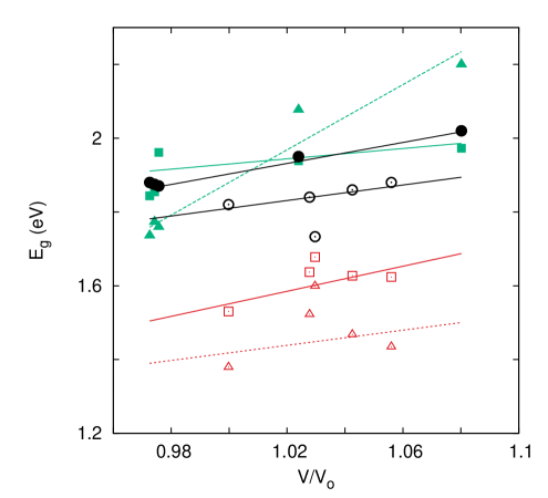
Considering that the variation in lattice parameters would result in residual stress effects that would manifest as pressure, we expect changes in conduction band, valence band shapes and band gaps [10, 19]. Georgies et al [10], Makinistian et al [19] and Parenteau et al [21] works show that the band gap of SnS is directly proportional to the unit cell’s volume, with band gap approaching small values as volume decreases. Fig 8 show the results of our calculations for samples grown on ITO and glass respectively for different thicknesses. The linearity is in confirmation of results in literature and experimental results highlighted in fig (6) and fig (8). The theoretical work hence matches and substantiates the experimental results. However, the theoretical calculations of band structure does not take into account grain boundary and hence is not in a position to comment on the variation of band gap with grain size. As stated in our section on experimental results, the band gap depends on both the grain size and lattice’s unit cell volume (via lattice parameter). To this extent, we believe that the two variables are acting independent of each other and are hence separable. Eqn (5) should then be written as
| (6) | |||||
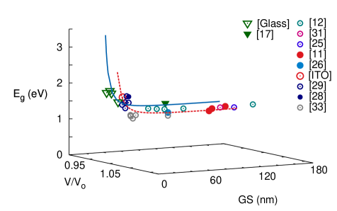
Fig (9) shows a three dimensional plot of our experimental data along with data collected from various literature [11, 12],[28]-[35] on SnS thin films. It is seen that the data points arrange themselves along two family of graphs, namely on 0.975 and 0.995 for various grain sizes. A large volume of data exists for . Again if we consider eqn (5) to be valid, then a family of curves should not have existed. If forced to curve fit, then identical values of and should returnned. This is not the case. A look into the derivation of Brus [16] eqn (5) would show that it considers the electron’s Coulombic interactions only. This interaction become prominant only when the electrons are confined in grains whose dimension are on the nano-scale. In large crystals, these interactions are neglected since the electrons are far apart and their interactions are only with the lattice potential whose periodicity is related to the lattice parameter. The curvature of the band structures thus formed due to the electron lattice potential interaction, is related to the magnitude of the effective mass. Our results suggest, that even at the nano-scale, the electron lattice potential interaction can not be neglected and has to be considered along with the electron-electron interaction potential. Results emerging from fig (9) suggest that resulting Schrodinger equation is solvable by separable variable method leading to an expression like eqn (6).
Correcting for the lattice parameter, we have reduced effective mass for () 0.975 and 0.995 as and , respectively. This is more near to the values given in literature by theoretical calculations [5, 9, 10] and confirmed by our own theoretical calculations. The data points on the two set of curves of fig (9) are from various sources and include those on glass and ITO substrates. Hence, the trend now is fully explained by grain size and lattice parameter.
5 Conclusions
The variation in experimental data of SnS thin nano-crystalline film’s band gap in the present work and of those from the literature are completely explained by considering it to be a two variable problem. The band gap depends on the grain size and the lattice volume through the lattice parameters. Theoretical calculations have been used where ever possible to corroborate the results. The results are of significance in Material Science where material characteristics are manipulated as per requirement.
Acknowledgement
Discussions with Sukanta Dutta, Department of Physics, S.G.T.B. Khalsa College is gratefully acknowledged. One of the authors (YG) would like to acknowledge DST (India) for the fellowship (Fellowship No. IF131164) awarded under its Inspire Scheme. The authors (AAN, MVW and EAA), acknowledge the financial support from the Universidad Nacional de Entre Ríos (UNER) and the Consejo Nacional de Investigaciones Científicas y Tecnicas (CONICET), Argentina.
References
References
- [1] C. Gao, H. Shen, Z. Shen, Mater. Lett., 65 (2011) 1413.
- [2] G.H. Yue, D.L. Peng, P.X. Yan, L.S. Wang, W. Wang, X.H. Luo, J Alloy Compd., 468 (2009) 254.
- [3] O.E. Ogah, K. Ramakrishna Reddy, G. Zoppi, I. Forbes, R.W. Miles, Thin Solid Films 519 (2011) 7425.
- [4] M. Leach, K.T. Ramakrishna Reddy, M.V. Reddy, J.K. Tan, D.Y. Jang and R.W. Miles, Energy Procedia 15 (2012) 371.
- [5] W. Albers, C. Haas, H.J. Vink, and J.D. Wasscher, J Appl. Phys., 2 (1961) 2220.
- [6] P. Sinsermsuksakul, J. Heo, W. Noh, A.S. Hock, and R.G. Gordon, Adv Energy Mater, 1 (2011) 1116.
- [7] L. Makinistian, E. A. Albanesi, Phys. Status Solidi B, 246 (2009) 183.
- [8] E.D. Cullity and S.R. Stock, “Elements of X-Ray Diffraction”, 3rd Ed., Prentice-Hall Inc (NJ, 2001).
- [9] J. Vidal, S. Lany, M. d’Avezac, A. Zunger, A. Zakutayev, J. Franeis, J Tate, Appl. Phys. Lett., 100 (2012) 032104.
- [10] G.A. Tritsaris, B.D. Malone and E. Kaxiras, J App Phys 113 (2013) 233507.
- [11] M. Devika, N.K. Reddy, D.S. Reddy, S.V. Reddy, K. Ramesh, E.S.R. Gopal, K.R. Gunasekhar, V. Ganesan and Y.B. Hahn, J. Phys.: Condens. Matter, 19 (2007) 306003.
- [12] M. Devika, N.K. Reddy, K. Ramesh, H.R. Sumana, K.R. Gunasekhar, E.S.R. Gopal and K.T. Ramakrishna Reddy, Semicond. Sci. Tech., 21 (2006) 1495.
- [13] J. Tauc, Mat. Res. Bull., 5 (1970) 721.
- [14] M. Ristov, G.Sinadinovski, J. Grozdanov, M.Mitreski, Thin Solid Films, 173 (1989) 53.
- [15] P.Tyagi, A.G.Vedeshwar, Phys. Rev. B, 63 (2001) 245315.
- [16] L.E. Brus, J. Chem. Phys. 80 (1984) 094403.
- [17] B. Ghosh, M. Das, P. Banerjee, S. Das, Semicond. Sci. Tech., 23 (2008) 125013.
- [18] L. Ehm, K. Knorr, P. Dera, A. Krimmel, P. Bouvier, M. Mezouar, J. Phys: Condens. Matter., 16 (2004) 3545.
- [19] L. Makinistian, E.A. Albanesi, Comp. Mater. Sci., 50 (2011) 2872.
- [20] P. Blaha, K. Schwarz, J. Luitz, Viena University of Technology, 2001. Improved and updated version of the WIEN code, published by P. Blaha, K. Schwarz, P. Sorantin, S.B. Rickey, Comput. Phys. Commun. 59 (1990) 399.
- [21] M. Parenteau and C. Carlone, Phys Rev B, 41 (1990) 5227.
- [22] M. Calixtro-Rodriguez, H. Martinez, A. Sanchez-Juarez, J. Campos-Alvarez, A. Tiburcio-Silver, M.E. Calixto, Thin Solid Films 517 (2009) 2497.
- [23] X. Gou, J. Chen, P. Shen, Mater. Chem. Phys. 93 (2005) 557.
- [24] P. Jain, P. Arun, Thin Solid Films 548 (2013) 241.
- [25] L. Hedin, S. Lundqvist, Solid State Phys. 23 (1970) 1.
- [26] L. Hedin, Phys. Rev. 139 (1965) A796.
- [27] L. Makinistian, E.A. Albanesi, Comp. Mater. Sci., 50 (2011) 2872.
- [28] M. Devika, K.T.Ramakrishna, N.K. Reddy, K.Ramesh, R. Ganesan, E.S.R. Gopal, K.R. Gunasekhar, J. Appl. Phys., 100 (2006) 023518.
- [29] E. Turan, M. Kul, A.S. Abyek, M. Zor, J. Phys. D. Appl. Phys., 42 (2009) 245408.
- [30] Y. Aziyan-Kalandaragh, A. Khodayari, Z. Zeng, C.S. Garoufalis, S. Baskoutas, L.C.Gontard, J. Nanopart. Res., 15 (2013) 1388.
- [31] T.H. Patel, Open Surf. Sci. J, 4 (2012) 6.
- [32] A. Gomez, H. Martinez, M. Calixto-Rodriguez, D. Avellaneda, P.G. Reyes, O. Flores, J Mater. Sci. Eng. B, 3 (2013) 352.
- [33] T.H. Sajessh, A.R. Warrier, C.S. Kartha, K.P. Vijayakumar, Thin Solid Films, 518 (2010) 4370.
- [34] M. Devika, N.K. Reddy, K. Ramesh, K.R. Gunasekhar, E.S.R. Gopal, K.T.R. Reddy, Semicond. Sci. Tech., 21 (2006) 1125.
- [35] S. Chen, Y. Chen, Y. He, G. Chen, Mater Lett 61 (2007) 1408.