Electronic Structures of Hybrid Graphene/Phosphorene Nanocomposite
Abstract
Combining the electronic structures of two-dimensional monolayers in ultrathin hybrid nanocomposites is expected to display new properties beyond their simplex components. Here, first-principles calculations are performed to study the structural, electronic and optical properties of hybrid graphene and phosphorene nanocomposite. It turns out that weak van der Waals interactions dominate between graphene and phosphorene with their intrinsic electronic properties preserved. Hybrid graphene and phosphorene nanocomposite shows tunable band gaps at graphene’s Dirac point and a transition from hole doing to electron doing for graphene as the interfacial distance decreases. Charge transfer between graphene to phosphorene induces interfacial electron-hole pairs in hybrid graphene and phosphorene nanocomposite with enhanced visible light response.
pacs:
I Introduction
Two-dimensional (2D) ultrathin materials, such as graphene,Scinece_306_666_2004 ; NatureMater_6_183_2007 silicene,PRL_102_236804_2009 ; SSR_67_1_2012 hexagonal boron nitride,NatureMater_3_404_2004 ; NanoLett_10_3209_2010 graphitic carbon nitride,NatureMater_8_76_2009 ; JPCL_3_3330_2012 graphitic zinc oxide,JMC_15_139_2005 ; PRL_96_066102_2006 molybdenum disulphide,PRL_105_136805_2010 ; NatureNanotechnol_6_147_2011 have received considerable interest recently owing to their outstanding properties and potential applications. Graphene,NatureMater_6_183_2007 a 2D sp2-hybridized carbon monolayer, is known to have remarkable electronic properties, such as a high carrier mobility, but the absence of a bandgap limits its applications of large-off current and high on-off ratio for graphene-based electronic devices. Furthermore, intrinsic electronic properties of graphene depend sensitively on the substrates due to strong graphene-substrate interactions, such as SiO2,NatPhys_4_144_2008 ; PRL_106_106801_2011 SiCNatureMater_6_770_2007 ; PRL_108_246104_2012 and metalPRL_101_026803_2008 ; NatureNanotech_6_179_2011 surfaces. Therefore, opening a small bandgap and finding an ideal substrate for graphene remains challenging in the experiments.
Interestingly, many 2D ultrathin hybrid graphene-based nanocomposites have been widely studied experimentally and theoretically, such as graphene/silicene (G/S),JCP_139_154704_2013 ; PRB_88_245408_2013 ; APL_103_261904_2013 graphene/graphitic boron nitride (G/g-BN),Nature_5_722_2010 ; NatureMater_10_282_2011 ; PRB_81_155433_2010 graphene/graphitic carbon nitride (G/g-C3N4),JPCC_115_7355_2011 ; JACS_133_8074_2011 ; JACS_134_4393_2012 , graphene/graphitic zinc oxide (G/g-ZnO)JCP_138_124706_2013 ; JPCC_117_10536_2013 ; JAP_113_054307_2013 and graphene/molybdenum disulphide (G/MoS2)Nanoscale_3_3883_2011 ; JPCC_117_15347_2013 ; Science_340_1311_2013 These hybrid graphene-based nanocomposites show much more new properties far beyond their simplex components. Furthermore, most of them are ideal substrates for graphene to preserve the intrinsic electronic properties of graphene and substrates.
Most recently, a new 2D material, namely, black phosphorus monolayer or phosphorene,PRB_86_035105_2012 ; JPCC_118_14051_2014 ; NatureNanotech_9_372_2014 ; NatureCommun_5_4475_2014 has been isolated in the experiments through mechanical exfoliation from bulk black phosphorus and has immediately received considerable attention. Phosphorene also shows some remarkable electronic properties superior to graphene. For example, phosphorene is a semiconductor with a direct bandgap of about 1 ,JPCC_118_14051_2014 showing the drain current modulation up to 105 and carrier mobility up to 103 cm2/(Vs) in nanoelectronics.NatureNanotech_9_372_2014 Here, an interesting question arise: whether graphene and phosphorene can form a 2D hybrid G/P nanocomposite with new properties?
In the present work, we design a new 2D hybrid graphene and phosphorene nanocomposite and study its electronic and optical properties with first-principles calculations. The results show that graphene interacts overall weakly with phosphorene via van der Waals (vdW) interactions, thus, their intrinsic electronic properties can be preserved in hybrid graphene/phosphorene nanocomposite. Moreover, interlayer interactions in hybrid graphene/phosphorene nanocomposite can induce tunable band gaps at graphene’s Dirac point, a transition from hole doing to electron doing for graphene and enhanced visible light response.
II Theoretical Methods and Models
The lattice parameters of graphene and phosphorene calculated to setup unit cell are (G) = (G) = 2.47 Å,JCP_139_154704_2013 (P) = 4.62 Å and (P) = 3.30 Å.JPCC_118_14051_2014 We design a new 2D hybrid graphene/phosphorene nanocomposite (40 carbon atoms and 28 phosphorus atoms) as shown in Figure 1 with a small lattice mismatch less than 2%. The vacuum space in the Z direction is about 15 Å to separate the interactions between neighboring slabs.
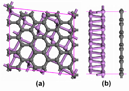
First-principles calculations are based on the density functional theory (DFT) implemented in the VASP package.PRB_47_558_1993_VASP The generalized gradient approximation of Perdew, Burke, and Ernzerhof (GGA-PBE)PRL_77_1996 with van der Waals (vdW) correction proposed by Grimme (DFT-D2)JCC_27_1787_2006_Grimme is chosen due to its good description of long-range vdW interactions.JPCC_111_11199_2007 ; PCCP_10_2722_2008 ; NanoLett_11_5274_2011 ; PRB_83_245429_2011 ; PRB_85_125415_2012 ; PRB_85_235448_2012 ; JPCL_4_2158_2013 ; PCCP_15_5753_2013 ; Nanoscale_5_9062_2013 As an benchmark, DFT-D2 calculations give a good bilayer distance of = 3.25 and binding energy of Eb = -25 per carbon atom for bilayer graphene, which fully agree with previous experimentalPR_100_544_1955 ; PRB_69_155406_2004 and theoreticalPRB_85_205402_2012 ; JCP_138_054701_2013 studies. The energy cutoff is set to be 500 . The surface Brillouin zone is sampled with a 3 3 regular mesh and 120 points are used for calculating the tiny band gaps at the Dirac point graphene in the hybrid G/P nanocomposite supercell. All the geometry structures are fully relaxed until energy and forces are converged to 10-5 and 0.01 /Å, respectively.
To investigate the optical properties of hybrid G/P nanocomposite, the frequency-dependent dielectric matrix is calculated.PRB_73_045112_2006 In order to calculate the optical properties of hybrid G/P nanocomposite, a large 6 6 regular mesh for the surface Brillouin zone, a large number of empty conduction band states (two times more than the number of valence band) and frequency grid points (2000) are adopted. We crosscheck the optical properties of graphene and phosphorene, consistent with previous theoretical calculations.JCP_139_154704_2013 ; NatureCommun_5_4475_2014
III Results and Discussion
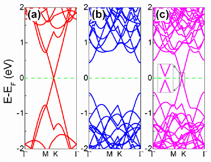
Electronic properties of pristine graphene and phosphorene monolayers in the supercells are checked first and their electronic band structures are plotted in Figure 2a and 2b. Graphene is a zero-gap semiconductor (Figure 2a), showing a linear Dirac-like dispersion relation () = around the Fermi level where F is the Fermi velocity, and F = 0.8106 at the Dirac point of graphene. Monolayer phosphorene is semiconducting with a direct band gap of 0.85 (Figure 2b), which agrees well with previous theoretical studies.JPCC_118_14051_2014
We then study the geometric structures of hybrid G/P nanocomposite. Typical vdW equilibrium spacing of about 3.43 Å with corresponding small binding energy of about -24.7 per atom of graphene is obtained for hybrid G/P nanocomposite, which is well comparable with recent theoretical calculations in 2D graphene based nanocomposites, such as G/S,JCP_139_154704_2013 G/g-BN,PRB_81_155433_2010 G/g-C3N4,JACS_134_4393_2012 G/g-ZnOJCP_138_124706_2013 and G/MoS2.Nanoscale_3_3883_2011 Thus, weak vdW interactions dominate between graphene and phosphorene, suggesting that phosphorene can be used as an ideal substrate for graphene with their intrinsic electronic structures undisturbed. Notice that the small lattice mismatch of about 2% for graphene and phosphorene has little effect on their electronic properties in hybrid G/P nanocomposite.
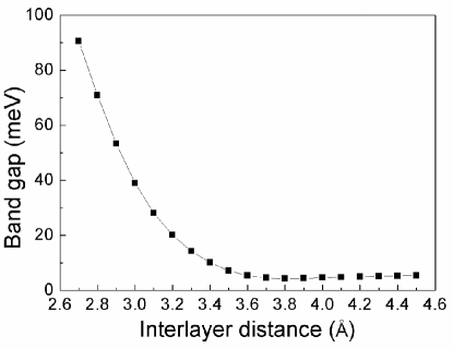
Electronic band structure of hybrid G/P nanocomposite is shown in Figure 2c. The Dirac point of graphene is still preserved, and the Fermi velocity at the Dirac point is almost unchanged (F = 0.8106 ) in hybrid G/P nanocomposite compared to free-standing graphene, though small band gap of 10 is opened at the Dirac point of grpahene. Notice that induced band gaps at the Dirac point of graphene are typically sensitive and tunable to other external conditions, such as interlayer separation,JCP_139_154704_2013 as plotted in Figure 3. The gap values at graphene’s Dirac point increase from 5 to 90 as the interfacial distance decreases from 3.7 to 2.7 Å in hybrid G/P nanocomposite, showing a potential for high-performance graphene-based electronic devices.
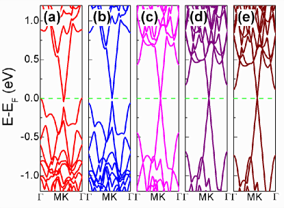
Interestingly, we find that the Dirac point of graphene moves form the conduction band to the valence band of phosphorene as the interfacial distance decreases from 4.5 to 2.7 Å in hybrid G/P nanocomposite, inducing a transition from hole (p-type) doping to electron (n-type) doping for graphene as shown in Figure 4. When the interfacial distance artificially increases larger than 4.5 Å, graphene’s Dirac point is close to phosphorene’s conduction band. That is because graphene’s work function (4.3 ) is close to phosphorene’s nucleophilic potential (4.1 ). Based on the Schottky-Mott model,PR_71_717_1947 electrons easily transfer from graphene to phosphorene, resulting in p-type doping of graphene. But, weak overlap of electronic states between graphene and phosphorene are enhanced as the interfacial distance decreases. Furthermore, carbon has a large electronegativity (2.55) than that (2.19) of phosphorus. Thus, when graphene and phosphorene are close to each other (smaller than 3.0 Å), electrons easily transferred from phosphorene to graphene, resulting in n-type doping of graphene. Similarly, interlayer-interaction induced a transition from p-type doping to n-type doping for graphene has also observed experimentally and theoretically in hybrid graphene/silicene nanocompositeJCP_139_154704_2013 and graphene adsorption on some metal substrates.PRL_101_026803_2008
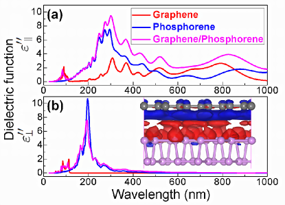
Besides commonly focused electronic structures in 2D graphene based nanocomposites, we also study the optical properties in hybrid G/P nanocomposite. Though pristine graphene and phosphorene themselves display unique optical properties,JCP_139_154704_2013 ; NatureCommun_5_4475_2014 interlayer interactions and charge transfer in 2D nanocomposites may induce new optical transitions.JPCL_3_3330_2012 ; JCP_138_124706_2013 As shown in Figure 5, charge transfer between graphene to phosphorene induces interfacial electron-hole pairs in hybrid G/P nanocomposite. In optical property calculations, the imaginary part of dielectric function for graphene and phosphorene monolayers as well as corresponding hybrid G/P nanocomposite are evaluated, including the light polarized parallel and perpendicular to the plane, as shown in Figure 5. Parallel optical absorption of pristine graphene and phosphorene monolayers mainly possesses in the visible light range from 200 to 1000 due to the transitions from to ∗ states and to ∗ states. Hybrid G/P nanocomposite exhibits stronger optical absorption, especially in the visible light range from 300 to 800 , compared with simplex graphene and phosphorene monolayers, because the interlayer coupling in hybrid G/P nanocomposite induces electronic states overlap and electrons can now be directly excited between graphene and phosphorene. But, perpendicular dielectric function is almost unaffected by the interlayer interactions in hybrid G/P nanocomposite due to very weak optical absorption of graphene in this direction.
IV Conclusions
In summary, we study the electronic structures and optical properties of hybrid graphene/phosphorene nanocomposite with first-principles calculations. We find that phosphorene interacts weakly with graphene via weak vdW interactions to preserve their intrinsic electronic properties. Moreover, interlayer interactions can induce tunable band gaps at graphene’s Dirac point, a transition from hole doing to electron doing for graphene and enhanced visible light response in hybrid graphene/phosphorene nanocomposite. With the excellent electronic and optical properties combined beyond simplex graphene and phosphorene monolayers, 2D ultrathin hybrid graphene/phosphorene nanocomposite system is expected to be of a great potential in new graphene-based electronic devices.
V ACKNOWLEDGMENTS
This work is partially supported by the National Key Basic Research Program (2011CB921404), by NSFC (11404109, 21121003, 91021004, 21233007, 21222304), by CAS (XDB01020300). This work is also partially supported by the Scientific Discovery through Advanced Computing (SciDAC) program funded by U.S. Department of Energy, Office of Science, Advanced Scientific Computing Research and Basic Energy Sciences (W. H.). We thank the National Energy Research Scientific Computing (NERSC) center, USTCSCC, SC-CAS, Tianjin, and Shanghai Supercomputer Centers for the computational resources.
References
- (1) K. S. Novoselov, A. K. Geim, S. V. Morozov, D. Jiang, Y. Zhang, S. V. Dubonos, I. V. Grigorieva, and A. A. Firsov, Scinece 306, 666 (2004).
- (2) A. K. Geim and K. S. Novoselov, Nature Mater. 6, 183 (2007).
- (3) S. Cahangirov, M. Topsakal, E. Aktürk, H. Şahin, and S. Ciraci, Phys. Rev. Lett. 102, 236804 (2009).
- (4) A. Kara, H. Enriquez, A. P. Seitsonend, L. C. L. Y. Voone, S. Vizzini, B. Aufrayg, and H. Oughaddoub, Surf. Sci. Rep. 67, 1 (2012).
- (5) K. Watanabe, T. Taniguchi and H. Kanda, Nature Mater. 3, 404 (2004).
- (6) L. Song, L. Ci, H. Lu, P. B. Sorokin, C. Jin, J. Ni, A. G. Kvashnin, D. G. Kvashnin, J. Lou, B. I. Yakobson and P. M. Ajayan, Nano Lett. 10, 3209 (2010).
- (7) X. Wang, K. Maeda, A. Thomas, K. Takanabe, G. Xin, J. M. Carlsson, K. Domen and M. Antonietti, Nature Mater. 8, 76 (2009).
- (8) F. Wu, Y. Liu, G. Yu, D. Shen, Y. Wang, and E. Kan, J. Phys. Chem. Lett. 3, 3330 (2012).
- (9) F. Claeyssens, C. L. Freeman, N. L. Allan, Y. Sun, M. N. R. Ashfold, and J. H. Harding, J. Mater. Chem. 15, 139 (2005).
- (10) C. L. Freeman, F. Claeyssens, and N. L. Allan, Phys. Rev. Lett. 96, 066102 (2006).
- (11) K. F. Mak, C. Lee, J. Hone, J. Shan, and T. F. Heinz, Phys. Rev. Lett. 105, 136805 (2010).
- (12) B. Radisavljevic, A. Radenovic, J. Brivio, V. Giacometti, and A. Kis, Nature Nanotech. 6, 147 (2011).
- (13) J. Martin, N. Akerman, G. Ulbricht, T. Lohmann, J. H. Smet, K. von Klitzing, and A. Yacoby, Nature Phys. 4, 144 (2008).
- (14) N. T. Cuong, M. Otani, and S. Okada, Phys. Rev. Lett. 106, 106801 (2011).
- (15) S. Y. Zhou, G.-H. Gweon, A. V. Fedorov, P. N. First, W. A. de Heer, D.-H. Lee, F. Guinea, A. H. C. Neto, and A. Lanzara, Nature Mater. 6, 770 (2007).
- (16) J. Ristein, S. Mammadov, and T. Seyller, Phys. Rev. Lett. 108, 246104 (2012).
- (17) G. Giovannetti, P. A. Khomyakov, G. Brocks, V. M. Karpan, J. van den Brink, and P. J. Kelly, Phys. Rev. Lett. 101, 026803 (2008).
- (18) F. Xia, V. Perebeinos, Y. Lin, Y. Wu, and P. Avouris, Nature Nanotech. 6, 179 (2011).
- (19) W. Hu, Z. Li, and J. Yang, J. Chem. Phys. 139, 154704 (2013).
- (20) Y. Cai, C.-P. Chuu, C. M. Wei, and M. Y. Chou, Phys. Rev. B 88, 245408 (2013).
- (21) M. Neek-Amal, A. Sadeghi, G. R. Berdiyorov and F. M. Peeters, Appl. Phys. Lett. 103, 261904 (2013).
- (22) C. R. Dean, A. F. Young, I. Meric, C. Lee, L. Wang, S. Sorgenfrei, K. Watanabe, T. Taniguchi, P. Kim, K. L. Shepard, and J. Hone, Nature Nanotech. 5, 722 (2010).
- (23) J. Xue, J. Sanchez-Yamagishi, D. Bulmash, P. Jacquod, A. Deshpande, K. Watanabe, T. Taniguchi, P. Jarillo-Herrero, and B. LeRoy, Nature Mater. 10, 282 (2011).
- (24) J. Sławińska, I. Zasada, and Z. Klusek, Phys. Rev. B 81, 155433 (2010).
- (25) Q. J. Xiang, J. G. Yu, and M. Jaroniec, J. Phys. Chem. C 115, 7355 (2011).
- (26) X.-H. Li, J.-S. Chen, X. Wang, J. Sun, and M. Antonietti, J. Am. Chem. Soc. 133, 8074 (2011).
- (27) A. Du, S. Sanvito, Z. Li, D. Wang, Y. Jiao, T. Liao, Q. Sun, Y. H. Ng, Z. Zhu, R. Amal, and S. C. Smith, J. Am. Chem. Soc. 134, 4393 (2012).
- (28) W. Hu, Z. Li, and J. Yang, J. Chem. Phys. 138, 124706 (2013).
- (29) W. Geng, X. Zhao, H. Liu, and X. Yao, J. Phys. Chem. C 117, 10536 (2013).
- (30) X. Guo and Y. G. Zhou, J. Appl. Phys. 113, 054307 (2013).
- (31) Y. Ma, Y. Dai, M. Guo, C. Niu, and B. Huang, Nanoscale 3, 3883 (2011).
- (32) X. D. Li, S. Yu, S. Q. Wu, Y. H. Wen, S. Zhou, and Z. Z. Zhu, J. Phys. Chem. C 117, 15347 (2013).
- (33) L. Britnell, R. M. Ribeiro, A. Eckmann, R. Jalil, B. D. Belle, A. Mishchenko, Y.-J. Kim, R. V. Gorbachev, T. Georgiou, S. V. Morozov, A. N. Grigorenko, A. K. Geim, C. Casiraghi, A. H. C. Neto, K. S. Novoselov, Science 340, 1311 (2013).
- (34) S. Appalakondaiah, G. Vaitheeswaran, S. Leb gue, N. E. Christensen, and A. Svane, Phys. Rev. B 86, 035105 (2012).
- (35) H. Guo, N. Lu, J. Dai, X. Wu, and X. C. Zeng, J. Phys. Chem. C 118, 14051 (2014).
- (36) L. Li, Y. Yu, G. Ye, Q. Ge, X. Ou, H. Wu, D. Feng, X. Chen, and Y. Zhang, Nature Nanotech. 9, 372 (2014).
- (37) J. Qiao, X. Kong, Z.-X. Hu, F. Yang, and W. Ji, Nature Commun. 5, 4475 (2014).
- (38) G. Kresse and J. Hafner, Phys. Rev. B 47, 558 (1993).
- (39) J. P. Perdew, K. Burke, and M. Ernzerhof, Phys. Rev. Lett. 77, 3865 (1996).
- (40) S. Grimme, J. Comput. Chem. 27, 1787 (2006).
- (41) S. Grimme, C. Muck-Lichtenfeld, and J. Antony, J. Phys. Chem. C 111, 11199 (2007).
- (42) J. Antony and S. Grimme, Phys. Chem. Chem. Phys. 10, 2722 (2008).
- (43) N. Kharche and S. K. Nayak, Nano Lett. 11, 5274 (2011).
- (44) J. Sławińska, P. Dabrowski, and I. Zasada, Phys. Rev. B 83, 245429 (2011)
- (45) R. Kagimura, M. S. C. Mazzoni, and H. Chacham, Phys. Rev. B 85, 125415 (2012).
- (46) Y. Ma, Y. Dai, M. Guo, and B. Huang, Phys. Rev. B 85, 235448 (2012).
- (47) L. Chen, L. Wang, Z. Shuai, and D. Beljonne, J. Phys. Chem. Lett. 4, 2158 (2013).
- (48) W. Hu, X. Wu, Z. Li, and J. Yang, Phys. Chem. Chem. Phys. 15, 5753 (2013).
- (49) W. Hu, X. Wu, Z. Li and J. Yang, Nanoscale 5, 9062 (2013).
- (50) Y. Baskin and L. Mayer, Phys. Rev. 100, 544 (1955).
- (51) R. Zacharia, H. Ulbricht, and T. Hertel, Phys. Rev. B 69, 155406 (2004).
- (52) R. E. Mapasha, A. M. Ukpong, and N. Chetty, Phys. Rev. B 85, 205402 (2012).
- (53) W. Hu, Z. Li, and J. Yang, J. Chem. Phys. 138, 054701 (2013).
- (54) M. Gajdos̆, K. Hummer, and G. Kresse, Phys. Rev. B 73, 045112 (2006).
- (55) J. Bardeen, Phys. Rev. 71, 717 (1947).