Dielectric Metasurfaces for Complete Control of Phase and Polarization with Subwavelength Spatial Resolution and High Transmission
Metasurfaces are planar structures that locally modify the polarization, phase, and amplitude of light in reflection or transmission, thus enabling lithographically patterned flat optical components with functionalities controlled by design Kildishev2013a ; Yu2014 . Transmissive metasurfaces are especially important, as most optical systems used in practice operate in transmission. Several types of transmissive metasurfaces have been realized Yu2011 ; Lin2014a ; Lin2013 ; Vo2014 , but with either low transmission efficiencies or limited control over polarization and phase. Here we show a metasurface platform based on high-contrast dielectric elliptical nano-posts which provides complete control of polarization and phase with sub-wavelength spatial resolution and experimentally measured efficiency ranging from 72% to 97%, depending on the exact design. Such complete control enables the realization of most free-space transmissive optical elements such as lenses, phase-plates, wave-plates, polarizers, beam-splitters, as well as polarization switchable phase holograms and arbitrary vector beam generators using the same metamaterial platform.
Polarization, phase, and amplitude completely characterize monochromatic light. In free space optical systems, polarization is modified using wave retarders, polarizers, and polarization beam splitters, phase is shaped using lenses, curved mirrors or spatial phase modulators, and amplitude is controlled via neutral density absorptive or reflective filters. Several metasurface platforms have been recently investigated to replicate the functionality of common optical components such as wave retarders, polarizers, beam splitters, lenses, or focusing mirrors. However, none of the platforms achieves complete control of both polarization and phase with sub-wavelength sampling and high transmission. A metasurface platform achieves complete control over polarization and phase if it can generate any desired physically admissible spatially varying polarization and phase distributions from an input beam with arbitrary polarization and phase distributions. Plasmonic metasurfaces have been demonstrated, but they have limited efficiencies because of fundamental limits Monticone2013 ; Arbabi2014b and metal absorption loss Aieta2012 ; Pfeiffer2013 ; Lin2013 . Components based on 1D high contrast gratings have higher efficiencies, but do not provide high spatial resolution for realizing precise phase or polarization profiles in the direction along the grating lines Fattal2010 ; Lu2010 ; Klemm2013 ; Lin2014a ; Aieta2015 . The majority of flat elements have been realized using a platform that provides only phase control Warren1995 ; Lalanne1999 ; Fattal2010 ; Yu2011 ; Klemm2013 ; Lin2014a ; Vo2014 ; Arbabi2014 ; Arbabi2015 ; Vo2014 ; West2014 ; Decker2015 (in most cases only for a fixed input polarization), or only a limited polarization modification capability Kikuta1997 ; Lin2013 ; Schonbrun2011 ; Yang2014 ; Mutlu2012c ; Zhao2012 . The platform we propose does not suffer from these limitations and provides a unified framework for realizing any device for polarization and phase control with an average transmission higher than 85%.
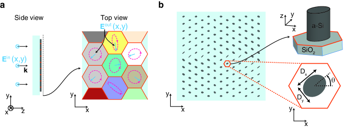
A generic illustration of a transmissive metasurface which provides spatially varying control of phase and polarization for monochromatic light is shown in Fig. 1a. In this illustration, the metasurface is divided into hexagonal pixels, but other lattice types could also be chosen. An optical wave with spatially varying electric field is incident on the metasurface. The polarization ellipse and the phase of the optical field transmitted through each pixel can be controlled arbitrarily via the pixel design (Fig. 1a, top view). To avoid diffraction of light into non-zero diffraction orders, and to achieve high polarization and phase gradients required for implementation of optical components such as lenses with high numerical apertures, it is important that each pixel has a lateral dimension smaller than a wavelength. The general relation between the electric fields of the input and output waves at each pixel is expressed using the Jones matrix () of the pixel as . It is shown in the Supplementary Section S1 that, for metasurfaces with high transmission, any arbitrary () can be mapped to any desired () using a symmetric and unitary Jones matrix. Therefore, a metasurface platform achieves complete polarization and phase control if it can implement any unitary and symmetric Jones matrix at each pixel.
Figure 1b shows a schematic illustration of the proposed metasurface platform. It is composed of a single layer array of amorphous silicon elliptical posts with different sizes and orientations, resting on a fused silica substrate. The posts are placed at the centres of hexagonal unit cells. In a simplified picture, each post can be considered a waveguide which is truncated on both sides and operates as a low quality factor Fabry-Pérot resonator. The elliptical cross section of the waveguide leads to different effective refractive indices of the waveguide modes polarized along the two ellipse diameters. As a result, each of the posts imposes a polarization dependent phase shift to the transmitted light and modifies both its phase and polarization. In the regime of operation considered here (also discussed previously in Arbabi2015 ) light is mainly confined inside the high refractive index posts which behave as weakly coupled low quality factor resonators. Therefore, the light scattered by each post is primarily affected by the geometrical parameters of the post and has negligible dependence on the dimensions and orientations of its neighbouring posts. As a result, each unit cell of the lattice can be considered as a pixel similar to the illustration shown in Fig. 1a.
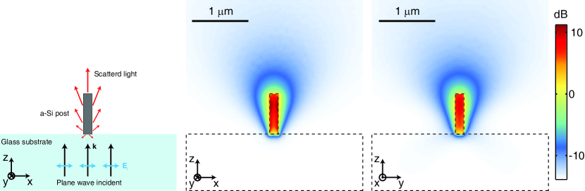
Light scattering by high refractive index single dielectric scatterers has been studied previously, and it has been shown that they may possess strong effective magnetic dipoles and exhibit large forward scattering Garcia-Etxarri2011 ; Evlyukhin2011 ; Spinelli2012 (see Supplementary Fig. 1). Here, instead of studying the properties of a single elliptical post, we use a different approach and examine the transmission properties of periodic arrays of weakly coupled posts. Such periodic arrays better approximate the local transmission properties of a metasurface composed of gradually varying posts. We use the Jones matrix of the periodic arrays to approximate the local Jones matrix of each pixel. This approximation is used here to successfully realize high performance devices for polarization and phase control (discussed later in Fig. 4 and Fig. 5), thus further validating its accuracy.
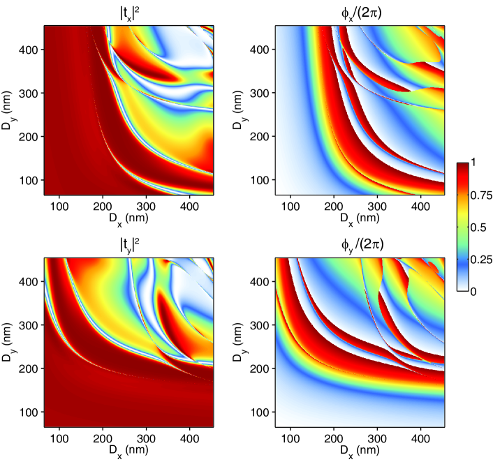
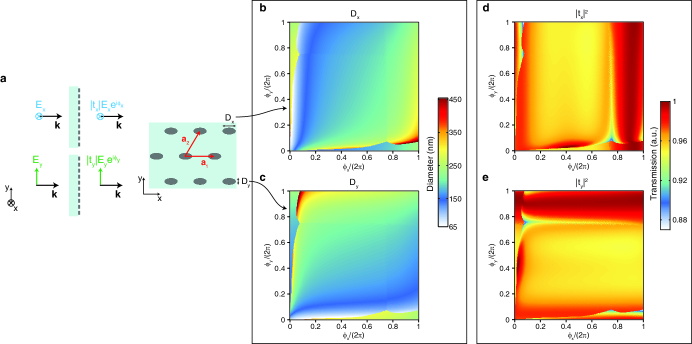
A periodic array of elliptical posts with one ellipse axis aligned to one of the hexagonal lattice vectors ( which is along the axis) is shown in Fig. 2a. Due to symmetry, a normally incident optical wave linearly polarized along one of the ellipse axes does not change polarization and only acquires phase as it passes though the array. The phase shifts imposed by the array to the and -polarized waves (i.e. and ) are functions of the elliptical post diameters and . Therefore, the array behaves as a 2D material with adjustable birefringence whose principal axes are along and directions. The phases ( and ) and the intensity transmission coefficients ( and ) were first determined via simulations as functions of the ellipse diameters (see Methods and Supplementary Figure 2 for details). From these simulations, the required diameters and to achieve all combinations of and while maintaining high transmission were derived, and are plotted in Fig. 2b and 2c. Any combination of and can be simultaneously obtained by properly choosing (from Fig. 2b) and (Fig. 2c). The corresponding intensity transmission coefficients (i.e. and ) are shown in Fig. 2d and 2e, and are larger than 87% for all values of and . The complete phase coverage combined with the high transmission result in the high performance of this platform.
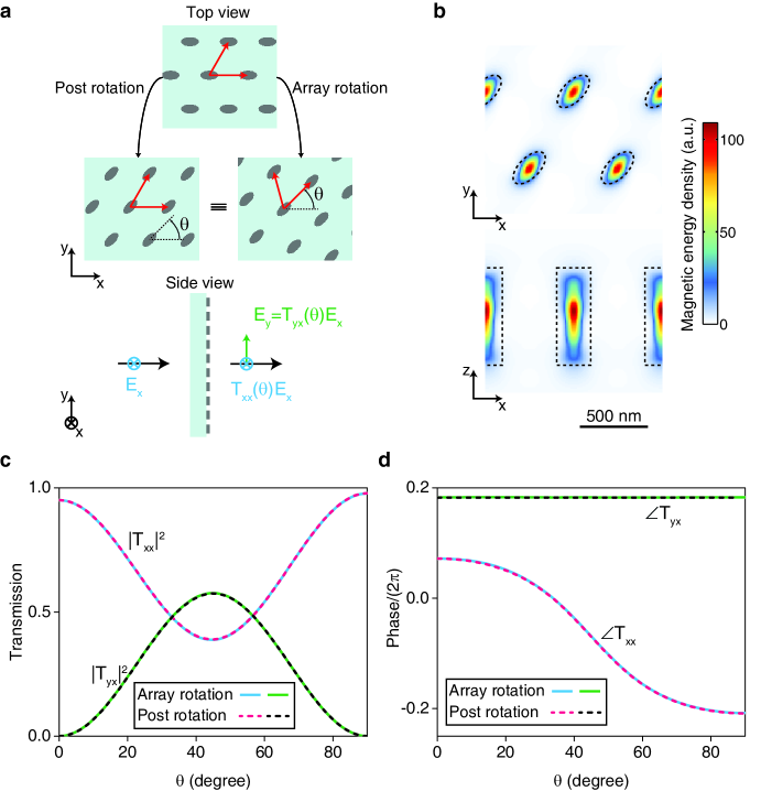
The principal axes of the birefringent array shown in Fig. 2a can be rotated by rotating the entire array or, with good approximation, by rotating all posts around their axes. This can be seen in Fig. 3 which shows that rotating the posts around their axes leads to approximately the same Jones matrix elements as rotating the entire array by the same angle. This is a result of the confinement of the optical energy inside the posts (as can be seen in Fig. 3b) which has led to the weak coupling among the posts Arbabi2015 . This also provides another evidence that the polarization and phase transformation by the elliptical posts can be considered as a local effect.
As we mentioned earlier, a metasurface can achieve complete polarization and phase control if each of its pixels can be designed to realize any unitary and symmetric Jones matrix. It is shown in the Supplementary Section S2 that any desired symmetric and unitary Jones matrix can be realized using a birefringent metasurface if , , and the angle between one of the principal axes of the material and the axis () could be chosen freely. As Figs. 2 and 3 show, all these degrees of freedom are achievable at each pixel through selection of the post diameters and , and its in-plane rotation angle (see the inset of Fig. 1b). Therefore, any desired spatially varying polarization and phase profiles can be generated by sampling the incident wavefront with a sub-wavelength lattice, and placing elliptical posts with proper dimensions and rotation angles at the lattice sites to impart the required phase and polarization change on the transmitted light. The proposed metasurface platform samples both the incident and the transmitted wavefront with sub-wavelength resolution in both silica and air because the reciprocal vectors of the lattice are larger than the wavenumber of light and thus, for close to normal incidence, the first order diffraction is not present.
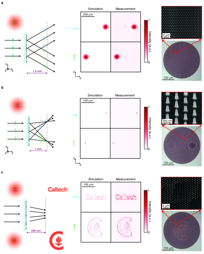
The freedom provided by the proposed platform to simultaneously control the polarization and phase of light allows for implementation of a wide variety of optical components. To demonstrate the versatility and high performance of this platform, we fabricated and characterized two categories of flat optical elements operating at the near infrared wavelength of 915 nm. The devices consist of 715 nm tall amorphous silicon posts with diameters ranging from 65 nm to 455 nm, arranged on a hexagonal lattice with 650 nm lattice constant (for details of fabrication and measurement, see Methods). The first category of devices generate two different wavefronts for two orthogonal input polarizations. This functionality can be achieved if the device does not change the polarization ellipses of the two orthogonal polarizations it has been designed for, and only changes their handedness (see Supplementary Section S3). A special case is when both of the input polarizations are linear. Simulation and experimental measurement results, as well as the optical and scanning electron microscope images of three types of devices in this category are shown in Fig. 4. A polarization beam splitter that deflects and polarized portions of light by 5∘ and -5∘ is presented in Fig. 4a. We measured 72% and 77% efficiencies for the and -polarized input light, respectively. The measured efficiencies are smaller than their corresponding simulated values (89% for and 93% for -polarized incident beams) because of slight differences between the diameters of the designed and fabricated posts. A polarization beam splitter which separates and focuses the and polarized light at two different positions is presented in Fig. 4b. The focusing efficiency (defined as the ratio of the optical power focused to the desired spot to the input power) was measured as 80% and 83% for the and -polarized light, respectively. A polarization switchable phase hologram which generates two distinct patterns for and -polarized light is shown in Fig. 4c. The change of the recorded pattern with polarization is shown in Supplementary Video 1. This is the most general form of device from this category. We measured efficiencies of 84% and 91% for this device for the and -polarized incident light. The measured intensity profiles presented in Fig. 4 show the total transmitted light as detected by the camera and there is no background subtraction.
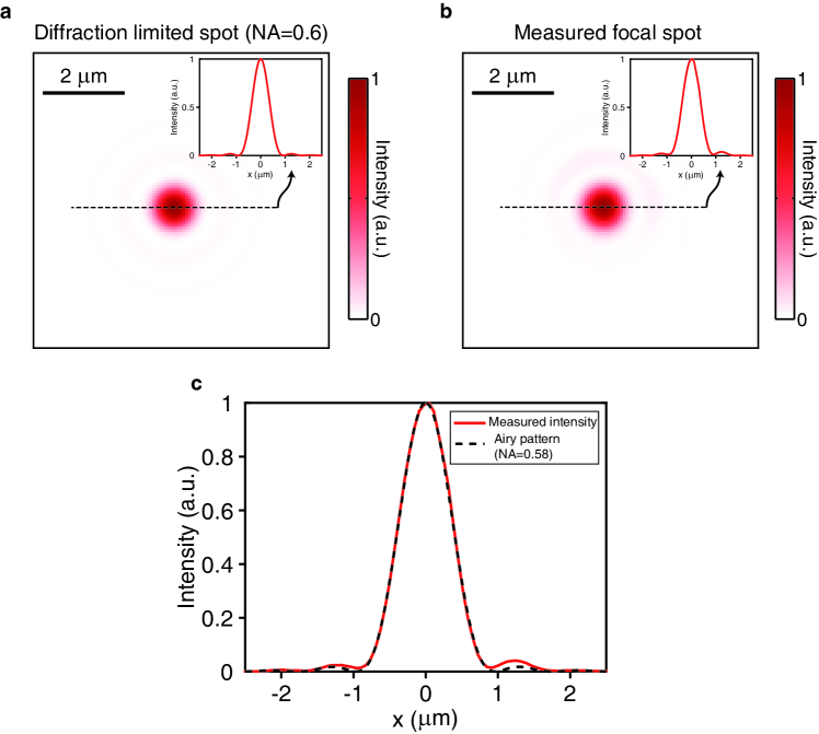
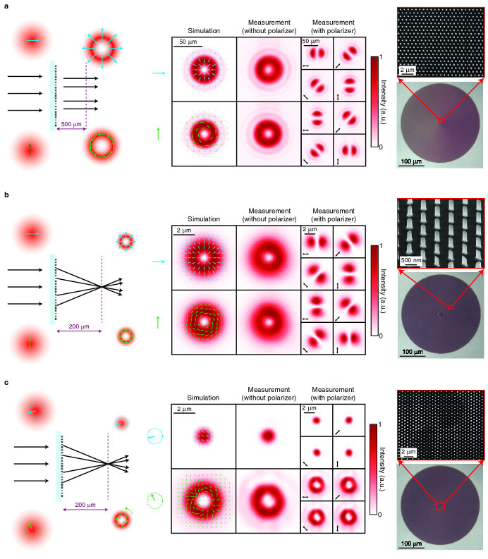
The second category of devices generate light with a desired arbitrary phase and polarization distribution from an incident light with a given polarization. Fig. 5a shows a device that transforms an incident -polarized incident Gaussian beam into a radially polarized Bessel-Gauss beam, and a -polarized incident Gaussian beam into an azimuthally polarized Bessel-Gauss beam. We measured a transmission efficiency of 96% and 97% for the and input polarizations, respectively. Measured intensity profiles for different polarization projections are also shown in Fig. 5. When the polarization of the incident Gaussian beam is linear but not aligned with the or axis, a generalized cylindrical vector beam is generated by this device. It has been recently shown that cylindrical vector beams show unique features such as focus shaping when focused with a high numerical aperture lens Zhan2009 . Furthermore, the same device in Fig. 5a generates light with different orbital angular momentum depending on the helicity of the input beam; right and left handed circularly polarized input beams will respectively acquire and units of orbital angular momentum as they pass through this device. Both the generation and focusing of cylindrical vector beams can be performed using a single device based on the proposed platform. Such a device which simultaneously generates and focuses radially and azimuthally polarized light is shown in Fig. 5b. Similar to the device shown in Fig. 5a, due to the polarization conversion, right and left handed polarized beams acquire plus or minus one units of orbital angular momentum as they pass through the device. As a result, by adding a sinusoidal dependence in the form of to the phase profile of the device, the total orbital angular momentum of the right and left handed circularly polarized light after passing through the device will become and , respectively. A device with such a phase and polarization profile is shown in Fig. 5c. As can be seen from the simulation and measurement results, a right handed circularly polarized incident beam is focused to a nearly diffraction limited spot (see Supplementary Fig. 3) while a left handed circularly polarized beam is focused into a doughnut shaped intensity pattern. Therefore, the focal spot shape can be modified by changing the polarization of the incident beam. This is particularly interesting since the polarization state of the incident beam can be switched rapidly using a phase modulator.
The functionalities provided by some of the optical devices demonstrated here can only be achieved by using a combination of multiple bulk optical components. For example, to realize the functionality of the polarization beam splitter and focuser in Fig. 4b, a Wollaston prism and two carefully aligned lenses are required. The realization of the polarization vector beams shown in Fig. 5 generally requires interferometry Phelan2011 , liquid crystal spatial light modulators, or conical Brewster prisms Kozawa2005 . The complete and simultaneous control over the polarization and phase profiles of light offered by the proposed platform and the design technique enables realization of novel optical components with functionalities exactly tailored to specific applications and with form factors required for emerging applications like wearable consumer electronics. As most other diffractive optical elements, these devices have an optical bandwidth of several percent of the design wavelength Swanson1989 . Thus, they could directly replace conventional optics in applications employing narrow-band light sources such as optical communications, monochromatic imaging and multi-photon microscopy. We note that the theoretical approach and the design technique we introduced here are general and applicable to similar platforms with other types of scatterers and lattice shapes provided they offer complete and independent phase control for two orthogonal polarizations. The operating wavelength can also be changed by scaling the device dimensions. Further improvements are expected from using materials with optical nonlinearities and gain that might extend the spectral bandwidth of operation and provide tunability. These metasurfaces could also be patterned on curved or flexible substrates thus enabling conformal optical devices.
Methods
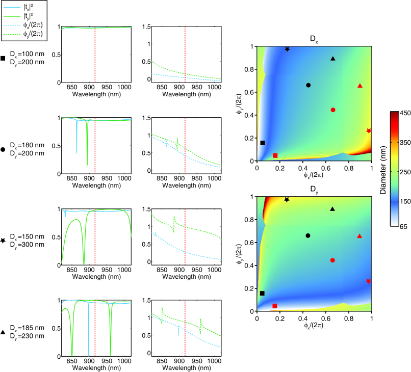
Simulations and design. To obtain the simulation results presented in Figs. 2b and 2c, we computed the transmission coefficients and of and -polarized plane waves for the periodic array shown schematically in Fig. 2a by using the rigorous coupled wave analysis (RCWA) technique using a freely available software package Liu2012 . The simulations were performed at 915 nm. The amorphous silicon posts (with refractive index of 3.56 at 915 nm) are 715 nm tall, and rest on a fused silica substrate. We computed these transmission coefficients for all mutual values of the ellipse diameters and in the range to , where 650 nm is the lattice constant. Simulation results are presented in Supplementary Fig. 2. For normal incidence, the array is non-diffractive in both air and fused silica at wavelengths longer than 816 nm. Next, using the computed transmission coefficients, for all combinations of the phases and we found the diameters and that minimizes the mean squared error . It should be noted that the elliptical posts obtained using this method do not possess resonances close to the operation wavelength since the transmission values go to zero at resonance and increases the mean squared error. Transmission spectra for a few arrays with different diameters are presented in Supplementary Fig. 4.
The simulation results presented in Figs. 3b and 3c were also computed using the RCWA technique. In Fig. 3b, an -polarized light with magnetic energy density of 1 is normally incident on the posts from the top. The simulation parameters used to obtain Figs. 3b and 3c are the same as the ones used in Fig. 2, and the diameters of the elliptical posts are 300 nm and 150 nm.
To design the devices presented in Fig. 4 which impose two distinct phase profiles to and polarized light, the optimum phase profiles that generate the desired patterns were first determined by back propagating the desired pattern to the plane of the device and finding the phase difference between the back propagated wave and the incident wave. This method is discussed in details in Arbabi2015 . After finding the desired phase profiles for both of the polarizations, the profiles were sampled at the lattice sites and elliptical posts with major and minor diameters that impart the required phases and polarization rotations on the transmitted beam were placed on those sites.
Optical elements shown in Fig. 5 that simultaneously modify polarization and phase of light were designed to generate a desired spatially varying optical wave from a given input optical wave profile. We first sampled the input and output optical waves at the lattice sites. Next, we computed the Jones matrix and decomposed it into its eigenvalues and eigenvectors to determine the desired phase shifts for waves polarized along the axes of the ellipse (i.e. and ) and the rotation angle (see Supplementary Sections S1 and S2 for details). Finally, from Figs. 2b and 2c, we found the diameters of the elliptical posts imposing the target and phase shifts, rotated them anticlockwise by their , and placed them at their corresponding lattice sites.
We computed the simulation results presented in Figs. 4 and 5 by assuming that the devices perform the polarization and phase conversions ideally, and with spatial resolution. For these simulations, the input light was assumed to be uniformly polarized Gaussian beams with the same beam radius as the illumination beam radius used in the corresponding measurements (50 m for the device shown in Fig. 4a and 80 m for the devices shown in Figs. 4b,c and 5). The output light was computed at each point on a rectangular grid assuming ideal polarization and phase conversion by the device, and then propagated to the planes of interest using the plane wave expansion technique Born1999 .
Sample fabrication. We fabricated the devices shown in Figs. 4 and 5 on a fused silica substrate. We deposited 715 nm hydrogenated amorphous silicon using plasma enhanced chemical vapour deposition (PECVD) with a 5% mixture of silane in argon at 200∘ C. Next, we spun 300 nm positive electron beam resist (ZEP-520A) and 60 nm of a water-soluble anti-charging conductive polymer (aquaSave from Mitsubishi Rayon) to avoid static charging during electron beam lithography. The pattern was written on the resist using electron beam lithography, the anti-charging layer was removed in water, and the pattern was developed in a resist developer (ZED-N50 from Zeon Chemicals). A 70 nm thick aluminium oxide layer was then deposited on the developed resist and patterned by lifting off the resist. The patterned aluminium oxide was subsequently used as a hard mask for dry etching of amorphous silicon in a 3:1 mixture of and . Finally, the aluminium oxide mask was removed using a 1:1 mixture of ammonium hydroxide and hydrogen peroxide heated to 80∘ C.
To compensate for the systematic fabrication errors such as non-optimum exposure dose in the e-beam lithography patterning and a possible undercutting during dry etching, for each of the devices shown in Figs. 4 and 5, we fabricated a series of devices with all post diameters uniformly biased from their optimum design values by steps of 5 nm. Characterization results for the devices with different diameters showed that the device functionalities were not severely affected by these intentionally introduced systematic errors and only the device efficiency was reduced from their maximum value by approximately 3% per each 5 nm error in the post diameters.
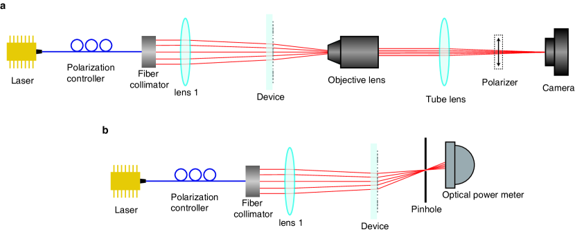
Measurement procedure. We characterized the devices using a setup that is schematically shown in Supplementary Fig. 5a. Light from a 915 nm fibre coupled semiconductor laser was passed through a fibre polarization controller and collimated to generate a Gaussian beam. To collimate the fibre output and generate a Gaussian beams with a beam radius smaller than the device radius, we used a fibre collimation package (Thorlabs F220APC-780) and a lens (Thorlabs LB1676-B with focal length of 10 cm for measuring the devices shown in Fig. 4a and Thorlabs LB1945-B with focal length of 20 cm for the devices shown in Figs. 4b,c and 5). The illumination beam radius on the sample was adjusted by changing the distance between the lens and the sample. The beam radius was set to approximately 35 m for measuring the device shown in Fig. 4a to avoid overlap of the deflected and non-deflected portions of the output light at the measurement plane. To fill most of the device physical aperture, the illumination beam radius was set to 80 m for all other measurements reported in Figs. 4b,c and 5. The objective lens, the tube lens (Thorlabs LB1945-B), and the camera (CoolSNAP K4 from Photometrics) shown in Supplementary Fig. 5a comprise a custom built microscope. We used three different objective lenses to achieve different magnifications. Measurement results shown in Fig. 4a were obtained using a 20X objective lens (Olympus UMPlanFl, NA=0.4), results shown in Figs. 4b and 4c, and Fig. 5a were recorded using a 50X objective lens (Olympus LCPlan N, NA=0.65), and the ones presented in Figs. 5b and 5c were obtained using a 100X objective lens (Olympus UMPlanFl, NA=0.95). The overall microscope magnification for each objective lens was found by imaging a calibration sample with known feature sizes. The polarizer (Thorlabs LPNIR050-MP) was inserted into the setup to confirm the polarization state of the incident light (after removing the device) and the output light. Efficiency values for the devices shown in Figs. 4a,c and 5 were obtained by integrating the light intensity on the camera (i.e. the measured intensity profiles shown in Figs. 4 and 5), subtracting the dark noise, and normalizing it to the integrated intensity recorded when the device was removed. For the device shown in Fig. 4a, only the intensity of the deflected portion of the output light was used for efficiency calculation. To characterize the efficiency of the device shown in Fig. 4b, we used a setup schematically shown in Supplementary Fig. 5b. A 25 m diameter pinhole (Thorlabs P25S) was placed at the focal plane of the device and was aligned such that only the light focused to one of the two focal points could pass through it. To obtain the reported efficiencies, the optical power passed through the pinhole was measured using a power meter (Thorlabs PM100D with Thorlabs S122C power sensor), and was divided by the power of the incident beam which was measured before the device.
References
- (1) Kildishev, A. V., Boltasseva, A. & Shalaev, V. M. Planar photonics with metasurfaces. Science 339, 1232009 (2013).
- (2) Yu, N. & Capasso, F. Flat optics with designer metasurfaces. Nature Mater. 13, 139–50 (2014).
- (3) Yu, N. et al. Light propagation with phase discontinuities: generalized laws of reflection and refraction. Science 334, 333–7 (2011).
- (4) Lin, D., Fan, P., Hasman, E. & Brongersma, M. L. Dielectric gradient metasurface optical elements. Science 345, 298–302 (2014).
- (5) Lin, J., Genevet, P., Kats, M. A., Antoniou, N. & Capasso, F. Nanostructured holograms for broadband manipulation of vector beams. Nano Lett. 13, 4269–74 (2013).
- (6) Vo, S. et al. Sub-wavelength grating lenses with a twist. IEEE Photon. Technol. Lett. 26, 1375–1378 (2014).
- (7) Monticone, F., Estakhri, N. M. & Alù, A. Full control of nanoscale optical transmission with a composite metascreen. Phys. Rev. Lett. 110, 203903 (2013).
- (8) Arbabi, A. & Faraon, A. Fundamental limits of ultrathin metasurfaces (2014). arXiv:eprint 1411.2537.
- (9) Aieta, F. et al. Aberration-free ultrathin flat lenses and axicons at telecom wavelengths based on plasmonic metasurfaces. Nano Lett. 12, 4932–6 (2012).
- (10) Pfeiffer, C. & Grbic, A. Cascaded metasurfaces for complete phase and polarization control. Appl. Phys. Lett. 102, 231116 (2013).
- (11) Fattal, D., Li, J., Peng, Z., Fiorentino, M. & Beausoleil, R. G. Flat dielectric grating reflectors with focusing abilities. Nature Photon. 4, 466–470 (2010).
- (12) Lu, F., Sedgwick, F. G., Karagodsky, V., Chase, C. & Chang-Hasnain, C. J. Planar high-numerical-aperture low-loss focusing reflectors and lenses using subwavelength high contrast gratings. Opt. Express 18, 12606–14 (2010).
- (13) Klemm, A. B. et al. Experimental high numerical aperture focusing with high contrast gratings. Opt. Lett. 38, 3410–3 (2013).
- (14) Aieta, F., Kats, M. A., Genevet, P. & Capasso, F. Multiwavelength achromatic metasurfaces by dispersive phase compensation. Science 347, 1342–1345 (2015).
- (15) Warren, M., Smith, R., Vawter, G. & Wendt, J. High-efficiency subwavelength diffractive optical element in gaas for 975 nm. Opt. Lett. 20, 1441–1443 (1995).
- (16) Lalanne, P., Astilean, S., Chavel, P., Cambril, E. & Launois, H. Design and fabrication of blazed binary diffractive elements with sampling periods smaller than the structural cutoff. JOSA A 16, 1143–1156 (1999).
- (17) Arbabi, A. et al. Controlling the phase front of optical fiber beams using high contrast metastructures - OSA Technical Digest (online). In CLEO: 2014, STu3M.4 (Optical Society of America, San Jose, California, 2014).
- (18) Arbabi, A., Horie, Y., Ball, A. J., Bagheri, M. & Faraon, A. Subwavelength-thick lenses with high numerical apertures and large efficiency Based on high contrast transmitarrays Nature Commun. 6, 7069 (2015).
- (19) West, P. R. et al. All-dielectric subwavelength metasurface focusing lens. Opt. Express 22, 26212 (2014).
- (20) Decker, M. et al. High-efficiency dielectric Huygens’ surfaces. Adv. Opt. Mater. (2015).
- (21) Kikuta, H., Ohira, Y. & Iwata, K. Achromatic quarter-wave plates using the dispersion of form birefringence. Appl. Opt. 36, 1566–1572 (1997).
- (22) Schonbrun, E., Seo, K. & Crozier, K. B. Reconfigurable imaging systems using elliptical nanowires. Nano Lett. 11, 4299–303 (2011).
- (23) Yang, Y. et al. Dielectric meta-reflectarray for broadband linear polarization conversion and optical vortex generation. Nano Lett. 14, 1394–9 (2014).
- (24) Mutlu, M., Akosman, A. E., Kurt, G., Gokkavas, M. & Ozbay, E. Experimental realization of a high-contrast grating based broadband quarter-wave plate. Opt. Express 20, 27966–73 (2012).
- (25) Zhao, Y., Belkin, M. A. & Alù, A. Twisted optical metamaterials for planarized ultrathin broadband circular polarizers. Nature Commun. 3, 870 (2012).
- (26) García-Etxarri, A. et al. Strong magnetic response of submicron silicon particles in the infrared. Opt. Express 19, 4815–26 (2011).
- (27) Evlyukhin, A. B., Reinhardt, C. & Chichkov, B. N. Multipole light scattering by nonspherical nanoparticles in the discrete dipole approximation. Phys. Rev. B 84, 235429 (2011).
- (28) Spinelli, P., Verschuuren, M. A. & Polman, A. Broadband omnidirectional antireflection coating based on subwavelength surface Mie resonators. Nature Commun. 3, 692 (2012).
- (29) Zhan, Q. Cylindrical vector beams: from mathematical concepts to applications. Adv. Opt. Photonics 1, 1 (2009).
- (30) Phelan, C. F., Donegan, J. F. & Lunney, J. G. Generation of a radially polarized light beam using internal conical diffraction. Opt. Express 19, 21793–802 (2011).
- (31) Kozawa, Y. & Sato, S. Generation of a radially polarized laser beam by use of a conical Brewster prism. Opt. Lett. 30, 3063 (2005).
- (32) Swanson, G. J. Binary optics technology: the theory and design of multi-level diffractive optical elements. Tech. Rep., DTIC Document (1989).
- (33) Liu, V. & Fan, S. S4 : A free electromagnetic solver for layered periodic structures. Comput. Phys. Commun. 183, 2233–2244 (2012).
- (34) Born, M. & Wolf, E. Principles of optics (Cambridge University Press, 1999).
Acknowledgement
This work was supported by Caltech/JPL president and director fund (PDF) and DARPA. Yu Horie was supported as part of the DOE “Light-Material Interactions in Energy Conversion” Energy Frontier Research Centre under grand DE-SC0001293 and JASSO fellowship. The device nanofabrication was performed in the Kavli Nanoscience Institute at Caltech.
The authors thank David Fattal and Charles Santori for useful discussion.
Author contributions
A. A. and A. F. conceived the experiment. A. A., Y. H., and M. B. fabricated the samples. A. A. performed the simulations, measurements, and analyzed the data. A. A. and A. F. co-wrote the manuscript. All authors discussed the results and commented on the manuscript.
Additional information
Correspondence and requests for materials should be addressed to A. F. at faraon@caltech.edu
Competing financial interests
The authors declare no competing financial interests.
I Supplementary Information
S1. Arbitrary polarization and phase transformation using symmetric and unitary Jones matrices
Here we show that any arbitrary polarization and phase transformation can always be performed using a unitary and symmetric Jones matrix. We prove this by determining the unitary and symmetric Jones matrix that maps a given input electric field to a desired output electric field . For polarization and phase transformations (i.e. no amplitude modification), the Jones matrix should be unitary since the transmitted power is equal to the incident power and . The general relation between the electric fields of input and output optical waves for normal incidence is expressed as . For a symmetric and unitary Jones matrix we have
| (1a) | |||
| (1b) | |||
where and are the and components of the electric field of the input light, and are the and components of the electric field of the output light, () are the elements of the 22 Jones matrix, and * represents complex conjugation. In deriving Eqs. 1a and 1b, we have used the symmetric properties , and the unitary condition . By multiplying Eq. 1a by and Eq. 1b by we obtain
| (2a) | |||
| (2b) | |||
By adding Eqs. 2a and 2b, using the unitary condition , and taking the complex conjugate of the resultant relation, we find
| (3) |
Finally, by expressing Eqs. 3 and 1a in the matrix form, we obtain
| (4) |
Therefore, for any given and , we can find and from Eq. 4, and and from the symmetry and unitary conditions as
| (5a) | ||||
| (5b) | ||||
Thus, we can always find a unitary and symmetric Jones matrix that transforms any input optical wave to any output optical wave .
S2. Realization of any symmetric and unitary Jones matrices using a uniform birefringent metasurface
Here we show that any symmetric and unitary Jones matrix can be realized using a uniform birefringent metasurface shown in Fig. 2a in the main text, if , , and the angle between one of the principal axis of the metasurface and the axis () could be chosen freely. Any symmetric and unitary matrix is decomposable in terms of its eigenvectors and eigenvalue matrix () as
| (6) |
where superscript T represents the matrix transpose operation. is a real unitary matrix; therefore, it corresponds to an in-plane geometrical rotation by an angle that we refer to as , and since , represents a rotation by . According to Eq. 6, the operation of a metasurface that realizes the Jones matrix can be considered as rotating the electric field of the input wave () by , phase shifting the and components of the rotated respectively by and , and rotating back the rotated and phase shifted vector by angle . Equivalently, can be implemented using a metasurface that imposes phase shifts and to the components of along angles and , respectively. Such a metasurface is realized by starting with a metasurface whose principal axis are along and directions and imparts and phase shifts to and -polarized waves, and rotating it anticlockwise by angle . Therefore, any symmetric and unitary Jones matrix can be realized using a metasurface if its , , and in-plane rotation angle () could be chosen freely.
S3. Independent wavefront control for two orthogonal polarizations
In this section, we derive the necessary condition for the design of a device that imposes two independent phase profiles to two optical waves with orthogonal polarizations. The four elements of the Jones matrix are found uniquely using Eqs. 4 and 5, when the determinant of the matrix on the left hand side of Eq. 4 is nonzero. Therefore, a devices that is designed to map to , converts an optical wave whose polarization is orthogonal to to an optical wave polarized orthogonal to . For example, an optical element designed to generate radially polarized light from polarized input light, will also generate azimuthally polarized light from polarized input light.
In the special case that the determinant of the matrix on the left had side of Eq. 4 is zero we have
| (7) |
and because is unitary we have ; therefore we find where is an arbitrary phase. This special case corresponds to a device that preserves the polarization ellipse of the input light, switches its handedness (helicity), and imposes a phase shift on it. In this case, the matrix is not uniquely determined from Eq. 4, and an additional condition, such as the phase profile for the orthogonal polarization, can be imposed on the operation of the device. Therefore, the device can be designed to realize two different phase profiles for two orthogonal input polarizations.
II Supplementary Figures