Local field corrections to the spontaneous emission in arrays of Si nanocrystals
Abstract
We present a theory of the local field corrections to the spontaneous emission rate for the array of silicon nanocrystals in silicon dioxide. An analytical result for the Purcell factor is obtained. We demonstrate that the local-field corrections are sensitive to the volume fill factor of the nanocrystals in the sample and are suppressed for large values of the fill factor. The local-field corrections and the photonic density of states are shown to be described by two different effective permittivities: the harmonic mean between the nanocrystal and the matrix permittivities and the Maxwell-Garnett permittivity.
pacs:
42.70.Qs, 42.50.-pI Introduction
Modification of the spontaneous emission rate in the electromagnetic environment is well known since the seminal work of Purcell Purcell (1946). This effect has been studied for various systems, including microcavities Kavokin et al. (2006), photonic crystals, and metamaterials Poddubny et al. (2013). Here, we focus on the example of Si nanocrystals in SiO2 matrix Priolo et al. (2014). The Purcell factor, defined as the ratio of the radiative decay rate of a single spherical nanocrystal in SiO2 to that in vacuum, reads Yablonovitch et al. (1988); Delerue and Lannoo (2004):
| (1) |
where is the radiative lifetime in vacuum (calculated neglecting the field screening), and are the dielectric constants of the silicon dioxide matrix and silicon, respectively. The factor in Eq. (1) is determined by the photonic density of states in the matrix. The second factor describes the local field corrections. It is equal to the squared ratio of the electric field inside the (spherical) nanocrystal to the field outside the nanocrystal and can be determined from the solution of a pure electrostatic problem Landau and Lifshitz (1974). Substituting the values and , we obtain , i.e. the field inside the nanocrystal is strongly screened Delerue and Lannoo (2004).
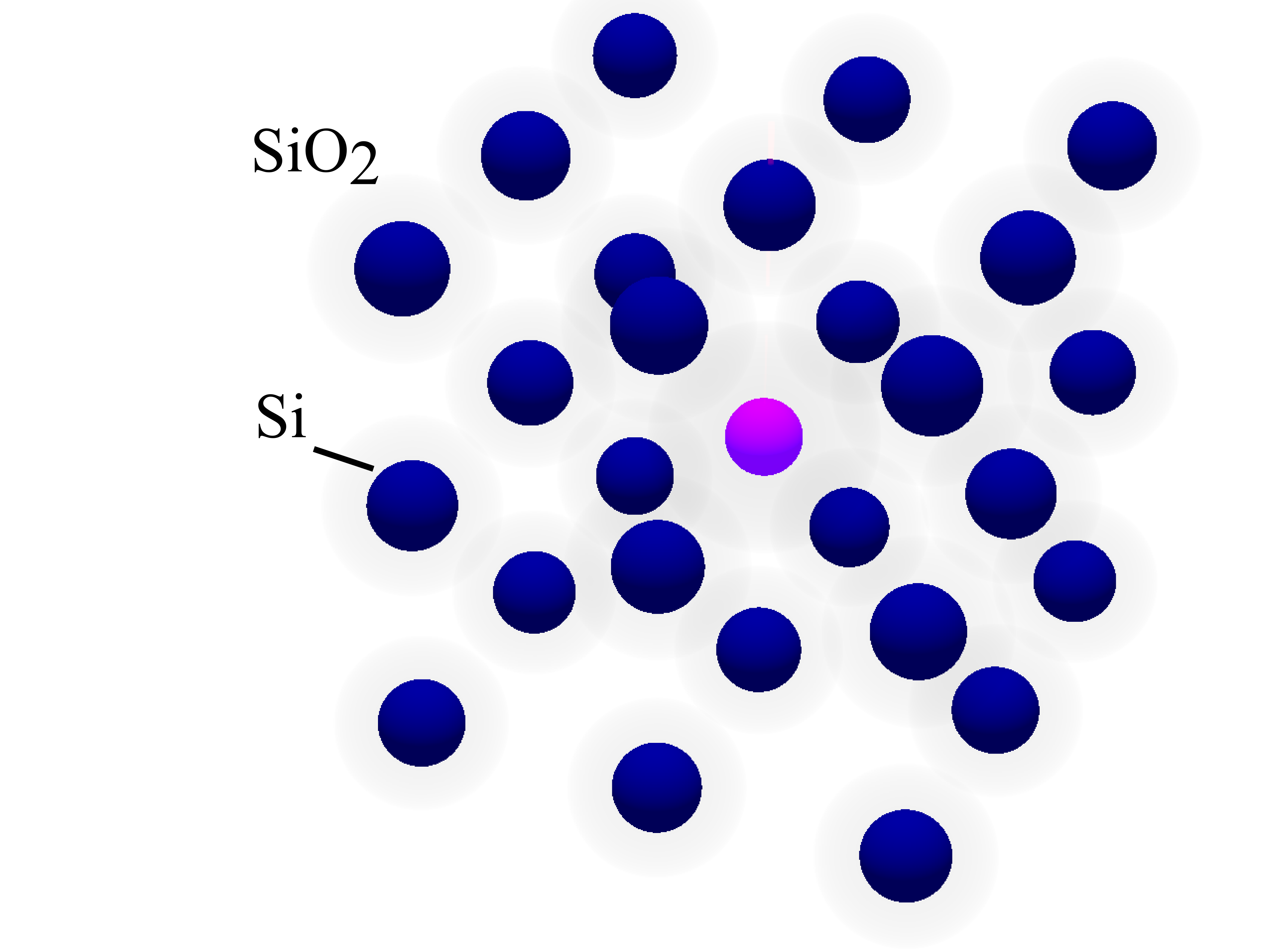
Equation (1) has been obtained for the case of single nanocrystal. In practice, however, one often considers relatively dense samples with the volume fractions of Si exceeding Timmerman et al. (2011); Rens Limpens et al. (2014). Since the permittivity of Si is quite large, the effective dielectric constant of such samples can considerably exceed that of empty SiO2. As a result, one can expect strong modification of the radiative decay rate Eq. (1): both the density of photonic states in the sample and the local field factor should be sensitive to the volume fraction of Si . To the best of our knowledge, this problem has not been examined in the literature. Existing microscopic electromagnetic studies were limited to the case of single emitter and/or different geometries Schuurmans and Lagendijk (2000); Busch et al. (2000); Fussell et al. (2004); Rahmani et al. (2002); Poddubny et al. (2012). In particular, in the previous works Rahmani et al. (2002); Poddubny et al. (2012) the local field corrections have been taken into account, however, the geometry of the problem was quite different. Instead of the emitting nanocrystal, an external interstitial emitter has been introduced into the array of scatterers. In the current manuscript we address the problem of the local field corrections to the spontaneous emission in nanocrystal arrays (see Fig. 1) when the emitter is at the lattice site and the local field corrections are influenced by its neighbors in the lattice.
Solution of this problem is essential for the reliable measurement of the radiative emission rate of the nanocrystals. Typically, the recombination of electron-hole pairs is contributed by both the spontaneous emission and the nonradiative recombination channels. Measurement of the decay kinetics of the photoluminescence only does not allow one to distinguish between these two processes. One of the established Snoeks et al. (1995); Blum et al. (2012); Miura et al. (2006) approaches to separate the effects is to modify the radiative decay rate by placing the emitters close to the dielectric or metallic mirror. Assuming that the nonradiative decay stays the same, one can extract the radiative decay rate from the dependence of the total decay rate on the distance from the mirror. However, the validity of this technique for the dense nanocrystal samples is not yet clear.
II Coupled dipoles model
II.1 Single nanocrystal
We start with re-deriving the classical result Eq. (1) within the framework of the discrete dipole model and a semiclassical approximation. While the spontaneous emission per se is a quantum process, its modification in the medium can be studied semiclassically Ginzburg (1983); Vogel and Welsch (2006). We describe the nanocrystal by the bare dipole polarizability
| (2) |
where the first term accounts for the difference between the background dielectric constants of Si and SiO2 with being the nanocrystal volume. The second term describes the polarization due to the excitonic state with the resonance frequency , the parameter is an effective dipole moment of the transition. Our goal is to determine the complex radiative correction to the frequency , arising due to the interaction with light. To this end, we solve the coupled system of the equation for the total electric field and the material equation for the dipole moment of the nanocrystal :
| (3) | ||||
where is the incident field,
| (4) |
is the tensor Green function, is the light wave vector and denotes the tensor . Evaluating the first of Eqs. (3) at and and combining it with the second one we obtain the equation for the eigenfrequencies of the system:
| (5) |
It should be noted that the real part of the Green function Eq. (4) diverges at the origin. To overcome this problem one has to take into account the finite spread of the emitter. This can be carried out either by replacing the local material relation by the nonlocal one Ivchenko (2005); Goupalov (2003), or, alternatively, by keeping the local material relation but regularizing the Green function at the origin de Vries et al. (1998). Both approaches are equivalent for subwavelength nanocrystals when the dipole approximation holds. Here, we resort to the second approach, which means that at is replaced by the regularized value
| (6) |
Substituting Eq. (6) and Eq. (2) into Eq. (5) we obtain the closed-form equation for the complex eigenfrequency . We use the weak-coupling approximation when the Green function can be evaluated at the resonant frequency . For the nanocrystal with spherical symmetry the solution is three-fold degenerate. The imaginary part of the eigenfrequency in the lowest order in the retardation parameter reads
| (7) |
This is equivalent to the known answer Eq. (1) with the standard expression for the radiative lifetime in vacuum Vogel and Welsch (2006) . The complex polarizability of the nanocrystal with and without excitons, renormalized by the interaction with light and describing the response to the incident field , is given by de Vries et al. (1998)
| (8) |
When the radiative correction term in Eq. (6) for is neglected, the expression for reduces to the well-known electrostatic result Landau and Lifshitz (1974) for the dipole polarizability of the single sphere
| (9) |
Re-derivation of Eq. (7) and Eq. (9) justifies the validity of our approach and provides the route to generalize the technique for the array of nanocrystals.
II.2 Array of nanocrystals
We consider the periodic cubic array with the period , forming the lattice (see Fig. 1). For such system, one can obtain closed-form analytical results in the long-wavelength approximation Purcell and Pennypacker (1973); Sprik et al. (1996); Belov and Simovski (2005); Poddubny et al. (2012); Gorlach et al. (2014). The coupled-dipole equations describing the problem read
| (10) |
with
| (11) |
Here, we take into account the resonant polarization term only in one of the nanocrystals, with and . This corresponds to the situation of strong inhomogeneous broadening of the excitonic resonance. The system Eq. (10) can be equivalently rewritten as
| (12) |
In order to solve the system Eq. (10) the dipole momenta can be expanded over the Bloch eigenmodes
| (13) |
with and the integration being performed over the first Brillouin zone. For the Bloch modes Eqs. (12) become independent,
| (14) |
with
| (15) |
being the interaction constant Belov and Simovski (2005). Solving Eq. (14) for , and substituting the result back to Eq. (13) we obtain the following equation for the eigenfrequency :
| (16) |
The second term in this equation is real. Hence, the Purcell factor, i.e. the normalized spontaneous emission rate, is determined only by the third term. This term is proportional to the identity matrix due to the cubic symmetry of the problem. The final result can be presented as
| (17) |
where and the interaction constant is to be evaluated at the frequency .
It is instructive to analyze Eq. (17) in more detail. First, if the interaction constant is neglected, the result reduces to . This expression is equal to for , in agreement with the result Eq. (1) for a single nanocrystal. Second, for the periodic structure the quantity is real Belov and Simovski (2005). Hence, the imaginary part of Eq. (17) appears only due to the poles determined by the dispersion equation . This is designated by the symbol in the denominator of Eq. (17): the integral is to be calculated by adding the negligibly small quantity in the denominator and then taking the limit . Physically, this means that the energy is carried away from the source only by the photonic eigenmodes of the structure, that satisfy the dispersion equation.
Now we proceed to the analytical evaluation of Eq. (17) in the long-wavelength limit . The wave vectors of the photonic modes responsible for the spontaneous emission are then much smaller than . Hence, the interaction constant can be presented in the Maxwell-Garnett approximation Belov and Simovski (2005) as
| (18) |
where is the unit cell size. Before performing the integration we introduce the effective dielectric constant in the Maxwell-Garnett approximation Lagendijk et al. (1997)
| (19) |
where is obtained from by neglecting the radiative correction term in the Green function Eq. (6). Alternatively, Eq. (19) can be presented as
| (20) |
where is the volume fill factor of the nanocrystals. Expressing the polarizability via from Eq. (19), substituting it into Eq. (17) and calculating the inverse matrix, we obtain
| (21) |
The integration can be performed by introducing the spherical coordinate system for the wave vector . The imaginary part is determined by the residue at . The Purcell factor can be presented as
| (22) | ||||
| (23) |
Equations (22),(23) constitute the central result of this study.
III Results and discussion

We proceed to the detailed analysis of the Purcell factor for the array of nanocrystals Eq. (22). For vanishing fill factor of the nanocrystals, , Eq. (22) reduces to the result for a single nanocrystal, Eq. (1), because . In the general case Eq. (1) and Eq. (22) have two important differences. First, the factor in Eq. (1) is replaced by in Eq. (22). This reflects the modification of the density of photonic states in the medium. Instead of the dielectric constant of the empty matrix , the structure is described by the effective dielectric constant of the nanocrystal array . Second, the local-field factor in Eq. (1) is replaced by the factor in Eq. (22) with the permittivity given by the harmonic mean Eq. (23). Since , the considered permittivities satisfy the following inequality,
| (24) |
which means that
| (25) |
Hence, the role of local field corrections is suppressed for the array of nanocrystals as compared to the empty matrix. This result is quite natural: since the local permittivity outside the nanocrystal increases, the dielectric contrast between the nanocrystal and its surroundings is reduced, and hence, the factor becomes closer to unity. Counterintuitively, the harmonic mean permittivity , that determines the local field corrections , is different from the effective permittivity , that determines the density of photonic states. This can be related to the difference between the far field (described by ) and the near field (described by ). The far field probes the modification of the dielectric environment at the spatial scale larger than the light wavelength, while the near field is sensitive to the immediate environment of the emitting nanocrystal.
These results are illustrated in Fig. 2. Panel (a) presents the dependence of the effective dielectric constants (solid curve) and (dashed curve) on the volume fill factor . Both permittivities grow with from towards , however, is noticeably smaller. It should be noted that both the Maxwell-Garnett approximation and the coupled-dipole model are not applicable for large densities of nanocrystals when the deviation from the point dipole approximation become important Milton (2004). Hence, we limit the range of fill factors in Fig. 2 by the value . Figure 2(b) shows the dependence of the Purcell factor on . The values are smaller than unity due to the strong screening of the field, described by the factor . The solid curve has been calculated according to Eq. (22). The dashed curve has been calculated as , i.e. neglecting the suppression of the local field corrections for large fill factor and overestimating their importance. The dotted curve corresponds to , i.e. it underestimates the role of the local field corrections. We see, that the three curves considerably differ for . Hence, the modification of the local field corrections in the nanocrystal array is an important effect for such relatively dense nanocrystal samples. Our rigorous result Eq. (22) corresponds to the value of the Purcell factor, intermediate between the two naive approximations.
IV Summary
We have developed a theory of spontaneous emission in the dense arrays of Si nanocrystals. By using the discrete dipole approximation we were able to obtaine a closed form analytical answer for the Purcell factor, valid in the long-wavelength approximation when both the size of the nanocrystals and the spacing between them are much smaller than the wavelength of light. This expression reflects (i) the enhancement of the density of photonic states and (ii) the suppression of the local-field corrections when the volume fill factor of the nanocrystals in the sample increases. We demonstrate, that these two effects are described by two different effective permittivities, namely, the Maxwell-Garnett permittivity and the harmonic mean permittivity. While the model is relatively crude and does not account for the disorder, inevitably present in the actual samples, it still provides an important insight in the problem. Our results could be instrumental in optical characterization of the emission kinetics of nanocrystal sample. Moreover, the theory is quite general and could be applied, for instance, for the rapidly developing area of all-dielectric silicon-based nanophotonics Kuznetsov et al. (2012); Staude et al. (2013).
Acknowledgements
This work has been supported by the Russian Science Foundation grant No. 14-12-01067. I acknowledge useful discussions with R. Limpens.
References
- Purcell (1946) E. M. Purcell, Phys. Rev. 69, 681 (1946).
- Kavokin et al. (2006) A. Kavokin, J. Baumberg, G. Malpuech, and F. Laussy, Microcavities (Clarendon Press, Oxford, 2006).
- Poddubny et al. (2013) A. Poddubny, I. Iorsh, P. Belov, and Y. Kivshar, Nature Photonics 7, 948 (2013).
- Priolo et al. (2014) F. Priolo, T. Gregorkiewicz, M. Galli, and T. F. Krauss, Nature Nanotechnology 9, 19 (2014).
- Yablonovitch et al. (1988) E. Yablonovitch, T. J. Gmitter, and R. Bhat, Phys. Rev. Lett. 61, 2546 (1988).
- Delerue and Lannoo (2004) C. Delerue and M. Lannoo, Nanostructures. Theory and Modelling (Springer Verlag, Berling, Heidelberg, 2004).
- Landau and Lifshitz (1974) L. Landau and E. Lifshitz, Electrodynamics of Continuous Media (Pergamon, New York, 1974).
- Timmerman et al. (2011) D. Timmerman, J. Valenta, K. Dohnalova, W. D. A. M. de Boer, and T. Gregorkiewicz, Nature Nanotechnology 6, 710 (2011).
- Rens Limpens et al. (2014) R. Rens Limpens, A. Lesage, P. Stallinga, A. N. Poddubny, M. Fujii, and T. Gregorkiewicz, submitted (2014).
- Schuurmans and Lagendijk (2000) F. J. P. Schuurmans and A. Lagendijk, The Journal of Chemical Physics 113, 3310 (2000).
- Busch et al. (2000) K. Busch, N. Vats, S. John, and B. C. Sanders, Phys. Rev. E 62, 4251 (2000).
- Fussell et al. (2004) D. P. Fussell, R. C. McPhedran, and C. Martijn de Sterke, Phys. Rev. E 70, 066608 (2004).
- Rahmani et al. (2002) A. Rahmani, P. C. Chaumet, and G. W. Bryant, Opt. Lett. 27, 430 (2002).
- Poddubny et al. (2012) A. N. Poddubny, P. A. Belov, P. Ginzburg, A. V. Zayats, and Y. S. Kivshar, Phys. Rev. B 86, 035148 (2012).
- Snoeks et al. (1995) E. Snoeks, A. Lagendijk, and A. Polman, Phys. Rev. Lett. 74, 2459 (1995).
- Blum et al. (2012) C. Blum, N. Zijlstra, A. Lagendijk, M. Wubs, A. P. Mosk, V. Subramaniam, and W. L. Vos, Phys. Rev. Lett. 109, 203601 (2012).
- Miura et al. (2006) S. Miura, T. Nakamura, M. Fujii, M. Inui, and S. Hayashi, Phys. Rev. B 73, 245333 (2006).
- Ginzburg (1983) V. L. Ginzburg, Soviet Physics Uspekhi 26, 713 (1983).
- Vogel and Welsch (2006) W. Vogel and D.-G. Welsch, Quantum Optics (Wiley, Weinheim, 2006).
- Ivchenko (2005) E. L. Ivchenko, Optical Spectroscopy of Semiconductor Nanostructures (Alpha Science International, Harrow, UK, 2005).
- Goupalov (2003) S. V. Goupalov, Phys. Rev. B 68, 125311 (2003).
- de Vries et al. (1998) P. de Vries, D. V. van Coevorden, and A. Lagendijk, Rev. Mod. Phys. 70, 447 (1998).
- Purcell and Pennypacker (1973) E. M. Purcell and C. R. Pennypacker, Astroph. J. 186, 705 (1973).
- Sprik et al. (1996) R. Sprik, B. A. van Tiggelen, and A. Lagendijk, EPL (Europhysics Letters) 35, 265 (1996).
- Belov and Simovski (2005) P. A. Belov and C. R. Simovski, Phys. Rev. E 72, 026615 (2005).
- Gorlach et al. (2014) M. A. Gorlach, A. N. Poddubny, and P. A. Belov, Phys. Rev. B 90, 035106 (2014).
- Lagendijk et al. (1997) A. Lagendijk, B. Nienhuis, B. A. van Tiggelen, and P. de Vries, Phys. Rev. Lett. 79, 657 (1997).
- Milton (2004) G. W. Milton, The Theory of Composites (Cambridge University Press, UK, 2004).
- Kuznetsov et al. (2012) A. I. Kuznetsov, A. E. Miroshnichenko, Y. H. Fu, J. Zhang, and B. Luk’yanchuk, Scientific Reports 2, 492 (2012).
- Staude et al. (2013) I. Staude, A. E. Miroshnichenko, M. Decker, N. T. Fofang, S. Liu, E. Gonzales, J. Dominguez, T. S. Luk, D. N. Neshev, I. Brener, et al., ACS Nano 7, 7824 (2013).