First-Principles Study of Hybrid Graphene and MoS2 Nanocomposites
Abstract
Combining the electronic properties of graphene and molybdenum disulphide (MoS2) monolayers in two-dimensional (2D) ultrathin hybrid nanocomposites have been synthesized experimentally to create excellent electronic, electrochemical, photovoltaic, photoresponsive and memory devices. Here, first-principles calculations are performed to investigate the electronic, electrical and optical properties in hybrid G/MoS2 and G/MoS2/G nanocomposites. It turns out that weak van der Waals interactions dominate between graphene and MoS2 with their intrinsic electronic properties preserved. Interestingly, tunable p-type doping of graphene is very easy to achieve by applying electric fields perpendicular to hybrid G/MoS2 and G/MoS2/G nanocomposites, because electrons can easily transfer from the Dirac point of graphene to the conduction band of MoS2 due to the work function of graphene close to the electronic affinity of MoS2. Vertical electric fields can generate strong p-type but weak n-type doping of graphene, inducing electron-hole pairs in hybrid G/MoS2/G sandwiched nanocomposites. Moreover, improved optical properties in hybrid G/MoS2 and G/MoS2/G nanocomposites are also expected with potential photovoltaic and photoresponsive applications.
pacs:
I Introduction
Graphene, a two-dimensional (2D) sp2-hybridized carbon sheet, has received considerable interest recently owing to its outstanding properties,Scinece_306_666_2004 ; NatureMater_6_183_2007 ; RMP_81_109_2009 ; NatPhotonics_4_611_2010 especially, high carrier mobility, with great potential applications for graphene-based electronic devices, such as field effect transistors (FETs). But, intrinsic electronic properties of graphene depend sensitively on the substrates due to strong graphene-substrate interactions, such as SiO2,NanoLett_7_1643_2007 ; NatPhys_4_144_2008 ; PRL_106_106801_2011 SiC,NatureMater_6_770_2007 ; PRL_99_126805_2007 ; PRL_108_246104_2012 and metal surfaces.PRL_101_026803_2008 ; PRB_79_195425_2009 ; NatureNanotech_6_179_2011 Finding an ideal substrate for graphene remains a significant challenge.
Interestingly, many 2D ultrathin hybrid graphene-based nanocomposites have been widely studied experimentally and theoretically, such as graphene/hexagonal born nitride (G/h-BN),Nature_5_722_2010 ; NatureMater_10_282_2011 ; NanoLett_12_714_2012 graphene/graphitic carbon nitride (G/g-C3N4),JPCC_115_7355_2011 ; JACS_133_8074_2011 ; JACS_134_4393_2012 and graphene/graphitic ZnO (G/g-ZnO).JCP_138_124706_2013 ; JPCC_117_10536_2013 ; JAP_113_054307_2013 These hybrid graphene-based nanocomposites show much more new properties far beyond their simplex components. Furthermore, most of them are ideal substrates for graphene to preserve its intrinsic electronic properties.
Recently, 2D flexible heterostructures consisting of graphene and monolayer molybdenum disulphidePRL_87_196803_2001 ; PRL_105_136805_2010 ; NanoLett_10_1271_2010 ; NatureNanotechnol_6_147_2011 ; ACSNano_6_74_2012 (G/MoS2) have been synthesized experimentallyCC_47_4252_2011 ; ACSNano_5_4720_2011 ; Science_335_947_2012 ; NanoLett_12_2784_2012 ; JACS_134_6575_2012 ; NatureMater_12_246_2013 ; NatureCommun_4_1624_2013 ; ACSNano_7_3246_2013 ; NatureNanotechnol_8_826_2013 ; Nanoscale_6_1071_2014 with great applications in excellent electronic, electrochemical, photovoltaic, photoresponsive and memory devices. Monolayer MoS2 itself is an interesting semiconducting transition metal dichalcogenide, which has been widely studied experimentally and theoreticallyPRL_87_196803_2001 ; PRL_105_136805_2010 ; NanoLett_10_1271_2010 ; NatureNanotechnol_6_147_2011 ; ACSNano_6_74_2012 due to its outstanding structural, electronic and optical properties superior to other 2D materials as graphene substrates. For example, monolayer MoS2 has a appropriate bandgap (1.90 )PRL_105_136805_2010 to achieve a high current on/off ratio of 10000 in G/MoS2 based FETs far superior to vertical G/h-BN heterostructures with an insufficient current on/off ratio of 50 due to the large bandgap (5.97 ) of h-BN.Science_335_947_2012 Most recently, hybrid G/MoS2/G sandwiched nanocomposites have also been synthesized experimentally,Science_340_1311_2013 ; ACSNano_7_7021_2013 showing strong light-matter interactions and large quantum tunneling current modulations in flexible graphene-based FETs superior to hybrid G/MoS2 nanocomposites. Theoretically, only few worksNanoscale_3_3883_2011 ; JPCC_117_15347_2013 have been focused on the structural and electronic of hybrid G/MoS2 nanocomposites. Therefore, a systematic theoretical work on hybrid graphene and MoS2 nanocomposites (G/MoS2 and G/MoS2/G) is very desirable with more exciting new properties to be expected, such as electrical and optical properties.
In the present work, we study structural, electronic, electrical and optical properties in hybrid G/MoS2 and G/MoS2/G nanocomposites using first-principles calculations. Graphene interacts overall weakly with via van der Waals interactions with their intrinsic electronic properties preserved. Applying vertical electric fields is very easy to induce tunable p-type doping of graphene in hybrid G/MoS2 nanocomposites and generate strong p-type but weak n-type doping of graphene in hybrid G/MoS2/G sandwiched nanocomposites. Moreover, hybrid graphene and MoS2 nanocomposites show enhanced optical absorption compared to simplex graphene and MoS2 monolayers.
II Theoretical Models and Methods
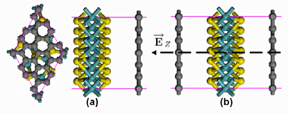
The lattice parameters of graphene and MoS2 monolayers calculated to setup unit cell are (G) = 2.47 Å and (MoS2) = 3.19 Å.Nanoscale_3_3883_2011 ; JPCC_117_15347_2013 In order to simulate hybrid graphene and MoS2 nanocomposites, a 2 2 supercell of graphene (24 carbom atoms) is used to match a supercell of MoS2 (7 sulfur and 14 molybdenum atoms) with a smaller lattice mismatch of about 1% compared with previous theoretical studies.Nanoscale_3_3883_2011 ; JPCC_117_15347_2013 Furthermore, our designed hybrid graphene and MoS2 nanocomposites are consistent with recent experimental observation of a faint moiré structure with high resolution STM images of graphene on MoS2.Nanoscale_6_1071_2014 In this work, both hybrid G/MoS2 and G/MoS2/G nanocomposites are considered as shown in FIG 1. The vacuum space in the direction is about 15 Å to separate the interactions between neighboring slabs.
First-principles calculations are based on the density functional theory (DFT) implemented in the VASP package.PRB_47_558_1993_VASP The generalized gradient approximation of Perdew, Burke, and Ernzerhof (GGA-PBE)PRL_77_1996 with van der Waals (vdW) correction proposed by Grimme (DFT-D2)JCC_27_1787_2006_Grimme is chosen due to its good description of long-range vdW interactions.JPCC_111_11199_2007 ; PCCP_10_2722_2008 ; NanoLett_11_5274_2011 ; PRB_83_245429_2011 ; PRB_85_125415_2012 ; PRB_85_235448_2012 ; PCCP_14_8179_2012 ; PCCP_15_497_2013 ; PCCP_15_5753_2013 ; Nanoscale_5_9062_2013 ; JPCL_4_2158_2013 ; PCCP_2014 As an benchmark, DFT-D2 calculations give a good bilayer distance of 3.25 Å and binding energy of -25 per carbon atom for bilayer graphene, fully agreeing with previous experimentalPR_100_544_1955 ; PRB_69_155406_2004 and theoreticalPRB_85_205402_2012 ; JCP_138_054701_2013 studies. The energy cutoff is set to be 500 . The surface Brillouin zone is sampled with a 5 5 regular mesh and 240 points are used for calculating the tiny band gaps at the Dirac points of silicene. All the geometry structures are fully relaxed until energy and forces are converged to 10-5 and 0.01 /Å, respectively. Dipole correction is employed to cancel the errors of electrostatic potential, atomic forces and total energy, caused by periodic boundary condition.PRB_51_4014_1995_DipoleCorrection The external electric field is introduced in the VASP by the dipole layer method with the dipole placed in the vacuum region of periodic supercell.
To study the optical properties of hybrid graphene and MoS2 nanocomposites, the frequency-dependent dielectric matrix is calculated.PRB_73_045112_2006 The imaginary part of dielectric matrix is determined by a summation over states as
| (1) | ||||
where, is the volume of the primitive cell, is the k point weight, and are the conduction and valence band states respectively, and are the eigenvalues and wavefunctions at the k point respectively, and are the unit vectors for the three Cartesian directions. In order to accurately calculate the optical properties of hybrid graphene and MoS2 nanocomposites, a large 21 21 regular mesh for the surface Brillouin zone, a large number of empty conduction band states (three times more than the number of valence band) and frequency grid points (4000) are adopted. Note that the optical properties of pristine graphene and MoS2 monolayers are crosschecked and consistent with previous theoretical calculations.JCP_139_154704_2013 ; PRB_88_045412_2013
In order to evaluate the stability of hybrid graphene and MoS2 nanocomposites, the interface binding energy is defined as
| (2) |
where, , and represent the total energy of hybrid graphene and MoS2 nanocomposites, pristine graphene and MoS2 monolayers, respectively.
III Results and Discussion
First, we check the structural and electronic properties of pristine graphene and MoS2 monolayers, agreeing well with previous theoretical studies.Nanoscale_3_3883_2011 ; JPCC_117_15347_2013 Pristine graphene monolayer is a zero-gap semiconductor, showing a linear Dirac-like dispersion relation () = around the Fermi level, where F is the Fermi velocity, and F = 0.8106 JCP_139_154704_2013 at the Dirac point of graphene, although GGA-PBE calculations underestimate the Fermi velocity of graphene by 1520%.PRB_76_205411_2007 Pristine MoS2 monolayer is a semiconductor with a direct band gap of 1.64 , although GGA-PBE calculationsPRB_78_235104_2008 slightly underestimate this band gap value (1.90 ).PRL_105_136805_2010
We then study the structural and electronic properties of hybrid graphene and MoS2 nanocomposites as summarized in TABLE I. The equilibrium spacings of 3.37 and 3.36 Å are obtained for hybrid G/MoS2 and G/MoS2/G nanocomposites with corresponding binding energy of -20.5 and 27.0 per atom, respectively. Thus, graphene is physically adsorbed on monolayer MoS2 via weak van der Waals (vdW) interactions, and intrinsic electronic properties of graphene and MoS2 can be preserved in ultrathin hybrid nanocomposites, agreeing well with previous experimentalCC_47_4252_2011 ; ACSNano_5_4720_2011 ; Science_335_947_2012 ; NanoLett_12_2784_2012 ; JACS_134_6575_2012 ; NatureMater_12_246_2013 ; NatureCommun_4_1624_2013 ; ACSNano_7_3246_2013 ; NatureNanotechnol_8_826_2013 ; Nanoscale_6_1071_2014 ; Science_340_1311_2013 ; ACSNano_7_7021_2013 and theoreticalNanoscale_3_3883_2011 ; JPCC_117_15347_2013 studies.
| DFT-D2 | ||
|---|---|---|
| G/MoS2 | 3.37 | -20.5 |
| G/MoS2/G | 3.36/3.36 | -27.0 |
Electronic band structures of hybrid graphene and MoS2 nanocomposites are shown as FIG 2. We find that linear Dirac-like dispersion relation around the Fermi levels of graphene is still preserved in hybrid G/MoS2 and G/MoS2/G nanocomposites, though tiny band gaps (1 ) are opened at the Dirac points of graphene, which are significantly lower than thermal fluctuation (about 25 ) at room temperature and trend to vanish in experiments. Note that induced graphene band gaps are typically sensitive to other external conditions, such as interlayer separation,JCP_139_154704_2013 showing that the band gap values increase gradually with the interlayer separation decrease, thus tunable, with a potential for flexible graphene-based FETs.
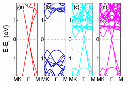
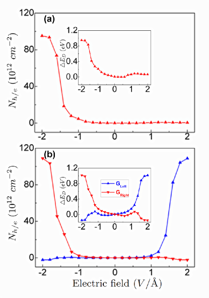
High-performance field-effect tunneling transistors have been achieved experimentallyScience_335_947_2012 ; NatureCommun_4_1624_2013 ; NatureNanotechnol_8_826_2013 ; Science_340_1311_2013 ; ACSNano_7_7021_2013 in hybrid graphene and MoS2 nanocomposites. Thus, the electronic properties of hybrid G/MoS2 and G/MoS2/G nanocomposites affected by applying vertical electric fields are very desirable as shown in FIG 3. Interestingly, negative vertical electric fields can induce p-type doping of graphene in hybrid G/MoS2 nanocomposites. But, positive electric fields almost have on effect on the electronic properties of hybrid G/MoS2 nanocomposites. This is because electrons can easily from the Dirac point of graphene to the conduction band of MoS2 but difficulty from the valence band of MoS2 to the Dirac point of graphene due to the work function (4.3 )JCP_138_124706_2013 of graphene close to the electronic affinity (4.2 )NatureCommun_4_1624_2013 of monolayer MoS2. Interestingly, vertical electric fields can generate strong p-type but weak n-type doping of graphene at both negative and positive electric fields due to the symmetry in hybrid G/MoS2/G nanocomposites. Based on the linear dispersion around the Dirac point of graphene,RMP_81_109_2009 the charge carrier (hole or electron) concentration of doped graphene can be estimated by the following equationJCP_138_124706_2013
| (3) |
where is the shift of graphene’s Dirac point () relative to the Fermi level (), that is = - . The calculated charge carrier concentrations in hybrid G/MoS2 and G/MoS2/G nanocomposites are shown in FIG 4. These values are more than 3 orders of magnitude larger than the intrinsic charge carrier concentration of graphene at room temperature ( = /6 = 6 ).PRL_108_246104_2012 Furthermore, the doping charge carrier concentrations of graphene in hybrid nanocomposites are increased with the vertical electric fields. Therefore, the field-effect in hybrid graphene and MoS2 nanocomposites is effective and tunable for high-performance FETs and p-n junctions.Science_340_1311_2013 ; ACSNano_7_7021_2013
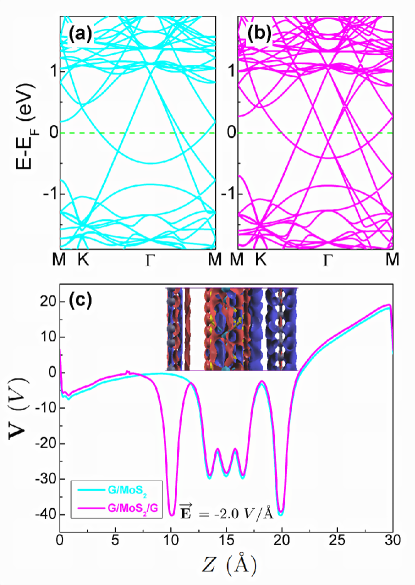
As an example, electronic band structures of hybrid G/MoS2 and G/MoS2/G nanocomposites and their corresponding XY-averaged electrostatic potential (V) in the direction at a vertical electric field of -2.0 /Å are shown in FIG 4. Charge-transfer complexes are formed in hybrid graphene and MoS2 nanocomposites affected by vertical electric fields. The differential charge density ( = (G/MoS2) - (G) - (MoS2)) of hybrid G/MoS2 and G/MoS2/G nanocomposites are shown in FIG 3c. Particularly, electron-hole pairs are well separated in hybrid G/MoS2/G sandwiched nanocomposites with more excellent applicationsScience_340_1311_2013 ; ACSNano_7_7021_2013 compared with hybrid G/MoS2 nanocomposites. Note that the band gap values at graphene’s Dirac points in hybrid G/MoS2 and G/MoS2/G nanocomposites are almost not affected by vertical electric fields, different to bilayer graphene.Nature_459_820_2009 ; NanoLett_10_426_2010
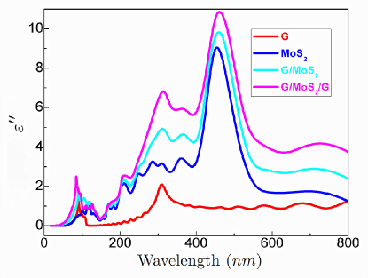
Besides commonly focused electronic structures in hybrid G/MoS2 nanocomposites,Nanoscale_3_3883_2011 ; JPCC_117_15347_2013 we also study the optical properties in hybrid G/MoS2 and G/MoS2/G nanocomposites due to their photovoltaic and photoresponsive applications.ACSNano_7_3246_2013 ; NatureNanotechnol_8_826_2013 ; Nanoscale_6_1071_2014 ; Science_340_1311_2013 Note that pristine graphene and MoS2 monolayers themselves display outstanding optical properties,NatPhotonics_4_611_2010 ; NanoLett_10_1271_2010 but interlayer interaction and charge transfer in graphene-based hybrid nanocomposites can induce new optical transitions.JACS_134_4393_2012 In optical property calculations, the imaginary part of dielectric function for pristine graphene and MoS2 monolayers as well as corresponding hybrid graphene and MoS2 nanocomposites are evaluated as shown in FIG 5. In fact, monolayer MoS2 shows much stronger optical absorption than graphene in the visible light region (200 800 ). Moreover, hybrid graphene and MoS2 nanocomposites exhibit more strongly enhanced light response, especially hybrid G/MoS2/G sandwiched heterostructures, compared with simplex graphene and MoS2 monolayers, because electrons can now be easily and directly excited from the Dirac point of graphene to the conduction band of MoS2.
IV Summary and Conclusions
In summary, structural, electronic, electrical and optical
properties in hybrid G/MoS2 and G/MoS2/G nanocomposites are
studied via first-principles calculations. Graphene interacts
overall weakly with via van der Waals interactions with their
intrinsic electronic properties preserved. Applying vertical
electric fields is very easy to induce tunable p-type doping of
graphene in hybrid G/MoS2 nanocomposites and generate p-type and
n-type doping of graphene in hybrid G/MoS2/G sandwiched
nanocomposites. Moreover, hybrid G/MoS2 and G/MoS2/G
nanocomposites display enhanced optical absorption compared to
simplex graphene and MoS2 monolayers. With excellent electronic,
electrical and optical properties combined, ultrathin hybrid
graphene and MoS2 nanocomposites are expected to be with great
applications in efficient electronic, electrochemical, photovoltaic,
photoresponsive and memory devices.
V ACKNOWLEDGMENTS
This work is partially supported by the National Key Basic Research Program (2011CB921404), by NSFC (21121003, 91021004, 2123307, 21222304), by CAS(XDB01020300). This work is also partially supported by the Scientific Discovery through Advanced Computing (SciDAC) program funded by U.S. Department of Energy, Office of Science, Advanced Scientific Computing Research and Basic Energy Sciences (W. H.). We thank the National Energy Research Scientific Computing (NERSC) center, and the USTCSCC, SC-CAS, Tianjin, and Shanghai Supercomputer Centers for the computational resources.
References
- (1) K. S. Novoselov, A. K. Geim, S. V. Morozov, D. Jiang, Y. Zhang, S. V. Dubonos, I. V. Grigorieva, and A. A. Firsov, Scinece 306, 666 (2004).
- (2) A. K. Geim and K. S. Novoselov, Nature Mater. 6, 183 (2007).
- (3) A. H. C. Neto, F. Guinea, N. M. R. Peres, K. S. Novoselov, and A. K. Geim, Rev. Mod. Phys. 81, 109 (2009).
- (4) F. Bonaccorso, Z. Sun, T. Hasan, and A. C. Ferrari, Nature Photon. 4, 611 (2010).
- (5) M. Ishigami, J. H. Chen, W. G. Cullen, M. S. Fuhrer, and E. D. Williams, Nano Lett. 7, 1643 (2007).
- (6) J. Martin, N. Akerman, G. Ulbricht, T. Lohmann, J. H. Smet, K. von Klitzing, and A. Yacoby, Nature Phys. 4, 144 (2008).
- (7) N. T. Cuong, M. Otani, and S. Okada, Phys. Rev. Lett. 106, 106801 (2011).
- (8) S. Y. Zhou, G.-H. Gweon, A. V. Fedorov, P. N. First, W. A. de Heer, D.-H. Lee, F. Guinea, A. H. C. Neto, and A. Lanzara, Nature Mater. 6, 770 (2007).
- (9) F. Varchon, R. Feng, J. Hass, X. Li, B. N. Nguyen, C. Naud, P. Mallet, J.-Y. Veuillen, C. Berger, E. H. Conrad, and L. Magaud, Phys. Rev. Lett. 99, 126805 (2007).
- (10) J. Ristein, S. Mammadov, and T. Seyller, Phys. Rev. Lett. 108, 246104 (2012).
- (11) G. Giovannetti, P. A. Khomyakov, G. Brocks, V. M. Karpan, J. van den Brink, and P. J. Kelly, Phys. Rev. Lett. 101, 026803 (2008).
- (12) P. A. Khomyakov, G. Giovannetti, P. C. Rusu, G. Brocks, J. van den Brink, and P. J. Kelly, Phys. Rev. B 79, 195425 (2009).
- (13) F. Xia, V. Perebeinos, Y. Lin, Y. Wu, and P. Avouris, Nature Nanotech. 6, 179 (2011).
- (14) C. R. Dean, A. F. Young, I. Meric, C. Lee, L. Wang, S. Sorgenfrei, K. Watanabe, T. Taniguchi, P. Kim, K. L. Shepard, and J. Hone, Nature Nanotech. 5, 722 (2010).
- (15) J. Xue, J. Sanchez-Yamagishi, D. Bulmash, P. Jacquod, A. Deshpande, K. Watanabe, T. Taniguchi, P. Jarillo-Herrero, and B. LeRoy, Nature Mater. 10, 282 (2011).
- (16) K. H. Lee, H.-J. Shin, J. Lee, I. Lee, G.-H. Kim, J.-Y. Choi, and S.-W. Kim, Nano Lett. 12, 714 (2012).
- (17) Q. J. Xiang, J. G. Yu, and M. Jaroniec, J. Phys. Chem. C 115, 7355 (2011).
- (18) X.-H. Li, J.-S. Chen, X. Wang, J. Sun, and M. Antonietti, J. Am. Chem. Soc. 133, 8074 (2011).
- (19) A. Du, S. Sanvito, Z. Li, D. Wang, Y. Jiao, T. Liao, Q. Sun, Y. H. Ng, Z. Zhu, R. Amal, and S. C. Smith, J. Am. Chem. Soc. 134, 4393 (2012).
- (20) W. Hu, Z. Li, and J. Yang, J. Chem. Phys. 138, 124706 (2013).
- (21) W. Geng, X. Zhao, H. Liu, and X. Yao, J. Phys. Chem. C 117, 10536 (2013).
- (22) X. Guo and Y. G. Zhou, J. Appl. Phys. 113, 054307 (2013).
- (23) M. V. Bollinger, J. V. Lauritsen, K. W. Jacobsen, J. K. Nørskov1, S. Helveg, and F. Besenbacher, Phys. Rev. Lett. 87, 196803 (2001).
- (24) K. F. Mak, C. Lee, J. Hone, J. Shan, and T. F. Heinz, Phys. Rev. Lett. 105, 136805 (2010).
- (25) A. Splendiani, L. Sun, Y. Zhang, T. Li, J. Kim, C.-Y. Chim, G. Galli, and F. Wang, Nano Lett. 10, 1271 (2010).
- (26) B. Radisavljevic, A. Radenovic, J. Brivio, V. Giacometti, and A. Kis, Nature Nanotech. 6, 147 (2011).
- (27) Z. Yin, H. Li, H. Li, L. Jiang, Y. Shi, Y. Sun, G. Lu, Q. Zhang, X. Chen, and H. Zhang, ACS Nano 6, 74 (2012).
- (28) K. Chang and W. Chen, Chem. Commun. 47, 4252 (2011).
- (29) K. Chang and W. Chen, ACS Nano 5, 4720 (2011).
- (30) L. Britnell, R. V. Gorbachev, R. Jalil, B. D. Belle, F. Schedin, A. Mishchenko, T. Georgiou, M. I. Katsnelson, L. Eaves, S. V. Morozov, N. M. R. Peres, J. Leist, A. K. Geim, K. S. Novoselov, and L. A. Ponomarenko, Science 335, 947 (2012).
- (31) Y. Shi, W. Zhou, A.-Y. Lu, W. Fang, Y.-H. Lee, A. L. Hsu, S. M. Kim, K. K. Kim, H. Y. Yang, L.-J. Li, J.-C. Idrobo, and J. Kong, Nano Lett. 12, 2784 (2012).
- (32) Q. Xiang, J. Yu, and M. Jaroniec, J. Am. Chem. Soc. 134, 6575 (2012).
- (33) W. J. Yu, Z. Li, H. Zhou, Y. Chen, Y. Wang, Y. Huang, X. Duan, X. Nature Mater. 12, 246 (2013).
- (34) M. S. Choi, G. H. Lee, Y. J. Yu, D. Y. Lee, S. H. Lee, P. Kim, J. Hone, and W. J. Yoo, Nature Commun. 4, 1624 (2013).
- (35) S. Bertolazzi, D. Krasnozhon, and A. Kis, ACS Nano 7, 3246 (2013).
- (36) K. Roy, M. Padmanabhan, S. Goswami, T. P. Sai, G. Ramalingam, S. Raghavan, and A. Ghosh, Nature Nanotech. 8, 826 (2013).
- (37) H. Diaz, R. Addou, and M. Batzill, Nanoscale 6, 1071 (2014).
- (38) L. Britnell, R. M. Ribeiro, A. Eckmann, R. Jalil, B. D. Belle, A. Mishchenko, Y.-J. Kim, R. V. Gorbachev, T. Georgiou, S. V. Morozov, A. N. Grigorenko, A. K. Geim, C. Casiraghi, A. H. C. Neto, K. S. Novoselov, Science 340, 1311 (2013).
- (39) N. Myoung, K. Seo, S. J. Lee, and G. Ihm, ACS Nano 7, 7021 (2013).
- (40) Y. Ma, Y. Dai, M. Guo, C. Niu, and B. Huang, Nanoscale 3, 3883 (2011).
- (41) X. D. Li, S. Yu, S. Q. Wu, Y. H. Wen, S. Zhou, and Z. Z. Zhu, J. Phys. Chem. C 117, 15347 (2013).
- (42) G. Kresse and J. Hafner, Phys. Rev. B 47, 558 (1993).
- (43) J. P. Perdew, K. Burke, and M. Ernzerhof, Phys. Rev. Lett. 77, 3865 (1996).
- (44) S. Grimme, J. Comput. Chem. 27, 1787 (2006).
- (45) S. Grimme, C. Muck-Lichtenfeld, and J. Antony, J. Phys. Chem. C 111, 11199 (2007).
- (46) J. Antony and S. Grimme, Phys. Chem. Chem. Phys. 10, 2722 (2008).
- (47) N. Kharche and S. K. Nayak, Nano Lett. 11, 5274 (2011).
- (48) J. Sławińska, P. Dabrowski, and I. Zasada, Phys. Rev. B 83, 245429 (2011)
- (49) R. Kagimura, M. S. C. Mazzoni, and H. Chacham, Phys. Rev. B 85, 125415 (2012).
- (50) Y. Ma, Y. Dai, M. Guo, and B. Huang, Phys. Rev. B 85, 235448 (2012).
- (51) L. Yuan, Z. Li, J. Yang, and J. G. Hou, Phys. Chem. Chem. Phys. 14, 8179 (2012).
- (52) L. Yuan, Z. Li, and J. Yang, Phys. Chem. Chem. Phys. 15, 497 (2013).
- (53) W. Hu, X. Wu, Z. Li, and J. Yang, Phys. Chem. Chem. Phys. 15, 5753 (2013).
- (54) W. Hu, X. Wu, Z. Li, and J. Yang, Nanoscale 5, 9062 (2013).
- (55) L. Chen, L. Wang, Z. Shuai, and D. Beljonne, J. Phys. Chem. Lett. 4, 2158 (2013).
- (56) W. Hu, N. Xia, X. Wu, Z. Li, and J. Yang, Phys. Chem. Chem. Phys. (2014).
- (57) Y. Baskin and L. Mayer, Phys. Rev. 100, 544 (1955).
- (58) R. Zacharia, H. Ulbricht, and T. Hertel, Phys. Rev. B 69, 155406 (2004).
- (59) R. E. Mapasha, A. M. Ukpong, and N. Chetty, Phys. Rev. B 85, 205402 (2012).
- (60) W. Hu, Z. Li, and J. Yang, J. Chem. Phys. 138, 054701 (2013).
- (61) G. Makov and M. C. Payne, Phys. Rev. B 51, 4014 (1995).
- (62) M. Gajdos̆, K. Hummer, and G. Kresse, Phys. Rev. B 73, 045112 (2006).
- (63) W. Hu, Z. Li, and J. Yang, J. Chem. Phys. 139, 154704 (2013).
- (64) A. Molina-Sánchez, D. Sangalli, K. Hummer, A. Marini, and L. Wirtz, Phys. Rev. B 88, 045412 (2013).
- (65) M. Calandra and F. Mauri, Phys. Rev. B 76, 205411 (2007).
- (66) S. Lany and A. Zunger, Phys. Rev. B 78, 235104 (2008).
- (67) Y. Zhang, T.-T. Tang, C. Girit, Z. Hao, M. C. Martin, A. Zettl, M. F. Crommie, Y. R. Shen, and F. Wang, Nature 459, 820 (2009).
- (68) C.-H. Park and S. G. Louie, Nano Lett. 10, 426 (2010).