Graphene vertical cascade interband terahertz and infrared photodetectors
Abstract
We propose and evaluate the vertical cascade terahertz and infrared photodetectors based on multiple-graphene-layer (GL) structures with thin tunnel barrier layers (made of tungsten disulfide or related materials). The photodetector operation is associated with the cascaded radiative electron transitions from the valence band in GLs to the conduction band in the neighboring GLs (interband- and inter-GL transitions). We calculate the spectral dependences of the responsivity and detectivity for the vertical cascade interband GL- photodetectors (I-GLPDs) with different number of GLs and doping levels at different bias voltages in a wide temperature range. We show the possibility of an effective manipulation of the spectral characteristics by the applied voltage. The spectral characteristics depend also on the GL doping level that opens up the prospects of using I-GLPDs in the multi-color systems. The advantages of I-GLPDs under consideration are associated with their sensitivity to the normal incident radiation, weak temperature dependence of the dark current as well as high speed of operation. The comparison of the proposed I-GLDs with the quantum-well intersubband photodectors demonstrates the superiority of the former, including a better detectivity at room temperature and a higher speed. The vertical cascade I-GLDs can also surpass the lateral p-i-n GLDs in speed.
I Introduction
The GL-based heterostructures with the thin barrier layers made of Boron Nitride (hBN), Tungsten Disulfide (WS2), and other transition metal dichalcogenides have recently attracted a considerable interest. Several novel devices have been proposed and realized [1-14]. Due to the gapless energy spectrum of the GLs in such structures (similar to that single-GLs and non-Bernal stacked twisted GLs in the multiple-GL structures 15 ), such heterostructures can be used in terahertz (THz) and infrared (IR) photodetectors. The GL-structures with the tunneling transparent inter-GL barriers can be particularly useful in the novel THz and IR photodetectors surpassing or complementing other GL-based photodetectors [16-24] and photodetectors based on more standard semiconductor materials 25 .
In this paper, we propose and evaluate the vertical intersubband THz and IR photodetectors based on the Bernal-stacked multiple-GL structures with tunneling barrier layers using the cascade of the interband inter-GL radiative transitions The cascade of the electron tunneling and radiative-assisted tunneling processes supports the vertical dark current and photocurrent between the top and bottom GLs (playing the role of the emitter and collector). The advantages of these photodetectors include the voltage control of their spectral characteristics (at low temperatures), a relatively high responsivity and detectivity (especially in the photodetectors with a relatively large number of GLs), a high speed of operation, and the possibility of operation in the frequency range (from 6 to 10 THz), where using more conventional materials (e.g., A3B5 compounds) is hindered by the optical phonon absorption.
II Structure of I-GLPDs and their operation principle
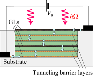
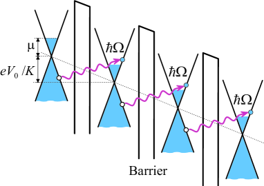
Figure 1 shows the structure of the vertical intersubband GL-photodetector (I-GLPD) under consideration. It consists of several n-doped GLs separated by thin (tunneling-transparent) barrier layers of WS2 or similar material. The bias voltage applied between the extreme GLs serving as the emitter (top GL) and collector (bottom GL), respectively. Figure 2 shows the device band diagram under bias (several GL-structure periods). As seen from Fig.2, the energy gaps between the GLs are equal to , where is the number of the inter-GL barriers in the device.
Absorption by the I-GLPD of the normally incident photons with the energy polarized in the GL plane, the absorption of a portion the photons is accompanied by the electron transitions between the neighboring GLs (see the wavy arrows in Fig. 2). Such direct but inter-GL transitions produce the inter-GL photocurrent. At low temperatures, the spectral range, for the effective interband inter-GL radiative transitions is given by the following inequalities:
| (1) |
where is the electron Fermi energy in the GLs determined by the donor density and (to some extent) by the device temperature . For the degenerate electron gas in the GLs ( where is the Boltzmann constant) , where
| (2) |
Here cm/s is the characteristic velocity of electrons in GLs.
The reverse transitions with the emission of a photon with the energy are suppressed (at sufficiently low temperatures) due to the Pauli blocking. The interband intra-GL transitions are also possible. However, at a certain relation between the photon energy , Fermi energy , and the inter-GL potential drop , these transitions can also be essentially blocked due to the Pauli principle, particularly at low temperatures. This blocking mechanism is also effective for the radiative transitions to the GLs with a higher potential energy,
The interband transitions within the same GL can result in heating of the electron system 26 , particularly at . However, due to a weak temperature dependence of the inter-GL tunneling 26 ; 27 , the pertinent contribution to the inter-GL current turns out to be relatively small if the Fermi energy is much smaller that the barrier height (equal to the conduction band-offset, , between the GL and the barrier material), so that the thermionic emission over the barrier is insignificant. We exclude this case from our consideration here.
Due to the electric field in the top and bottom GLs, the electron densities and, hence, the Fermi energies, and , in these GLs differ from . Taking into account the neutrality of the internal GLs, at low relatively temperatures and at not too strong bias voltages,
| (3) |
Here , where is the electron charge, is the thickness of the barrier layers, and is their dielectric constant. However, a deviation of and from virtually does not affect the results obtained in the following and is disregarded.
III Photocurrent and responsivity
Considering the absorption of normally incident radiation causing the vertical (conserving the electron momentum) interband inter-GL transitions, the photocurrent density , which is proportional to the difference in the rates of the electron transitions from the upper to the lower GLs and the reverse transitions, can be presented as
| (4) |
Here is the characteristic (independent of the photon energy) coefficient of the interband absorption of normally incident electromagnetic radiation associated with the vertical transitions in GLs (see, for example, 15 ), is the speed of light, is the inter-GL overlap integral, is the photon flux of the incident radiation ( is the THz or IR power density), and
| (5) |
is the voltage-dependent Pauli blocking factor, where and is the unity step function: for and for . The factors and in the present form appear due to the linear dependences of the densities of states on the energy in the valence and conductance bands. Similar factor results in the photon energy dependence of the interband inter-GL absorption coefficient in GL structures at the transverse voltage in contrast to the interband intra-GL absorption coefficient (the latter is independent of the photon energy 15 ). In Eq. (4) we have disregarded the reflection of the incident radiation from the top of the GL-structure. The effect of the radiation reflection can easily accounted for by the proper renormalization of the quantity . We have also disregarded any ”superlattice” effects, in particular, the formation of the energy gap because due to the presence of the electric field in the barrier layers leading to the Stark-ladder electron propagation. The applicability of Eq. (4) for the I-GLPDs with relatively large number of the barrier can be limited by the case when the intensity of the radiation weakly decreases with its penetration into the depth of the GL-structure, i.e., by a relatively low absorption in each GL (see below).
The quantity in Eq. (4) is a function of the spacing between GLs , see, Appendix A): , where , is the band offset, and is the effective mass in the barrier. Assuming eV, of the free electron mass 29 , and nm, we obtain . At low temperatures, the factor and inside and outside the interval given by inequalities (1), respectively.
Using Eqs. (4) and (5), we arrive at the following expression for the GLPD responsivity (current responsivity measured in the A/W units):
| (6) |
with
| (7) |
As seen from Eqs. (6) and (7), the I-GLPD responsivity is independent of the number of GLs. Similar situation occurs in quantum-well infrared photodetectors (QWIPs) with the photoexited and injected electrons moving perpendicular to the multiple-QW structure [30-32] (although the dependence on the number of QWs occurs due to the damping of the radiation caused by its absorption in the depth of the multiple-GL structure, the contact effects, and at elevated modulation frequencies and radiation powers 31 ; 33 ; 34 ).

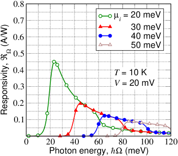
At low temperatures , Eq. (6) yields the spectral dependences with a pronounced maximum in the range . In particular, in the limit , one obtains if and if or .
Figures 3 and 4 show the spectral dependences calculated using Eq. (6) for the I-GLPDs with a WS2 barrier of the thickness nm (), for different Fermi energies: meV at K and mV and 20 mV. As seen, the spectral dependences of the responsivity at K exhibit relatively narrow virtually symmetrical (at mV) and markedly asymmetrical (at mV) peaks. The position centers of these peaks are determined by the Fermi energy (), while their widths is determined by the bias voltage (). The positions of the peak maxima are shifted toward smaller photon energies (). As it was pointed out above, a steep roll-off of the responsivity at and is due to the Pauli blocking of the interband inter-GL radiative transitions outside the indicated photon energy range. Such a blocking is essential in the cases corresponding to Fig. 3 because of a pronounced degeneracy of the electron gas in GLs and a steep variation of the electron distribution function at chosen values of the Fermi energy and the temperature.
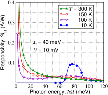
A temperature increase leads to a substantial smearing of the electron distribution function and the responsivity peaks. As a result, the spectral characteristics of the I-GLPD responsivity become monotonic functions of the photon energy at sufficiently high temperatures. Indeed, at relatively high temperatures (), from Eq. (6) we obtain
| (8) |
with
| (9) |
at , and
| (10) |
at . As follows from Eqs. (8) - (10), at elevated temperatures, (via the dependence of on the photon energy).
Figure 5 shows the transformation of the responsivity vs. photon energy dependences with increasing temperature: the smearing of the responsivity maxima (compare the curves for K and 100 K) and transition to the monotonic dependences given by Eq. (10). As seen from Fig. 5, at the low end of the photon spectrum, the responsivity increases with the temperature in agreement with Eq. (10).
According to Figs. 3 - 5, I-GLPDs exhibit fairly different spectral characteristics at low and elevated temperatures with a rather high values of the responsivity in both temperature ranges.
IV Dark current and dark current limited detectivity
Taking into account the Fermi-Dirac statistics of electrons and their linear dispersion relation in GLs, the electron tunneling current between the neighboring GLs at (a strong degeneracy of the electrons in GLs) can be presented in the following simplified form:
| (11) |
In the opposite case (), one obtains
| (12) |
The quantity in Eqs. (11) and (12) is the characteristic escape time from one GL to another. Due to the non-alignment of the Dirac points at the applied voltage, such transitions are possible if they are accompanied by the variation of the electron momentum due to the electron scattering caused by disorder 26 ; 27 . We roughly estimate the escape time as , where is the electron momentum relaxation time. As follows from Eqs. (11) and (12), the dark current is a slow (non-exponential) function of the temperature. Some reinforcement of the temperature dependence in comparison with that given by Eq. (10) might arise from a decrease in with increasing (due to a decreasing vs dependence). As an example, setting meV and s and assuming for WS2 barriers , s (see Appendix B), at low temperatures and at K we obtain from Eqs. (11) and (12) A/cm2 and A/cm2, respectively.
Considering that the noise current is given by , where is the bandwidth, the photodetector dark current limited detectivity can be calculated using the following formula:
| (13) |
where is the device area and is the current gain (both photoelectric and dark current gain). In the I-GLPDs under consideration, in which the transitions occur only between the neighboring GLs, (see, for example, 34 ). Taking into account that , , and , we obtain (for fixed )
| (14) |
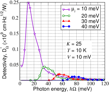
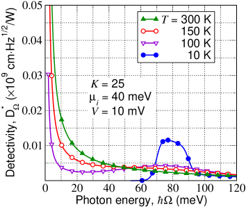
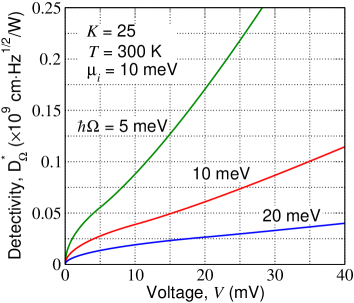
Figures 6 and 7 show the detectivity of the I-GLPDs with different values of the Fermi energy (different donor densities ) at different temperatures calculated using Eq. (6) with Eqs. (11) - (13). One can see that the spectral dependences of qualitatively repeat those of .
V Manipulation of the I-GLPD characteristics and their optimization
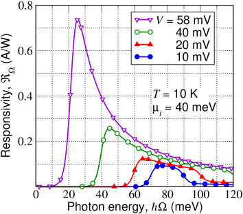
As follows from the above formulas for the I-GLPD responsivity and detectivity, these quantities are determined by the Fermi energy (doping level of GLs), the energy of the incident photons , the temperature , and the bias voltage . This provides an opportunity to optimize the I-GLPD characteristics for different application. According to Figs. 3 -7, the spectral dependences of the responsivity and detectivity at low temperatures (at about K and lower) are located in rather narrow ranges of the photon energy, which are determined by the Fermi energy, i.e., by the donor density in GLs. It opens up the prospect to create GL-based multicolor photodetectors, particularly those operating the spectral range where the operation of the detectors based on A3B5 materials is hindered by the optical phonon absorption. The width of spectral peaks can be decreased by using lower bias voltages (down to , i.e., down to mV at K). An increase in the bias voltage leads to lower dark current [see Eq. (11)] and, hence, in a rise in the detectivity. Figure 8 shows a pronounced rise in the peak responsivity with increasing bias voltage. As seen, an increase in the voltage leads also to a marked transformation of the spectral characteristic and a pronounced shift of the peak position toward smaller photon energies.
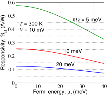
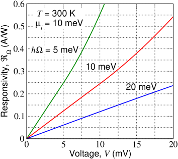
A pronounced variation of the I-GLPD responsivity and detectivity at elevated temperatures also opens up the possibility of the characteristics manipulation and the photodetector optimization. Figures 9 and 10 show the room temperatures responsivity versus the Fermi energy and the bias voltage. Figure 11 shows the I-GLPD detectivity as a function of the bias voltage. Comparing Fig. 9 and 10, one can see that while the responsity is a linear function of the bias voltage (in the voltage range under consideration), the detectivity exhibits a sub-linear behavior. This is because of an increase in the dark current with increasing voltage.
Although the I-GLPD responsivity is practically independent of the number of the inter-GL barriers (and the number of GLs ) in the device structure if this number is not too large, an increase in this number leads to an marked enhancement of the I-GLPD detectivity. The dependence of on appears when the intensity of the incident radiation decreases as the radiation is absorbed by the GLs which are closer to the illuminated device surface. At low temperatures when the Pauli blocking is pronounced and , such effect becomes pronounces when approaches unity. It implies, that the reasonable value of is . When , as a function of saturates. At elevated temperatures, the interband intra-GL absorption is essential, so that the pertinent limitation reads . At marked absorption of the radiation when is large, the electric fields in the barrier layers can be somewhat different (larger in the barrier layers remote from the irradiated surface). This can result in some modification of the obtained formulas (however, not leading to significant changes of the obtained characteristics) which is out of the scope of this work.
VI Comparison with quantum-well and some other photodetectors
The I-GLPD structure resembles the structures of quantum-well infrared photodetectors (QWIPs) and THz quantum-well detectors (THz-QWDs) with multiple QWs. Although QWIPs and THz-QWDs use mainly the photoexcitation from the bound states to the continuum states (in contrast to I-GLDs exploiting the inter-GL tunneling), it makes sense to compare their characteristics. As follows from the obtained results, I-GLPDs at low temperatures ( K)and photon energy meV exhibit the responsivity on the order of 0.1 A/W (see Figs. 3 and 4).
At the photon energy meV (corresponding to the radiation wavelength m) in the temperature range K, GaAs-AlGaAs THz-QWLs studied in Ref. 35 exhibit A/W at K, whereas I-GLPDs with the parameters corresponding to Figs. 3 and 5 exhibits A/W and 0.25 A/W at K and 300K, respectively. The detectivity of the latter THz-QWDs based on the 60-QW structure at meV and K was reported to be cm Hz1/2/W. As seen from Fig. 6, the I-GLPD detectivity at the same photon energy and the temperature reaches the value of cm Hz1/2/W, i.e, five times higher.
However, an increase in the bias voltage to mV (see Fig. 10) and an increase in from to 60 yields the same (at K) as in the THz-QWD in question (at K). The responsivities of a GaAs-AlGaAs THz-QWD 36 and an I-GLPD (see Fig. 8) for meV (m or THz) and K can be close to each other depending on the voltage and can be equal to A/W.
At room temperature in the range meV, covering the photon energy range which is not accessible by A3B5 based detectors due to optical phononabsorption (the region from 33 to 37 meV for GaAs-AlGaAs devices 36 ), I-GLDs could demonstrate rather reasonable values of the responsivity about of 30 - 75 mA/W with a modest detectivity on the order of cm Hz1/2/W(see Figs. 5 and 7).
Due to the possibility of a relatively high-speed operation of QWIPs, they are considered as candidates for the communication systems with the modulation frequencies in the sub-THz range. The QWIP responsivity as a function of the modulation frequency is mainly determined by the electron transit time across the structure and the probability of the electron capture into the QWs. The theoretical estimates and experimental data show the possibility of the QWIPs effective operation up to about hundred GHz 34 ; 37 ; 38 . However in such a range of the modulation frequencies the photoelectric gain is suppressed, so that the QWIP responsivity is much smaller than at low modulation frequencies.
One of the most remarkable features of the I-GLDs is their high-speed operation associated with short inter-GL tunneling times. There are different complex approaches to determine the characteristic tunneling time (see, for example, 37,38 and the speed of devices using the tunneling effects. We assume that the speed of the I-GLPD operation, i.e., the maximum frequency of the radiation modulation should be at least much smaller than , where is the inter-GL tunneling time. Following to Buttiker and Landauer 39 ; 40 , we assume that , where is the electron effective mass in the barrier. For the WS2 barrier width of 1.32 nm, setting eV and of the free electron mass, we obtain fs. This implies that THz, so that the I-GLPDs can operate up to several THz modulation frequencies. For high speed applications, it is desirable to provide a I-GLPD impedance of Ohm. Using Eqs. (11) and (12) and the consequent estimates for low and room temperatures, respectively, we obtain Ohm, where is the I-GLPD area. Therefore, to match the 50 Ohm impedance, for the number of the inter-GL barriers , one needs m2.
The THz- and IR-PDs based on the GL structures with lateral p-i-n junctions (called the lateral p-i-n GLPDs), exploiting the inter-band intra-GL photoexitation of electrons and holes, considered previously 18 ; 23 can exhibit a substantially higher responsivity. However, the speed of their operation is limited (below 25 - 50 GHz) by relatively long electron and hole transit time between the p- and n-regions. Hence, the vertical I-GLPDs can surpass the lateral p-i-n GLPDs in speed in the responsivity can surpass the latter in the speed of operation, even though they have a smaller responsivity.
Thus, the I-GLPDs exhibit sufficiently high responsivity and detectivity at room temperature and can surpass other THz- and IR-PDs in the operation speed. One can anticipate the applications of the I-GLDs in analog transmission systems with the THz or mid-IR carrier frequencies and sub-THz or even THz modulation frequencies.
VII Conclusions
We propose the cascade vertical I-GLPDs based on multiple-GL structures with thin tunnel-transparent barrier layers and exploiting the interband inter-GL radiative transitions. These devices should be able to operate in the THz and mid-infrared spectral ranges. Using the developed device model, we calculated the I-GLPD responsivity and detectivity as functions of the photon energy, the bias voltage, and the number of GLs in the structure in a wide range of temperatures (from cryogenic to room temperatures) and evaluated the I-GLPD speed of operation. We demonstrated that the I-GLPD characteristics strongly depend on the GL doping level and can be effectively controlled by the bias voltage. The I-GLPD can exhibit a sufficiently high responsivity (about several tenth of A/W) both at low and room temperatures and a reasonable detectivity at room temperature, surpassing or competing with other THz and IR-photodetectors. Due to the tunneling origin of the photocurrent and dark current, the THz I-GLPDS and mid-IR I-GLPDs could achieve a higher speed of operation than the existing photodetectors. These new devices can be used in the analog optical communication systems with the sub-THz and THz modulation frequencies.
Appendix A. Inter-GL overlap integral
The envelope wave functions, and , depending on the coordinate in the direction perpendicular to the GL plane for two neighboring GLs can be presented as
| (15) |
Here
| (16) |
where , is the conduction band offset between the barrier material and GLs, and is the effective mass in the barrier. Neglecting the overlap of the wave functions of the distant GLs, the probability of the photon absorption accompanied by the electron transition between the valence band in one GL to the conduction band in the neighboring one can be presented as
| (17) |
where
| (18) |
is the overlap integral and .
Appendix B. Escape time
Using the experimental data from 5 , one can estimate the escape time in graphene-BN-graphene structure. Knowing the peak (resonant) current nA at the bias voltage V, the device area m2, and the electron and hole densities cm-2, we obtain the inter-GL tunneling escape time s. To estimate the inter-GL tunneling escape time, , in graphene-WS2-graphene structure, we take into account that according to the Bardeen tunneling Hamiltonian approach, ,where , and are the thickness and the height of the barrier, and is the effective mass in the intermediate (barrier) material. Thus, the ratio of tunneling escape times and in BN- and WS2- structures can be presented as
| (19) |
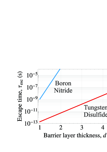
From the measurements of thickness-dependent resistivity of BN tunnel barriers we know nm-1 41 . The obtained tunneling escape time s corresponds to four layers of hBN, which converts to nm nm. Known also graphene-WS2 band structure parameters eV, , we can plot the dependence of on thickness shown in Fig. 12. As seen from Fig. 12, at nm we obtain s, i.e., the value close to that used in the main text. Since our way of extracting provides only the leading exponent, hence the agreement between two approaches is quite reasonable.
Acknowledgments
This work was supported by the Japan Society for promotion of Science (Grant-in-Aid for Specially Promoting Research ), Japan. V. R., M. R., and D.S. acknowledge the support by the Russian Scientific Foundation (Project ). The work by A.D. was also supported by the Dynasty Foundation, Russia. The work at the University at Buffalo was supported by the National Science Foundation TERANO and the Air Force Office of Scientific Research grants. The work at RPI was supported by the US Army Research Laboratory Cooperative Research Agreement.
References
- (1) A. K. Geim and I. V. Grigorieva, “Van der Waals heterostructures,”Nature 499, 419-425 (2013). doi:10.1038/nature12385.
- (2) M. Liu, X. Yin, and X. Zhang, “Double-layer graphene optical modulator,”Nano Lett. 12,1482-1485 (2012).
- (3) L. Britnell, R. V. Gorbachev, R. Jalil, B.D . Belle, F. Shedin, A. Mishenko, T. Georgiou, M. I. Katsnelson, L. Eaves, S. V. Morozov, N. M. R. Peres, J. Leist, A. K. Geim, K. S. Novoselov, and L. A. Ponomarenko, “Field- effect tunneling transistor based on vertical graphene heterostructures,”Science 335, 947-950 (2012).
- (4) T. Georgiou, R. Jalil, B. D. Bellee, L. Britnell, R. V. Gorbachev, S. V. Morozov, Y.-J. Kim, A. Cholinia, S. J. Haigh, O. Makarovsky, L. Eaves, L. A. Ponomarenko, A. K. Geim, K. S. Nonoselov, and A. Mishchenko, “Vertical field-effect transistor based on graphene-WS2 heterostructures for flexible and transparent electronics,”Nature Nanotechnology 7, 100-103 (2013).
- (5) L. Britnell, R. V. Gorbachev, A. K. Geim, L. A. Ponomarenko, A. Mishchenko, M. T. Greenaway, T. M. Fromhold, K. S. Novoselov, and L. Eaves, “Resonant tunneling and negative differential conductance in graphene transistors,”Nature Comm. 4, 1794–1799 (2013).
- (6) V. Ryzhii, T. Otsuji, M. Ryzhii, V. G. Leiman, S. O. Yurchenko, V. Mitin, and M. S. Shur, “Effect of plasma resonances on dynamic characteristics of double-graphene layer optical modulators,”J. Appl. Phys. 112, 104507 (2012).
- (7) V. Ryzhii, T. Otsuji, M. Ryzhii, and M. S. Shur, “Double graphene-layer plasma resonances terahertz detector,”J. Phys. D: Appl. Phys. 45, 302001 (2012).
- (8) V. Ryzhii, A. Satou, T. Otsuji, M. Ryzhii, V. Mitin, and M. S. Shur, “Dynamic effects in double-graphene-layer structures with inter-layer resonant-tunneling negative differential conductivity,”J. Phys. D: Appl. Phys. 46, 315107 (2013).
- (9) V. Ryzhii, M. Ryzhii, V. Mitin, M. S. Shur, A. Satou, and T. Otsuji, “Terahertz photomixing using plasma reso- nances in double-graphene-layer structures,”J. Appl. Phys. 113, 174506 (2013).
- (10) V. Ryzhii, A. A. Dubinov, V. Ya. Aleshkin, M. Ryzhii, and T. Otsuji, “Injection terahertz laser using the resonant inter-layer radiative transitions in double-graphene-layer structure,”Appl. Phys. Lett. 103, 163507 (2013).
- (11) V. Ryzhii,A. A. Dubinov, T.Otsuji, V.Ya. Aleshkin, M. Ryzhii, and M. S. Shur, “Double-graphene-layer terahertz laser: concept, characteristics, and comparison,”Opt. Exp. 21, 31560 (2013)
- (12) V. Ryzhii, T.Otsuji, V.Ya. Aleshkin, A. A. Dubinov, M. Ryzhii, V. Mitin, and M. S. Shur, “Voltage-tunable terahertz and infrared photodetectors based on double-graphene-layer structures,”Appl. Phys. Lett. 104, 104505 (2014).
- (13) C.-H. Liu, Y.-C. Chang, T. B. Norris, and Z. Zhong, “Graphene photodetectors with ultra-broadband and high responsivity at room temperature,”Nature Nanotech. 9, 273-278 (2014).
- (14) C. Oh Kim, S. Kim. D. H. Shin, S. S. Kang, J. M. Kim, C. W. Jang, S. S.J, J.S. Lee, Ju H. Kim. S.-Ho Choi, and E. Hwang, “High photoresponsivity in an all-graphene p-n vertical junction photodetector,”Nat. Com. 5, 3249 (2014).
- (15) A. H. Castro Neto, F. Guinea, N. M. R. Peres, K.S. Novoselov, and A. K. Geim, “The electronic properties of graphene,”Rev. Mod. Phys. 81, 109-162 (2009).
- (16) F. T. Vasko and V. Ryzhii, “Photoconductivity of intrinsic graphene,”Phys. Rev. B 77, 195433 (2008).
- (17) J. Park,Y. H. Ahn, and C. Ruiz-Vargas, “Imaging of photocurrent generation and collection in single-layer graphene,”Nano Lett. 9, 1742–1746 (2009).
- (18) V. Ryzhii, M. Ryzhii, V. Mitin, and T.Otsuji, “Terahertz and infrared photodetection using p-i-n multiple-graphene-layer structures,”J. Appl. Phys. 107, 054512 (2010).
- (19) T. Mueller, F. N. A. Xia, and P. Avouris, “Graphene photodetectors for high-speed optical communications,”Nature Photon. 4, 297–301 (2010).
- (20) M. Furchi, A. Urich, A. Pospischil, G. Lilley, K. Unterrainer, H. Detz, P.Klang, A. M. Andrews, W. Schrenk, G. Strasser, and T. Mueller, “Microcavity-integrated graphene photodetector,”Nano Lett. 12, 2773–2777 (2012).
- (21) X. Gan, R.-J. Shiue, Y.Gao, I. Meric, T. F. Heinz, K. Shepard, J. Hone, S. Assefa, and D. Englund, “Chip-integrated ultrafast graphene photodetector with high responsivity,”Nature Photon. 7, 888–891 (2013).
- (22) F. Bonaccorso, Z. Sun, T, Hasan, and A.C. Ferrari, “Graphene photonics and optoelectronics,”Nature Photon. 4, 611-621 (2010).
- (23) V. Ryzhii, N. Ryabova, M. Ryzhii, N. V. Baryshnikov, V. E. Karasik, V. Mitin, and T. Otsuji, “Terahertz and infrared photodetectors based on multiple graphene layer and nanoribbon structures,”Opto-Electronics Review 20,15-25 (2012).
- (24) A. Tredicucci and M. S. Vitiello,“Device concepts for graphene-based terahertz photonics,”IEEE J. Sel. Top. Quantum Electron 20, 8500109 (2014).
- (25) A. Rogalski, “Recent progress in infrared detector technologies,”Infrared Phys. Technol. 54, 136-154 (2011).
- (26) V. Ryzhii, M. Ryzhii, V. Mitin, A. Satou, and T. Otsuji, “Effect of heating and cooling of photogenerated electron-hole plasma in optically pumped graphene on population inversion,”Jpn. J. Appl. Phys. 50, 094001 (2011).
- (27) R. M. Feenstra, D. Jena, and G. Gu, “Single-particle tunneling in doped graphene-insulator-graphene junctions,”J. Appl. Phys. 111, 043711 (2012).
- (28) F. T. Vasko, “Resonant and nondissipative tunneling in independently contacted graphene structures,”Phys. Rev.B 87, 075424 (2013).
- (29) H. Shi, H. Pan, Y.-W. Zhang, and B. Yakobson, “Quasiparticle band structures and optical properties of strained monolayer MoS2 and WS2,”Phys. Rev. B 87, 155304 (2013).
- (30) H. C. Liu,“Photoconductive gain mechanism of quantum well intersubband infrared detechors,”Appl. Phys. Lett. 60, 1507 (1992).
- (31) V. Ryzhii, “Characteristics of quantum-well infrared photodetectors,”J. Appl. Phys. 81, 6442 (1997).
- (32) K. K. Choi, The physics of Quantum Well Infrared Photodetectors, (World Scientific, 1997).
- (33) V. Ryzhii and H. C. Liu, “Contact and space-charge effects in quantum well infrared photodetectors,”Jpn. J. Appl. Phys. 38, 5815 (1999).
- (34) V. Ryzhii, I. Khmyrova, and M. Ryzhii, “Impact of transit-time and capture effects on high-frequency performance of multiple quantum-well infrared photodetectors,”IEEE Trans. Electron Devices 45, 293-298 (1998).
- (35) M. Graf, G. Scalari, D. Hofstetter, J. Faist, H. Beere, E. Linfeld, D. Ritchie, and G. Davies, “Terahertz range quantum well infrared photodetector,”Appl. Phys. Lett. 84, 475-477 (2004)
- (36) H. C. Liu, C. Y. Song, A. J. SpringThorpe, and J. C. Cao, “Terahertz quantum-well photodetector,”Appl. Phys. Lett. 84, 4068-4070 (2004).
- (37) H. C. Liu, J. Li, E. R. Brown, K. A. McIntosh,K. B. Nichols, and M. J. Manfra, “Quantum well intersubband heterodyne infrared detection up to 82 GHz,”Appl. Phys. Lett. 67, 1594-1596 (1995).
- (38) V. Ryzhii, “High-frequency performance of single quantum well infrared photodetector at high power densities,”IEEE Trans. Electron Devices 45, 1797 - 1803 (1998).
- (39) S. D. Ganichev, E. Ziemann, Th. Gleim, W. Prettl, I. N. Yassievich, V. I. Perel, I. Wilke, and E. E. Haller, “Carrier tunneling in high-frequency electric fields,”Phys. Rev. Lett. 80, 2409-2412 (1998).
- (40) P. C. W. Davies, “Quantum tunneling time,”Am. J. Phys. 73, 23-27 (2005);
- (41) M. Buttiker and R. Landauer, “Traversal time for tunneling,”Phys. Rev. Lett. 49, 1739 (1992).
- (42) A. L. Burin, Y. A. Berlin, and M. A. Rathner, “Semiclassical theory for dissipative tunneling through a molecular wire,”Ann. N.Y. Acad. Sci. 960 240–248 (2002).
- (43) L. Britnell, R. V. Gorbachev, R. Jalil, B. D. Belle, F. Schedin, M. I. Katsnelson, L. Eaves, S. V. Morozov, A. S. Mayorov, N. M. R. Peres, A. H. Castro Neto , J. Leist, A. K. Geim, L. A. Ponomarenko, and K. S. Novoselov, “Electron Tunneling through ultrathin Boron Nitride crystalline barriers,”Nano Lett. 12, 1707-1710 (2012).