Present address: ]Department of Crystalline Materials Science, Nagoya University, Chikusa, Nagoya 464-8603, Japan
Highly textured oxypnictide superconducting thin films on metal substrates
Abstract
Highly textured NdFeAs(O,F) thin films have been grown on ion beam assisted deposition (IBAD)-MgO/Y2O3/Hastelloy substrates by molecular beam epitaxy. The oxypnictide coated conductors showed a superconducting transition temperature () of 43 K with a self-field critical current density () of at 5 K, more than 20 times higher than powder-in-tube processed SmFeAs(O,F) wires. Albeit higher as well as better crystalline quality than Co-doped BaFe2As2 coated conductors, in-field of NdFeAs(O,F) was lower than that of Co-doped BaFe2As2. These results suggest that grain boundaries in oxypnictides reduce significantly compared to that in Co-doped BaFe2As2 and, hence biaxial texture is necessary for high .
pacs:
74.70.Xa, 81.15.Fg, 74.78.-w, 74.25.Sv, 74.25.F-Electron or hole doped Fe2As2 (Ba and Sr) and Fe(Se,Te) show high upper critical fields with low anisotropies at low temperatures that offer a unique possibility for high field magnet applicationsPutti et al. (2010); Li, Si, and Dimitrov (2011). Thanks to the recent progress of processing technology, powder-in-tube (PIT) processed Fe2As2 yields high performance of in-field critical current density ()Weiss et al. (2012); Gao et al. (2012, 2014). Furthermore, Co-doped BaFe2As2 and Fe(Se,Te) on ion beam assisted deposition (IBAD)-MgO/Y2O3/Hastelloy with comparable to those on single crystalline substrates have been demonstrated, although the texture quality of the formers is inferior to the lattersIida et al. (2011); Katase et al. (2011a); Si et al. (2013); Trommler et al. (2012a). These results indicate that properties are quite robust against grain boundaries (GBs) in those materials. Indeed, the critical angle for Co-doped BaFe2As2 at which starts to being degraded is twice as large as cupratesKatase et al. (2011b); Iida et al. (2013a).
On the other hand, FeAs(O,F) (Sm, Nd) is expected to have potentially higher than other Fe-based superconductors due to the highest around 55 KRen et al. (2008); Uemura et al. (2012) among the Fe-based superconductors except for monolayer FeSeHe et al. (2013). However, the level of in PIT-processed SmFeAs(O,F) wire is around even in low fields at 4.2 KFujioka et al. (2011), much lower than Fe2As2 wiresWeiss et al. (2012); Gao et al. (2012, 2014). A fundamental reason for the low in oxypnictide may be due to higher sensitivity against the grain misorientation than other Fe-based superconductors, since FeAs(O,F) (Sm, Nd) has more anisotropic crystal structure and superconducting properties, which resembles high- cuprates. Those facts imply that biaxial textured forms are necessary for high , indicating that the 2nd generation YBa2Cu3O7 coated conductor technology might be suitable for realizing oxypnictide superconducting wires. However, no studies on oxypnictide coated conductors have been reported to date due presumably to the difficulties in fabricating epitaxial FeAs(O,F) thin films on technical substrates.
Here we report on a preparation of NdFeAs(O,F) thin films on MgO-templated Hastelloy by means of molecular beam epitaxy (MBE). By comparing with similar studies on Co-doped BaFe2As2 coated conductorsIida et al. (2011), we point out the necessity of biaxial texture in oxypnictide wires and tapes for high .
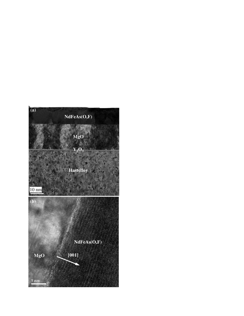
The NdFeAs(O,F) thin films were prepared on IBAD-MgO/Y2O3/Hastelloy by MBE. The IBAD-MgO/Y2O3/Hastelloy has been provided by iBeam Materials, IncSheehan et al. (2011). A mother compound of NdFeAsO was deposited on MgO templated Hastelloy, followed by the deposition of a NdOF cap layer for F diffusion to the NdFeAsO layer. The detailed fabrication can be found in Ref. Kawaguchi et al., 2011. The respective thickness of NdFeAs(O,F) superconducting layer, MgO template and Y2O3 buffer layer were approximately 90 nm, 180 nm and 10 nm confirmed by cross-sectional transmission electron microscope (TEM), which will be shown later.
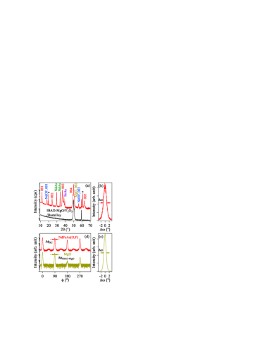
Phase purity and texture quality of the films were examined by x-ray diffraction (Fig. 1). The - scan, fig. 1 (a), shows 00 reflections of NdFeAs(O,F) and NdOF together with the 002 reflection of MgO, indicative of -axis texturing. Albeit the film was -axis oriented, NdAs, FeAs and unidentified impurity phase were detected. The - scan for the 005 reflection of NdFeAs(O,F) in fig. 1 (b) shows a full width at half maximum (FWHM, ) of 1.72∘, which is a similar value to the textured MgO template[(), fig. 1 (c)]. The 102 -scans of NdFeAs(O,F) reveal a small amount of 45∘ in-plane rotated grains, as shown in fig. 1 (d). However, the main reflections were observed at every 90∘, indicative of highly biaxial textured NdFeAs(O,F) films. Here, the epitaxial relation is identified as (001)[100]NdFeAs(O,F)(001)[100]MgO. The average of NdFeAs(O,F) and MgO are 3.38∘ and 2.88∘, respectively. Hence and of NdFeAs(O,F) are similar to those of the underlying MgO template, indicating that the texture is well transferred to NdFeAs(O,F). We have also confirmed that the NdOF cap layer is biaxially textured and its epitaxial relation is (001)[110]NdOF(001)[100]NdFeAs(O,F), which is an observation similar to SmFeAs(O,F) thin filmsIida et al. (2013b).
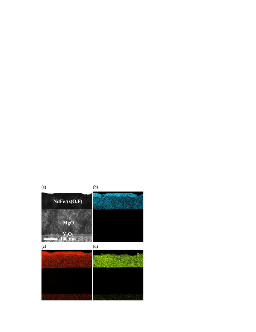
In order to check the homogeneity of the NdFeAs(O,F), microstructural investigation by TEM together with elemental mappings were carried out (fig. 2). In the superconducting layer, some areas have different contrast, which originates from misoriented grains transferred from the underlying MgO templates. As can be seen in fig. 3(a), the MgO layer with white and black in-contrast yields different types of NdFeAs(O,F) grains (i.e., texture transferring from the buffer layer). It is further obvious from fig. 2(a) that trapezoid shaped NdOF layer was grown on NdFeAs(O,F), which is proved by the elemental mappings shown in fig. 2(b) and (c) [i.e., high concentration of both Nd and F] and x-ray - scan shown in fig. 1 (a). Whilst Nd is homogeneous in the superconducting layer, Fe is segregated in the vicinity of the interface [fig. 2 (d)]. Although it is less clear, we note that the area where Fe is segregated seems to be also rich in F.
Shown in fig. 3(b) is the high-resolution TEM image of the NdFeAs(O,F) thin film in the vicinity of the MgO textured template / NdFeAs(O,F) film interface. Clearly a relatively sharp interface is observed between NdFeAs(O,F) and MgO, which is similar to the Co-doped Ba-122 and Fe(Se,Te) thin films on MgO single crystalline substrates prepared by pulsed laser depositionHanawa et al. (2012); Hiramatsu et al. (2012). These results indicate that MgO single crystalline substrates or textured MgO templates are suitable for epitaxial growth of Fe-based superconducting thin films, similarly to CaF2 substrateTsukada et al. (2011); Kurth et al. (2013); Uemura et al. (2012); Ichinose et al. (2014).
The NdFeAs(O,F) film exhibits a of 43 K at which spliting between zero field-cooled (ZFC) and field-cooled (FC) branches of the normalized magnetization curves is observed as shown in fig. 4(a). Here magnetic measurements have been carried out by means of a superconducting quantum interference device (SQUID, Quantum Design) magnetometer and the data were normalized to the ZFC value at 8.5 K. On the other hand, zero resistance was observed at 37 K, measured in a Physical Property Measurement System (PPMS, Quantum Design) by a four-probe method [fig. 4(b)]. This difference is due to a large bias current of 100 mA, leading to a shift of zero resistance temperature to lower temperatures. A sudden increase in the resistance before the superconducting transition is a general observation for films on conducting substrates, where the resistivity of the films in the normal state is higher than that of the substratesTrommler et al. (2012b).
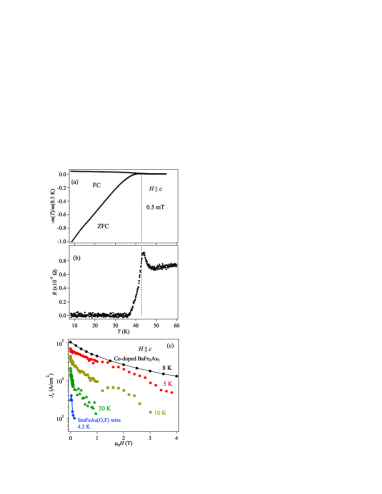
Shown in fig. 4(c) is in-field property of the NdFeAs(O,F) coated conductor measured by a magnetization method using a SQUID magnetometer. Magnetic was evaluated by the following formula: , where is the difference between the magnetic moments observed in the magnetic hysteresis loops for increasing and decreasing field cycles, and are the film dimensions for the -plane, and is the superconducting volumeChen and Goldfarb (1989). As can be seen in fig. 4(c), the self-field of NdFeAs(O,F) coated conductor reaches at 5 K, which is more than 20 times higher than PIT-processed SmFeAs(O,F)Fujioka et al. (2011). Additionally, the oxypnictide coated conductor shows better in-field performance than PIT-processed SmFeAs(O,F). However, of NdFeAs(O,F) film on MgO single crystalline substrate exceeds even at 35 T () at 4.2 KTarantini et al. , indicating that there is much room for optimization. Compared to the Co-doped BaFe2As2 coated conductorIida et al. (2011), the level of for NdFeAs(O,F) is relatively low. Note that the zero resistance temperature of Co-doped BaFe2As2 is 17.5 K, much lower than that of NdFeAs(O,F). Furthermore, in-field for Co-doped BaFe2As2 shown in fig. 4(c) was measured at 8 K. By considering the same reduced temperature (i.e., for Co-doped BaFe2As2), one can expect that of NdFeAs(O,F) at 16.9 K, which is supposed to be located between the curves measured at 10 and 20 K, is reduced significantly by only small magnetic fields. It is also worth mentioning that the value of NdFeAs(O,F) is smaller than that of Co-doped BaFe2As2Iida et al. (2011), as shown in Table 1. These results indicate that NdFeAs(O,F) shows weak-link behavior, which necessitates biaxial texture for high . Nevertheless bicrystal experiments on FeAs(O,F) are necessary to quantitatively characterize the GBs properties.
| Films | ||
|---|---|---|
| NdFeAs(O,F) | ||
| Co-doped BaFe2As2 |
In summary, textured NdFeAs(O,F) thin films have been realized on IBAD-MgO/Y2O3/Hastelloy substrates by MBE. The oxypnictide coated conductors showed a of 43 K with a self-field of at 5 K, more than 20 times higher than PIT processed SmFeAs(O,F) wires. However, the current-limiting effects by GBs in FeAs(O,F) seem to be more serious than in Fe2As2 and Fe(Se,Te). Hence it is necessary to align grains biaxially in oxypnictide wires and tapes for high .
Acknowledgements.
The authors thank M. Kühnel and U. Besold for their technical support. The research leading to these results has received funding from European Union’s Seventh Framework Programme (FP7/2007-2013) under grant agreement number 283141 (IRON-SEA). This research has been also supported by Strategic International Collaborative Research Program (SICORP), Japan Science and Technology Agency.References
- Putti et al. (2010) M. Putti, I. Pallecchi, E. Bellingeri, M. R. Cimberle, M. Tropeano, C. Ferdeghini, A. Palenzona, C. Tarantini, A. Yamamoto, J. Jiang, J. Jaroszynski, F. Kametani, D. Abraimov, A. Polyanskii, J. D. Weiss, E. E. Hellstrom, A. Gurevich, D. C. Larbalestier, R. Jin, B. C. Sales, A. S. Sefat, M. A. McGuire, D. Mandrus, P. Cheng, Y. Jia, H. H. Wen, S. Lee, and C. B. Eom, Supercond. Sci. Technol. 23, 034003 (2010).
- Li, Si, and Dimitrov (2011) Q. Li, W. Si, and I. K. Dimitrov, Rep. Prog. Phys. 74, 124510 (2011).
- Weiss et al. (2012) J. D. Weiss, C. Tarantini, J. Jiang, F. Kametani, A. A. Polyanskii, D. C. Larbalestier, and E. E. Hellstrom, Nat. Mater. 11, 682 (2012).
- Gao et al. (2012) Z. Gao, Y. Ma, C. Yao, X. Zhang, C. Wang, D. Wang, S. Awaji, and K. Watanabe, Sci. Rep. 2, 998 (2012).
- Gao et al. (2014) Z. Gao, K. Togano, A. Matsumoto, and H. Kumakura, Sci. Rep. 4, 4065 (2014).
- Iida et al. (2011) K. Iida, J. Hänisch, S. Trommler, V. Matias, S. Haindl, F. Kurth, I. L. del Pozo, R. Hühne, M. Kidszun, J. Engelmann, L. Schultz, and B. Holzapfel, Appl. Phys. Express 4, 013103 (2011).
- Katase et al. (2011a) T. Katase, H. Hiramatsu, V. Matias, C. Sheehan, Y. Ishimaru, T. Kamiya, K. Tanabe, and H. Hosono, Appl. Phys. Lett. 98, 242510 (2011a).
- Si et al. (2013) W. Si, S. J. Han, X. Shi, S. N. Ehrlich, J. Jaroszynski, A. Goyal, and Q. Li, Nat. Commun. 4, 1347 (2013).
- Trommler et al. (2012a) S. Trommler, J. Hänisch, V. Matias, R. Hühne, E. Reich, K. Iida, S. Haindl, L. Schultz, and B. Holzapfel, Supercond. Sci. Technol. 25, 084019 (2012a).
- Katase et al. (2011b) T. Katase, Y. Ishimaru, A. Tsukamoto, H. Hiramatsu, T. Kamiya, K. Tanabe, and H. Hosono, Nat. Commun. 2, 409 (2011b).
- Iida et al. (2013a) K. Iida, S. Haindl, F. Kurth, J. Hänisch, L. Schultz, and B. Holzapfel, Physics Procedia 45, 189 (2013a).
- Ren et al. (2008) Z. A. Ren, W. Lu, J. Yang, W. Yi, X. L. Shen, Z. C. Li, G. C. Che, X. L. Dong, L. L. Sun, F. Zhou, and Z. X. Zhao, Chin. Phys. Lett. 25, 2215 (2008).
- Uemura et al. (2012) H. Uemura, T. Kawaguchi, T. Ohno, M. Tabuchi, T. Ujihara, Y. Takeda, and H. Ikuta, Solid State Commun. 152, 735 (2012).
- He et al. (2013) S. He, J. He, W. Zhang, L. Zhao, D. Liu, X. Liu, D. Mou, Y. Ou, Q. Wang, Z. Li, L. Wang, Y. Peng, Y. Liu, C. Chen, L. Yu, G. Liu, X. Dong, J. Zhang, C. Chen, Z. Xu, X. Chen, X. Ma, Q. Xue, and X. J. Zhou, Nat. Mater. 12, 605 (2013).
- Fujioka et al. (2011) M. Fujioka, T. Kota, M. Matoba, T. Ozaki, Y. Takano, H. Kumakura, and Y. Kamihara, Appl. Phys. Express 4, 063102 (2011).
- Sheehan et al. (2011) C. Sheehan, Y. Jung, T. Holesinger, D. M. Feldmann, C. Edney, J. F. Ihlefeld, P. G. Clem, and V. Matias, Appl. Phys. Lett. 98, 071907 (2011).
- Kawaguchi et al. (2011) T. Kawaguchi, H. Uemura, T. Ohno, M. Tabuchi, T. Ujihara, Y. Takeda, and H. Ikuta, Appl. Phys. Express 4, 083102 (2011).
- Iida et al. (2013b) K. Iida, J. Hänisch, C. Tarantini, F. Kurth, J. Jaroszynski, S. Ueda, M. Naito, A. Ichinose, I. Tsukada, E. Reich, V. Grinenko, L. Schultz, and B. Holzapfel, Sci. Rep. 3, 2139 (2013b).
- Hanawa et al. (2012) M. Hanawa, A. Ichinose, S. Komiya, I. Tsukada, Y. Imai, and A. Maeda, Jpn. J. Appl. Phys. 51, 010104 (2012).
- Hiramatsu et al. (2012) H. Hiramatsu, T. Katase, Y. Ishimaru, A. Tsukamoto, T. Kamiya, K. Tanabe, and H. Hosono, Mat. Sci. Eng. B 177, 515 (2012).
- Tsukada et al. (2011) I. Tsukada, M. Hanawa, T. Akiike, F. Nabeshima, Y. Imai, A. Ichinose, S. Komiya, T. Hikage, T. Kawaguchi, H. Ikuta, and A. Maeda, Appl. Phys. Express 4, 053101 (2011).
- Kurth et al. (2013) F. Kurth, E. Reich, J. Hänisch, A. Ichinose, I. Tsukada, R. Hühne, S. Trommler, J. Engelmann, L. Schultz, B. Holzapfel, and K. Iida, Appl. Phys. Lett. 102, 142601 (2013).
- Ichinose et al. (2014) A. Ichinose, I. Tsukada, F. Nabeshima, Y. Imai, A. Maeda, F. Kurth, B. Holzapfel, K. Iida, S. Ueda, and M. Naito, Appl. Phys. Lett. 104, 122603 (2014).
- Trommler et al. (2012b) S. Trommler, R. Hühne, J. Hänisch, E. Reich, K. Iida, S. Haindl, V. Matias, L. Schultz, and B. Holzapfel, Appl. Phys. Lett. 100, 122602 (2012b).
- Chen and Goldfarb (1989) D. X. Chen and R. B. Goldfarb, J. Appl. Phys. 66, 2489 (1989).
- (26) C. Tarantini, F. Kurth, M. Chihara, N. Sumiya, J. Jaroszynski, J. Hänisch, H. Takafumi, K. Iida, and H. Ikuta, Unpublished .