Room Temperature Electrical Detection of Spin Polarized Currents in Topological Insulators
Topological insulators (TIs) are a new class of quantum materials that exhibit spin momentum locking (SML) of massless Dirac fermions in the surface states. Usually optical methods, such as angle and spin-resolved photoemission spectroscopy, have been employed to observe the helical spin polarization in the surface states of three-dimensional (3D) TIs up to room temperatures. Recently, spin polarized surface currents in 3D TIs were detected by electrical methods using ferromagnetic (FM) contacts in a lateral spin-valve measurement geometry. However, probing the spin texture with such electrical approaches is so far limited to temperatures below 125 K, which restricts its application potential. Here we demonstrate the room temperature electrical detection of the spin polarization on the surface of Bi2Se3 due to SML by employing spin sensitive FM tunnel contacts. The current-induced spin polarization on the Bi2Se3 surface is probed at room temperature by measuring a spin-valve signal while switching the magnetization direction of the FM detector. The spin signal increases linearly with current bias, reverses sign with current direction, exhibits a weak temperature dependence and decreases with higher TI thickness, as predicted theoretically. Our results demonstrate the electrical detection of the spin polarization on the surface of 3D TIs, which could lead to innovative spin-based quantum information technology at ambient temperatures.
The strong spin-orbit (SO) coupling in three-dimensional (3D) TIs leads to an insulating bulk and conducting surface states protected by time reversal symmetry Xia2009 ; Ando2013a ; Hasan2010 . Electrons populating these topological surface states (TSS) have their spin and momentum locked at a right angle Hasan2010 ; Pesin2012a . These TSS have only one spin state in contrast to the two spin states per momentum state in conventional materials. The TSS are extremely robust against most perturbations from defects or impurities and can enable the propagation of dissipationless spin currents Ando2013a ; Hasan2010 . Semiconducting Bi2Se3 is a 3D TI with a single Dirac cone at the Fermi level Xia2009 ; Zhang2009a , which makes it an ideal prototype to study topological effects. Additionally, its weak electron-phonon coupling allows the persistence of topological surface states up to room temperature. Such spin helicity of the Bi2Se3 surface has been experimentally measured by spin-resolved photoemission spectroscopy up to Pan2011 ; Hsieh2009 ; Pan2012 . These optical techniques have the advantage to probe only the surface effects without bulk contributions.
However, the electrical detection of spin polarizations in 3D TIs remained challenging. Undesired doping and low TI bulk band gaps usually create a parallel unpolarized conduction channel. Therefore, the electrical quantum spin Hall method, used for detection of spin edge states in two-dimensional (2D) TIs Konig2007 ; Brune2010 , cannot be utilized for the 3D case. So far, dynamical methods were employed to couple the TSS to FM contacts creating a spin transfer torque Mellnik2014 or for spin injection Shiomi2013 ; Deorani2014 . Only recently, potentiometric measurements have been used to detect spin-polarized surface currents in 3D TIs probed by a FM contact Li2014b ; Tian2014 ; Tang2014 , which act as an efficient detector even in presence of unpolarized bulk charge currents Burkov2010 . However, the direct electrical detection of a current-induced spin polarization in 2D and 3D TIs has been so far restricted to temperatures below Konig2007 ; Li2014b ; Tian2014 ; Tang2014 ; Brune2010 , which limits further progress in this research field and its application potentials. The room temperature electrical detection of such highly correlated spin systems is not only interesting for fundamental research but also for applications in dissipationless quantum spintronic devices Hasan2010 ; Pesin2012a .
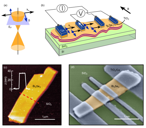
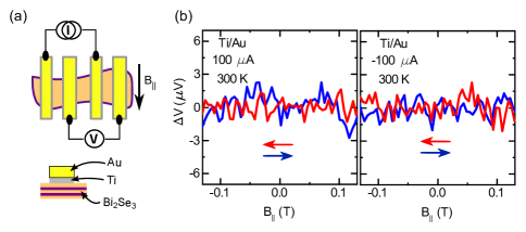
Here we demonstrate the room temperature electrical detection of spin polarized currents on the surface of the Bi2Se3. An applied electric field creates a finite momentum of the charge carriers yielding a perpendicularly locked spin transport on the surface, as depicted in Fig. 1a. We probe this current-induced spin polarization by using sensitive FM tunnel contacts (Fig. 1b) resulting in a spin-valve effect between the magnetization of the FM and the spin-polarized current on the Bi2Se3 surface. We used Bi2Se3 flakes mechanically exfoliated from single crystals onto a SiO2/Si substrate (Fig. 1c). The multi-terminal devices (Fig. 1d) with FM tunnel contacts of Co/TiO2 or standard contacts of Ti/Au were prepared by electron beam lithography (see Methods).
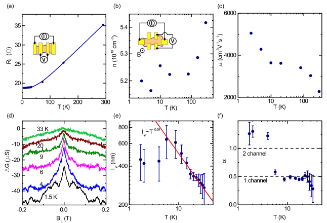
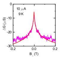
The Bi2Se3 flakes were characterized via electrical and magneto-transport measurements using Ti/Au contacts. The Bi2Se3 channel resistivity shows a metallic behaviour with a reduction in sheet resistance by a factor of two at low temperature (Fig. 2a). This stems from a large metallic charge carrier concentration of as extracted from Hall measurements (Fig. 2b). We observe a high channel mobility of at room temperature, which almost doubles at (Fig. 2c). These results imply a degenerate semiconducting behaviour with parallel surface and bulk conduction channels Butch2010 . Nevertheless, it has been demonstrated that the SML can still be probed despite a large bulk contributionLi2014b . Furthermore, the high mobility in our exfoliated flakes is promising for the detection of SML Butch2010 . These excellent properties are also reflected in the magneto-transport measurements, where we observed weak anti-localization (WAL) up to (Fig. 2d and supplementary Fig. S1) Hikami1980 . Topological insulators exhibit a very strong SO coupling and belong to the so-called symplectic class, where prefactor should be for one topological surface and for a bottom and top surfaceHe2011 . As shown in Fig. 2e, is found to be about 1.25 below and about at higher temperatures. This transition coincides with a phase coherence length at low temperatures and a dependence for higher temperatures (Fig. 2f). Both observations indicate that our samples are 2D systems with surface transport channels and large SO coupling He2011 ; Altshuler1982 . Such a large signature for WAL has been predicted to allow the direct detection of surface states by transport measurements at room temperatureHsieh2009 .
We focused on the detection of SML in the surface states of these Bi2Se3 flakes by FM tunnel contacts of Co/TiO2. The thin TiO2 layer at the interface introduces a contact resistance of preventing leakage current into the FM and protecting the SML by separating the Co and the Bi2Se3 surface states. Such contacts are known to be very sensitive to spin polarized currents up to room temperature, despite a background charge current Fert2008 ; Dash2009 .
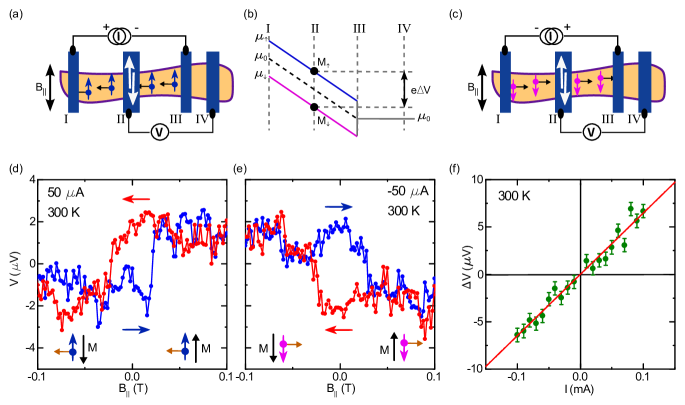
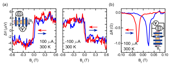
Figure 3a shows the measurement principle of our multi-terminal devices. The application of an electric bias between two contacts (I and III) results in a charge carrier flow with their spins locked perpendiculars to their momentum. This results in an spin polarized current on the surfaces of Bi2Se3. Another FM electrode (II) is used to probe the spin potentials in Bi2Se3 with respect to a reference contact (IV) outside the applied electric potential. If the spins on the Bi2Se3 and the FM magnetization are parallel, a larger potential drop can be detected than for the anti-parallel configuration (Fig. 3b). The magnetization of the FM detector can be switched by an in-plane magnetic field, whereas the spin orientation in Bi2Se3 can be flipped by inverting the current direction (Fig. 3c). Figure 3d shows the magnetic field dependence of the detected voltage signal at room temperature with a Bi2Se3 flake thickness of (Dev1). At a fixed applied bias current of we observe a change in voltage signal with the change in magnetization direction of the FM detector electrode. By sweeping the in-plane magnetic field we obtain a hysteretic spin signal which is an analogue of a spin-valve measurement. The switching field corresponds to the coercive field of our Co electrode as verified by anisotropic magnetoresistance measurements (see supplementary Fig. S3). The observed spin-valve signal is due to the projection of the spin polarized surface current, controlled by the current direction, on the magnetization of the FM detector, controlled by the external in-plane magnetic field. Reversing the current direction () locks the spins in the opposite direction resulting in an inverted hysteretic behaviour of the measured signal (Fig. 3e). A linear background was subtracted from the data due to the contribution from the charge electrochemical potential. A similar spin-valve behaviour has been measured at different bias currents at room temperature. We observe a point symmetry around zero bias and linear dependence of the spin signal (Fig. 3d), since the spin polarization is expected to be current independent and thus the spin density scales linearly with the current density Hong2012 .
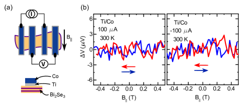
From the bias dependence and different control experiments at room temperature we can rule out any artefacts in the spin signals. The observed change in resistance implies that the signal originates from the SML in the TSS and not from Rashba SO coupling, which would exhibit the opposite sign Yazyev2010a . Any contribution of spin injections from other FM electrodes should be suppressed by the SML in the surface and the large SO coupling in the bulk states or would result in multiple switchings (suppelmentary Fig. S4). The linear bias dependence also rules out any heating related effects by the applied bias current, which should also be independent of the sign Dankert2013a . Furthermore, any localized Hall effects produced by fringe fields on the FM edges would be independent of the changes in magnetization and current direction Li2014b . Finally, we also rule out any similar contribution from Lorentz magnetoresistance of the Bi2Se3 channel and anisotropic ferromagnetic effect of the FMs by using control devices with non-magnetic Ti layer at the interface together with Co electrodes (Supplementary information S2). These control experiments unambiguously prove that the observed signals are due to the spin polarization in TI, which is detected by the FM tunnel contacts.
From the SML characteristics obtained in our devices, we can analytically evaluate the results to extract the spin polarization on the Bi2Se3 surface Hong2012 . The spin-valve signal , induced by a current , is directly related to the surface spin polarization :
where is the polarization of the FM detector and is the ballistic resistance Hong2012 . The ballistic conductance can be calculated by the conductance per channel times the number of channels , where is the width of our flake. The Fermi wave number can be derived from the charge carrier concentration, which we extracted from the Hall measurements Kittel2005 : Furthermore, we assume a maximum FM polarization for our Co/TiO2 contactsDankert2014a and a surface channel thickness of He2010 . Under these assumptions, we get a lower limit for the surface polarization . This is comparable to previous reports Li2014b and lies well within theoretical expectations, which predicted a limitation of the spin polarization up to 50% due to strong SO entanglement Yazyev2010a .
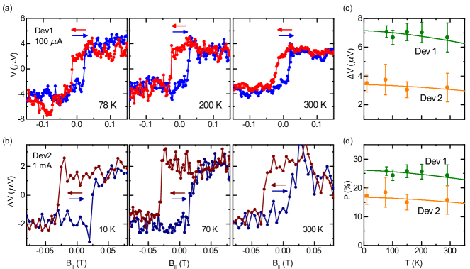
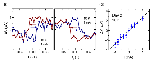
The measured spin valve signal is found to be very robust with temperature. Figure 4a shows the spin valve signals for Dev1 ( Bi2Se3) measured at different temperatures with a bias current of . The signals exhibit a clear switching and a signal amplitude of about . “Dev2” with Bi2Se3 shows a similar spin valve signal with an amplitude of about persistent up to room temperature, measured at a bias current of (Fig. 4b). The amplitude of both signals is almost independent of the temperature (Fig. 4c) and can be fitted with the theoretical model, , where is the Curie temperature of Co Shang1998 ; Dankert2013 . This implies that the signal amplitude depends only on the magnetization and thus spin polarization of the TiO2/Co tunnel contact, whereas no significant contribution stems from the Bi2Se3 surface polarization. Such a behaviour has been expected, since the surface states are thermally stable up to room temperature as shown by optical measurement techniques Hsieh2009 ; Hasan2010 . Assuming the bulk contribution increases proportionally with the number of quintuple layers Li2014b and taking the different flake geometries of both devices into account, we observe a scaling of the spin-resistance-area product for both of our devices. This is also reflected in the calculation of the spin polarization ranging from 17-26% (Fig. 4d). Such small deviations can also be due to differences in tunnel spin polarization of the FM tunnel contacts prepared in different runsDankert2014a . These results underline the reproducibility and implies that the signal originates from a spin polarization on the TI surface.
In summary, we have demonstrated the room temperature electrical detection of SML on the surface of thin exfoliated Bi2Se3 flakes by ferromagnetic tunnel contacts.A hysteretic spin valve signal could be observed reproducibly up to room temperature, with a lower limit of the surface spin polarization of 26%. It is expected that further control over the spin polarization can be achieved by accessing the dominant surface transport regime of the 3D TIs, for example by increasing the surface-to-volume ratio, compensation doping, or electric gating Hsieh2009 ; Hasan2010 . Positioning the Fermi level in the bandgap and controlling the surface carrier density will allow the electrical tuning of the spin polarization of the surface states Burkov2010 . Our results will pave the way for using TIs as spin polarized sources for spintronic devices at ambient temperatures. The possibility of coupling TIs to other materials for spin injection Modak2012 ; Kamalakar2014 opens up novel avenues in spintronic device design for energy efficient spin-logic applications in the future.
Methods
Fabrication The Bi2Se3 flakes were exfoliated from a bulk single crystal (from Cradley Crystals), using the conventional cleavage technique, onto a clean SiO2 ()/highly doped n-type Si substrate. The flakes were identified using a combination of optical and atomic-force microscopy (main Fig. 1c). We used multilayer Bi2Se3 with a thickness in the range of and widths of . Electrodes were patterned by electron beam lithography followed by contact deposition in an ultra-high vacuum electron beam evaporator. Electrodes with widths and channel length of are used. As contact material we used Ti/Au for the devices for Hall and WAL measurements, and TiO2/Co for the detection of spin-momentum locking. The TiO2 tunnel barrier for the latter was deposited by sputtering technique, using a DC Argon/Oxygen plasma with a Ti target.
Measurement The devices were measured with a Keithley 2400 Sourcemeter using direct current (DC). “Dev1” was measured in a liquid nitrogen cryostat between and . “Dev2” was measured in a liquid 4He cryostat with a temperature range of .
Acknowledgement The authors acknowledge the support of colleagues at the Quantum Device Physics Laboratory and Nanofabrication Laboratory at Chalmers University of Technology and thank Prof. Laurens W. Molenkamp for insightful discussions. This research is financially supported by the Nano Area of the Advance program at Chalmers University of Technology, EU FP7 Marie Curie Career Integration grant, the Swedish Research Council (VR) Young Researchers Grant and an EMM Nano Consortium scholarship.
Competing interests The authors declare no competing financial interests.
References
- (1) Xia, Y. et al. Observation of a large-gap topological-insulator class with a single Dirac cone on the surface. Nat. Phys. 5, 398–402 (2009).
- (2) Ando, Y. Topological Insulator Materials. J. Phys. Soc. Japan 82, 102001 (2013).
- (3) Hasan, M. Z. & Kane, C. Colloquium: topological insulators. Rev. Mod. Phys. 82, 3045 (2010).
- (4) Pesin, D. & MacDonald, A. H. Spintronics and pseudospintronics in graphene and topological insulators. Nat. Mater. 11, 409–16 (2012).
- (5) Zhang, H. et al. Topological insulators in Bi2Se3, Bi2Te3 and Sb2Te3 with a single Dirac cone on the surface. Nat. Phys. 5, 438–442 (2009).
- (6) Pan, Z.-H. et al. Electronic Structure of the Topological Insulator Bi2Se3 Using Angle-Resolved Photoemission Spectroscopy: Evidence for a Nearly Full Surface Spin Polarization. Phys. Rev. Lett. 106, 257004 (2011).
- (7) Hsieh, D. et al. A tunable topological insulator in the spin helical Dirac transport regime. Nature 460, 1101–5 (2009).
- (8) Pan, Z.-H. et al. Measurement of an Exceptionally Weak Electron-Phonon Coupling on the Surface of the Topological Insulator Bi2Se3 Using Angle-Resolved Photoemission Spectroscopy. Phys. Rev. Lett. 108, 187001 (2012).
- (9) König, M. et al. Quantum spin hall insulator state in HgTe quantum wells. Science 318, 766–70 (2007).
- (10) Brüne, C. et al. Evidence for the ballistic intrinsic spin Hall effect in HgTe nanostructures. Nat. Phys. 6, 448–454 (2010).
- (11) Mellnik, A. R. et al. Spin-transfer torque generated by a topological insulator. Nature 511, 449–451 (2014).
- (12) Shiomi, Y. et al. Bulk topological insulators as inborn spintronics detectors. arXiv:1312.7091 (2013).
- (13) Deorani, P. et al. Observation of inverse spin Hall effect in bismuth selenide. arXiv:1404.1146 (2014).
- (14) Li, C. et al. Electrical detection of charge-current-induced spin polarization due to spin-momentum locking in Bi2Se3. Nat. Nanotechnol. 9, 218–224 (2014).
- (15) Tian, J. et al. Topological insulator based spin valve devices: Evidence for spin polarized transport of spin-momentum-locked topological surface states. Solid State Commun. 191, 1–5 (2014).
- (16) Tang, J. et al. Electrical Detection of Spin-Polarized Surface States Conduction in (BiSb)2Te3 Topological Insulator. Nano Lett. 1–18 (2014).
- (17) Burkov, A. A. & Hawthorn, D. G. Spin and Charge Transport on the Surface of a Topological Insulator. Phys. Rev. Lett. 105, 066802 (2010).
- (18) Butch, N. P. et al. Strong surface scattering in ultrahigh-mobility Bi2Se3 topological insulator crystals. Phys. Rev. B 81, 241301 (2010).
- (19) Hikami, S., Larkin, A. & Nagaoka, Y. Spin-orbit interaction and magnetoresistance in the two dimensional random system. Prog. Theor. Phys. 63, 707–710 (1980).
- (20) He, H.-T. et al. Impurity Effect on Weak Antilocalization in the Topological Insulator Bi2Te3. Phys. Rev. Lett. 106, 166805 (2011).
- (21) Altshuler, B. L., Aronov, A. G. & Khmelnitsky, D. E. Effects of electron-electron collisions with small energy transfers on quantum localisation. J. Phys. C Solid State Phys. 15, 7367–7386 (1982).
- (22) Fert, A. Nobel Lecture: Origin, development, and future of spintronics. Rev. Mod. Phys. 80, 1517–1530 (2008).
- (23) Dash, S. P., Sharma, S., Patel, R. S., de Jong, M. P. & Jansen, R. Electrical Creation of Spin Polarization in Silicon at Room Temperature. Nature 462, 491–494 (2009).
- (24) Hong, S., Diep, V., Chen, Y. P. & Datta, S. Modeling potentiometric measurements in topological insulators including parallel channels. Phys. Rev. B 86, 085131 (2012).
- (25) Yazyev, O. V., Moore, J. E. & Louie, S. G. Spin Polarization and Transport of Surface States in the Topological Insulators Bi2Se3 and Bi2Te3 from First Principles. Phys. Rev. Lett. 105, 266806 (2010).
- (26) Dankert, A. & Dash, S. P. Thermal Creation of Electron Spin Polarization in n-Type Silicon. Appl. Phys. Lett. 103, 242405 (2013).
- (27) Kittel, C. & McEuen, P. Introduction to Solid State Physics, volume 10. John Wiley and Sons, 8 edition (2005).
- (28) Dankert, A., Mutta, V. K., Bergsten, J. & Dash, S. P. Spin transport and precession in graphene measured by nonlocal and three-terminal methods. Appl. Phys. Lett. 104, 192403 (2014).
- (29) He, K. et al. Crossover of the three-dimensional topological insulator Bi2Se3 to the two-dimensional limit. Nat. Phys. 6, 584–588 (2010).
- (30) Shang, C., Nowak, J., Jansen, R. & Moodera, J. S. Temperature dependence of magnetoresistance and surface magnetization in ferromagnetic tunnel junctions. Phys. Rev. B 58, R2917–R2920 (1998).
- (31) Dankert, A., Dulal, R. S. & Dash, S. P. Efficient Spin Injection into Silicon and the Role of the Schottky Barrier. Sci. Rep. 3, 3196 (2013).
- (32) Modak, S., Sengupta, K. & Sen, D. Spin injection into a metal from a topological insulator. Phys. Rev. B 86, 205114 (2012).
- (33) Kamalakar, M. V., Dankert, A., Bergsten, J., Ive, T. & Dash, S. P. Enhanced Tunnel Spin Injection into Graphene using Chemical Vapor Deposited Hexagonal Boron Nitride. Sci. Rep. 4, 6146 (2014).
- (34) Patel, R. S., Dash, S. P., de Jong, M. P. & Jansen, R. Magnetic tunnel contacts to silicon with low-work-function ytterbium nanolayers. J. Appl. Phys. 106, 016107 (2009).
- (35) Jansen, R., Min, B.-C. & Dash, S. P. Oscillatory spin-polarized tunnelling from silicon quantum wells controlled by electric field. Nat. Mater. 9, 133–8 (2010).
- (36) Tombros, N., Jozsa, C., Popinciuc, M., Jonkman, H. T. & van Wees, B. J. Electronic Spin Transport and Spin Precession in Single Graphene Layers at Room Temperature. Nature 448, 571–574 (2007).
- (37) Le Breton, J.-C., Sharma, S., Saito, H., Yuasa, S. & Jansen, R. Thermal spin current from a ferromagnet to silicon by Seebeck spin tunnelling. Nature 475, 82–5 (2011).
Supplementary information
Room
Temperature Electrical Detection of Spin Polarized Currents in Topological
Insulators
André Dankert
Johannes Geurs
M. Venkata Kamalakar
Saroj P. Dash
S1 Weak anti-localization measurement in Bi2Se3
Weak anti-localization is an interaction of an electron wave function in a material with a strong spin-orbit (SO) coupling. Without a SO interaction, a time-reversal pair of electron waves, scattered by impurities, interferes destructively (electron localization). This quantum interference occurs at the scale of the coherence length and yields a correction reducing the conductance around zero magnetic field. In comparison, a strong SO interaction enhances the conductance, which is known as the weak anti-localization (WAL) effect (Fig. S1). In the case of a 2D system, increasing an out-of-plane magnetic field breaks the time-reversal symmetry, which reduces gradually the conductance correction. This reduction can be explained by the Hikami-Larkin-Nagaoka (HLN) modelHikami1980 . In this model, the conductance correction is given by
| (1) |
where represents the digamma function, is the phase coherence length, and the prefactor describes the quantum systemHikami1980 . The decreasing peak size with increasing temperature is characteristic for WAL and we could observe a signal to a, for TIs unusually high, temperature of He2011 . Three-dimensional TIs with 2D surface states usually exhibit a very strong SO coupling and belong to the so-called symplectic class, where should be for one topological surface and for a bottom and top surfaceHe2011 . Figure S1 shows the WAL measurement at and the fitting with the HLN model, identical to the one in the main text.
S2 Control experiments with non-magnetic contacts
To demonstrate that the hysteretic switching, presented in the main paper, stems from a spin-valve effect between the current-induced spin polarization in the surface of the Bi2Se3 and the magnetization of the ferromagnetic (FM) contact, we prepared devices with non-magnetic Ti/Au electrodes (Fig. S2a) and with a non-magnetic Ti interlayer between Bi2Se3 and Co (Fig. S2a). This non-magnetic interlayer is known to suppress the spin polarization of the FM detector contact, while still keeping its magnetic propertiesPatel2009 ; Jansen2010a . The voltages detected by those nonmagnetic detector contacts exhibit no such field dependent switching, which rules out any other mechanisms,such as Lorentz magnetoresistance of the Bi2Se3 channel and anisotropic magnetoresistance (AMR) of the Co contacts (Fig. S2b) Dash2009 ; Dankert2013 .
S3 Influence of the multi-terminal configuration
We can also rule out any contribution of spin transport in the Bi2Se3 channel due to spin injection from the FM electrodes in our measured spin valves. Using a multi-terminal geometry could result in a similar signal, if the biasing FM electrodes induce a spin accumulation in the flake, which can be detected by the FM voltage probe. A single switch, as observed in our case, could be the result of an incomplete spin-valve measurement, similar to the ones in graphene Tombros2007 . Such an effect can be ruled out, since it would result in additional resistance changes when the injector contact magnetization is switching. The coercive field of the FM contacts we used should be in the range of . Sweeping the in-plane parallel field even to does only show the initially observed hysteretic switching (Fig. SS4a). Furthermore, this switching field correlates with the coercive field of the detector contact extracted from anisotropic magnetoresistance measurements (Fig. S4b). These observations are also supported by the theoretical expectations of a extremely short spin lifetime in the bulk and surface statesAndo2013a ; Hasan2010 . The strong spin-orbit coupling leads to a fast relaxation of any spin accumulation limiting the diffusion length to less than the distance between our electrodes. Therefore, only the spin polarization induced by the spin-momentum coupling on the surface can be detected. The origin of the spin accumulation in the surface is supported by the thickness dependence (see “Spin-momentum locking in thick Bi2Se3 (Dev2)”). Furthermore, control experiments with nonmagnetic contacts demonstrate the spin-related nature of the signal (see “Control experiment”).
S4 Spin-momentum locking in thick Bi2Se3 (Dev2)
As mentioned in the main text, the signal was reproduced in devices of different thicknesses. Dev1 had a thickness of about and exhibited a clear hysteretic switching with an amplitude of about at room temperature, using bias current. Dev2 had a thickness of about about resulting in signal amplitude using bias current at room temperature (Fig. SS5a). Such a behaviour is expected, since the bulk contribution increases with increasing number of quintuple layers resulting in a lower signal at the same current density Li2014b . Taking different contact areas into account, the scaling of the spin-resistance-area product should be . Regarding this, the signals measured in Dev2 scale accordingly and have a comparable temperature (see main Fig. 4) and bias dependence to the ones of Dev1 (Fig. S5b). The linear bias dependence of the spin signal and the sign change with bias current rule out signal due to thermal effects LeBreton2011a ; Dankert2013a .