Surface Plasmon Instability Leading to Emission of Radiation
Abstract
We propose a new energy conversion approach from a dc electric field to a terahertz wave based on hybrid semiconductors by combining two-dimensional (2D) crystalline layers and a thick conducting material with possible applications as a source of coherent radiation. The hybrid nano-structure may consist of a single or pair of sheets of graphene, silicene or a 2D electron gas as would occur at a semiconductor hetero-interface. When an electric current is passed through a layer, we discover that the low-frequency plasmons may become unstable beyond a critical wave vector . However, there is no instability for a single driven layer far from the conductor and the instability of an isolated pair of 2D layers occurs only at ultra long wavelengths. To bring in frequency agility for this spontaneous radiation, we manipulate the surface-plasmon induced instability, which leads to the emission of radiation (spiler), to occur at shorter wavelengths by choosing the conductor electron density, layer separation, distances of layers from the conductor surface and the driving-current strength. Applications of terahertz radiation from spiler for chemical analysis, security scanning, medical imaging and telecommunications are expected.
pacs:
73.21.-b, 71.70.Ej, 73.20.Mf, 71.45.Gm, 71.10.Ca, 81.05.uePossible sources of terahertz (THz) radiation have been investigated for several years now. These frequencies cover the electromagnetic (EM) spectrum lying between microwave and far-infrared. By epitaxially growing layers of different semiconductors (including GaAs, GaAs/AlGaAs, InAs/InGaAs), multiple quantum-well layers, which emit high-power THz radiation across a wide frequency range, have been fabricated. The work reported so far covers ultra-long wavelength emission, phase/mode-locking, multiple color generation, photonic crystal structures, and improved laser performance with respect to both maximum operating temperature and peak output power. It was predicted by Kempa, et al. Bakshi (see also Ref. [AI1, ]) that when a current is passed through a stationary electron gas, the Doppler shift in response frequency of this two-component plasma leads to a spontaneous generation of plasmon excitations at ultra-long wavelengths and subsequent Cherenkov radiation AI4star at sufficiently high carrier drift velocities. For their model, the process is irreversible based on the lack of time reversal symmetry (Onsager’s principle of microscopic reversibility) Onsager . Similar conclusions are expected for monolayer graphene which is characterized by massless Dirac fermions where the energy dispersion is linear in the wave vector or a nanosheet of silicene consisting of silicon atoms, which has been synthesized silicene . In the same group of the periodic table with graphene, silicene is predicted to exhibit similar electronic properties. Additionally, it has the advantage over graphene in its compatibility with Si-based device technologies.
The role played by plasma excitations in the THz response of low-dimensional microstructures has received considerable attention 4 ; 5 ; 6 ; 7 ; 8 ; 9 ; 10 ; 11 ; 12 ; 13 . Plasmon modes of quantum-well transistor structures with frequencies in the THz range may be excited with the use of far-infrared (FIR) radiation and other means Tso . A split grating gate design has been found to significantly enhance FIR response 2 ; 3 ; gg1 ; gg2 . Under this scheme, however, the stimulated EM radiation require either a population inversion laser or a quantum coherence LWI , or a condensation polar . The EM radiation can also be generated by transferring energy from optical field to another spaser .
Here, we explore a new energy conversion approach, i.e., from an applied dc electric field to an optical field based on a current-driven induced instability. The primary objective of the Letter is to expand the materials platform by exploiting the functionality of a composite nano-system consisting of a thick conductor (including a heavily-doped semiconductor) which is Coulomb coupled to 2D layered materials. The Coulomb coupling of the plasmons in a layer to the surface plasmon on the conductor results in a surface-plasmon instability that leads to the emission of radiation (spiler). The predicted tunable spiler radiation relies on a current-induced plasmon instability and comes after the plasmon grows in the time domain at a rate which is determined by the surface-plasmon frequency, the 2D layer separation, the distance of the 2D layers from the conducting surface and the driving-current strength.
In our formalism, we consider a nano-scale system consisting of a pair of 2D layers and a thick conducting material. The layer may be monolayer graphene or a 2DEG such as a semiconductor inversion layer or high electron mobility transistor. The graphene layer may have a gap, thereby extending the flexibility of the composite system that also incorporates a thick conducting layer.
In our notation, the structure has a double layer located at and () interacting with each other as well as the semi-infinite system with its surface lying in the -plane at . The longitudinal excitation spectra of allowable modes will be determined from a knowledge of the frequency-dependent non-local dielectric function which depends on the position coordinates , and frequency . Alternatively, the normal modes correspond to the resonances of the inverse dielectric function , satisfying . The significance of is that it embodies many-body effects AI2 through screening by the medium of an external potential to produce an effective potential . The self-consistent field equation for is in integral form, after Fourier transforming parallel to the -plane and suppressing the in-plane wave number and frequency , leading to
| (1) |
Here, the polarization function for the 2D structure is given by
| (2) |
where , , and the 2D response function obeys with as the single-particle in-plane response. Upon substituting this form of the polarization function for the monolayer into Eq. (1), we have
| (3) |
We now set and in turn in Eq. (3) and solve simultaneously the pair of equations for and to obtain
| (4) |
where with the coefficient matrix given by
| (7) |
In our numerical calculations, we shall use given in Eq. (30) of Ref. [Horing, ]. Substituting the results for and into Eq. (4), we obtain the complete inverse dielectric function for a pair of 2D conducting planes interacting with each other and a semi-infinite conducting material. The plasmon excitation frequencies are determined by the zeros of . Furthermore, the effect of the inverse dielectric function for the semi-infinite structure leads to coupling between the two layers and of each layer with the bulk and surface of the neighboring material. As a matter of fact, our result for the plasmon dispersion relation generalizes that obtained by Das Sarma and Madhukar DasSarma ; Ai3Pohl ; Polini for a biplane. We obtain in the local limit Horing
| (8) | |||||
Setting and letting in Eq. (7), the off-diagonal matrix elements tend to zero and the element in the first row and first column reduces to unity. Subsequently, the dispersion equation for a single layer interacting with the substrate is given by the zeros of the matrix element in the second row and second column. Using the long-wavelength limit (), we find . For a 2DEG, we have ; for doped graphene, we have , where is the chemical potential and is the gap between valence and conduction bands; for intrinsic graphene whose plasmon excitations are induced by temperature, SDSLi . Consequently, we find the plasmon frequency as follows NJMH : with and defined by and , where . Additionally, within this long-wavelength limit, these expressions yield the plasmon excitation frequencies and which are both linear in and unlike the -dependence for free-standing graphene or the 2DEG wunch ; pavlo ; 7+ ; 8+ ; 9+ ; 10+ .
In Ref. 1+ , it was demonstrated that the plasmon excitations in graphene has a linear dispersion rather than a square root dependence on the wave vector. This startling result came as a surprise because theoretical calculations on free-standing graphene clearly do not predict a linear dependence in the long-wavelength limit. As a matter of fact, this linear dependence of plasmon frequency on wave vector was attributed to local field corrections to the random-phase approximation. In our notation, for . The spectral function yields real frequencies. A plane interacting with the half-space has two resonant modes. Each pair of 2D layers interacting in isolation far from the semi-space medium supports a symmetric and an antisymmetric mode DasSarma . In the absence of a driving current, the analytic solutions for the plasmon modes of a pair of 2D layers that are Coulomb coupled to a half-space are given by
| (9) |
where and the term plays the role of “Rabi coupling”. Clearly, for long wavelengths, only depends on . However, the excitation spectrum changes dramatically when a current is driven through the configuration. Under a constant electric field, the carrier distribution is modified, as may be obtained by employing the relaxation-time approximation in the equation of motion for the center-of-mass momentum. For a parabolic energy band for carriers with effective mass and drift velocity determined by the electron mobility and the external electric field, the electrons in the medium are redistributed. This is determined by a momentum shift in the wave vector in the thermal-equilibrium energy distribution function . By making a change of variables in the well-known Lindhard polarization function , this effect is equivalent to a frequency shift . For massless Dirac fermions in graphene with linear energy dispersion, this Doppler shift in frequency is not in general valid for arbitrary wave vector. This is our conclusion after we relate the surface current density to the center-of-mass wave vector in a steady state. Our calculation shows that the redistribution of electrons leads to a shift in the wave vector appearing in the Fermi function by the center-of-mass wave vector , where and are the Fermi wave vector and velocity, respectively. However, in the long-wavelength limit, , the Doppler shift in frequency is approximately obeyed. Consequently, regardless of the nature of the 2D layer represented in the dispersion equation we may replace in the dispersion equation in the presence of an applied electric field at long wavelengths.
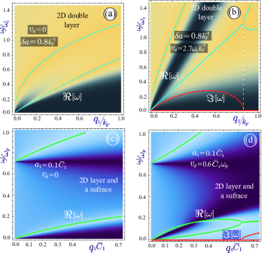
To highlight the effect due to a surface in spiler, as a comparison we first present in Figs. 1(a) and 1(b) the plasmon dispersion for an isolated pair of 2D layers in the absence DasSarma and presence Bakshi of a current, respectively. When a substrate surface plasmon is not contributing, the plasmon instability starts at and exists over a finite range until a bifurcation point is reached for . By going beyond this bifurcation point, the interlayer Coulomb coupling is effectively suppressed, leading to one uncoupled 2D-sheet plasma and two current-split 2D-sheet plasmon modes. However, when a surface plasmon interacts with the two 2D layers, the plasmon instability may be moved to shorter wavelengths, as we clearly illustrated in Figs. 1(d), where we show the results when spiler consists of a 2D layer and a semi-infinite conducting medium. Plasmon remains stable in a single current-driven 2D layer. In the presence of the surface plasmon, as in the plasmon instability occurs outside the closed Rabi “loop”, i.e., ( is the critical wave vector), and at shorter wavelengths by pushing significantly above zero.
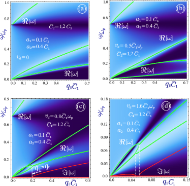
In order to get a full understanding of the mechanism for instability shown in Fig. 1, in Fig. 2 we have numerically investigated the effect of a passing current through a layer of 2DEG, graphene or silicene which is Coulomb coupled to a conductor. Specifically, we consider a pair of 2D layers and a semi-infinite medium such as a heavily-doped semiconductor. We present in Fig. 2 both the plasmon dispersion and the inverse growth rate. Each panel shows results for a different drift velocity given by and . In the absence of a current, panel shows that there are three plasmon excitation branches, which are stable as given by Eq. (Surface Plasmon Instability Leading to Emission of Radiation). At low , panel demonstrates that the plasmons are still stable. However, as is increased further, the lowest branches may become unstable as in and through the appearance of a positive imaginary part for the frequency. There is a threshold value for beyond which the plasmon excitation becomes unstable. On the other hand, the existence of the surface plasmon greatly screens both the interlayer and intralayer Coulomb couplings as in the range of . This stabilizes the plasmon excitation for by suppressing the interlayer coupling as shown in . As increases to in , reduces almost to zero, but the wide stable region in is squeezed into a narrow belt. The occurrence of such a new unstable region starting from is a combined result from both the surface-induced softening of the two 2D-sheet plasma modes to two acoustic-like plasmon modes as well as the strong interlayer coupling for small layer separation. To some extent, this feature is similar to the result displayed in Fig. 1 for the isolated pair of 2D layers.
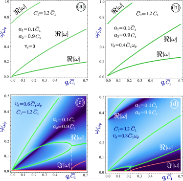
Figure 3 illustrates our results for larger 2D layer separations from each other compared to the case in Fig. 2. Panel again corresponds to the analytic solutions in Eq. (Surface Plasmon Instability Leading to Emission of Radiation) when . The plasmon excitations are all still stable in at . However, as is increased further in and , an instability appears at , which is exactly where the Rabi “loop” for plasmon excitations closes in the two lower panels. Beyond , the plasmon becomes unstable corresponding to opposite phase velocities for two current-split plasmon branches. The loop shape is quite different for current passing through the 2D layer [in ] and the semi-infinite medium [in ]. We also note that by adjusting the layer separation, we may change value for controlling the onset of the plasmon instability. With such a large interlayer separation, the interlayer interaction becomes very weak and the system effectively behaves like the single current-driven 2D layer coupled to a conducting surface, similar to that in Figs. 1.
Physically, from the point of view of momentum space, electrons may only occupy momentum space within the range of at zero temperature in a state of thermal equilibrium, where is the electron Fermi wave number and is the Fermi energy. When a current is passed through the electron gas, electrons are driven out from this thermal-equilibrium state and their population becomes asymmetrical with respect to . In this case, the Fermi energy is split into and with , where represents the electron center-of-mass momentum. In this shifted Fermi-Dirac distribution model, electrons in such a non-equilibrium state are energetically unstable, and the higher-energy electrons in the range tend to decay into lower-energy empty states by emitting EM waves and phonons to ensure the conservations of total momentum and energy.
The current-driven asymmetric electron distribution in space leads to an induced oscillating polarization current or a “dipole radiator”. If two electron gas layers are placed close enough, the in-phase interlayer Coulomb interaction will give rise to a dipole-like plasmon excitation, similar to that of a single layer. On the other hand, the out-of-phase interlayer Coulomb coupling will lead to a quadruple-like excitation. This quadruple-like plasmon excitation can be effectively converted into a transverse EM field in free space if a surface grating is employed.
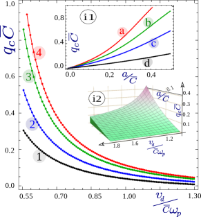
The surface-induced instability in spiler may lead to EM radiation, and the lower edge of its radiation frequency can be tuned directly by to cover the THz frequency range. Here, we present in Fig. 4 the dependence of controlling parameter as functions of and separation for a single 2D layer coupled to surface plasmon, where is increased with either reducing or increasing . These results clearly demonstrate significant shifts of within the desired ranges for operations of both photodetectors and EM-wave devices.
In summary, we are proposing a spiler quantum plasmonic device which employs 2D layers such as graphene/III-V semiconductor hybrids in combination with a thick conducting material with clean interfaces. We find that the spiler spontaneously emits EM radiation when a current is passed through the 2D layer or the underlying conductor to make the plasmons become unstable at a specific frequency and wave number. It is possible to tune the onset of plasmon instability by selecting the properties of the nanosheet or frequency of the surface plasmon, i.e., the substrate. The surface plasmon plays a crucial role in giving rise to the splitting and the concomitant streams of quasiparticles whose phase velocities are in opposite directions when the instability takes place. The emitted EM radiation may be coupled easily outward to a free space by a grating on the surface. Finally, we note that in presenting our numerical results, we measured frequency in terms of the bulk plasmon frequency which, typically for conductors, is eV. Either for intrinsic graphene, doped monolayer graphene or an inversion layer 2DEG, we have m and m/s. The frequency unit used in Fig. 1 is which is of the same order as .
Experimentally, the emitted EM radiation of a spiler device can be detected by heterodyne mixing technique using a planar Schottky diode reno . In this experiment, the mixing of the EM radiation against a molecular laser line is known to give a high precision measurement of the EM radiation frequency and can also show transient turn-on behavior in a pulsed spiler device.
The spontaneous EM radiation from the proposed spiler does not require a population inversion in a laser, a coupling-field quantum coherence in amplification without inversion and a exciton-polariton condensation laser ; LWI ; polar . Instead, it depends on energy conversion spaser from an applied dc electric field to an optical field based on a current-induced plasmon instability. The radiation frequency of the splier is tunable and covers the whole THz range. Terahertz waves are able to penetrate materials that block visible light and have a wide range of possible applications, including chemical analysis, security scanning, medical imaging, and telecommunications.
Acknowledgements.
This research was supported by contract # FA 9453-13-1-0291 of AFRL. DH would like to thank the Air Force Office of Scientific Research (AFOSR) for its support. We thank Oleksiy Roslyak and Antonios Balassis for helpful discussions. WP was supported by the U.S. Department of Energy, Office of Science, Basic Energy Sciences, Materials Sciences and Engineering Division.References
- (1) K. Kempa, P. Bakshi, J. Cen, and H. Xie, Phys. Rev. B43, 9273 (1991).
- (2) S. Tariq, A. M. Mirza, and W. Masood, Phys. Plasmas 17, 102705 (2010).
- (3) M. Akbari-Moghanjoughi, Phys. Plasmas 21, 053301 (2014).
- (4) L. Onsager, Phys. Rev. 37, 405 (1931).
- (5) C.-C. Liu, W. Feng, and Y. Yao, Phys. Rev. Lett. 107, 076802 (2011).
- (6) S. J. Allen, D. S. Tsui, and R. A. Logan, Phys. Rev. Lett. 38, 980 (1977).
- (7) D. S. Tsui, S. J. Allen, R. A. Logan, A. Kamgar, and S. N. Coopersmith, Surf. Sci. 73, 419 (1978).
- (8) S. Katayama, J. Phys. Soc. Japan 60, 1123 (1991); Surf. Sci. 263, 359 (1992).
- (9) C. Steinebach, D. Heitmann, and V. Gudmundsson, Phys. Rev. B56, 6742 (1997).
- (10) B. P. van Zyl and E. Zaremba, Phys. Rev. B59, 2079 (1999).
- (11) S. A. Mikhailov, Phys. Rev. B58, 1517 (1998).
- (12) O. R. Matov, O. F. Meshkov, and, V. V. Popov, JETP 86, 538 (1998).
- (13) O. R. Matov, O. V. Polischuk, and V. V. Popov, JETP 95, 505 (2002).
- (14) G, Gumbs and D. H. Huang, Phys. Rev. B75, 115314 (2007).
- (15) D. H. Huang, G. Gumbs, P. M. Alsing, and D. A. Cardimona, Phys. Rev. B77, 165404 (2008).
- (16) N. J. M. Horing, H. C. Tso, and G. Gumbs, Phys. Rev. B36, 1588 (1987).
- (17) E. A. Shaner, A. D. Grine, M. C. Wanke, Mark Lee, J. L. Reno, and S. J. Allen, IEEE Photon. Technol. Lett. 18, 1925 (2006).
- (18) V. V. Popov, T. V. Teperik, G. M. Tsymbalov, X. G. Peralta, S. J. Allen, N. J. M. Horing, and M. C. Wanke, Semicond. Sci. Technol. 19, S71 (2004).
- (19) A. Balassis and G. Gumbs, J. Appl. Phys. 106, 103102 (2009).
- (20) A. Balassis, G. Gumbs, and D. H. Huang, Proc. SPIE 7467, 74670O (2009).
- (21) A. L. Schawlow and C. H. Townes, Phys. Rev. 112, 1940 (1958).
- (22) H. Fearn, C. Keitel, M. O. Scully, and S. Y. Zhu, Opt. Commun. 87, 323 (1992).
- (23) S. Christopoulos, G. B. H. von Högersthal, A. J. D. Grundy, P. G. Lagoudakis, A.V. Kavokin, J. J. Baumberg, G. Christmann, R. Butté, E. Feltin, J.-F. Carlin, and N. Grandjean, Phys. Rev. Lett. 98, 126405 (2007).
- (24) D. J. Bergman and M. I. Stockman, Phys. Rev. Lett. 90, 027402 (2003).
- (25) K. A. Kouzakov and J. Berakdar, Phys. Rev. A85, 022901 (2012).
- (26) N. J. M. Horing, E. Kamen, and H.-L. Cui, Phys. Rev. B32, 2184 (1985).
- (27) S. Das Sarma and A. Madhukar, Phys. Rev. B23, 805 (1981).
- (28) K. Pohl, B. Diaconescu, G. Vercelli, L. Vattuone, V. M. Silkin, E. V. Chulkov, P. M. Echenique, and M. Rocca, Europhys. Lett. 90, 57006 (2010).
- (29) R. E. V. Profumo, R. Asgari, M. Polini, and A. H. MacDonald, Phys. Rev. B85 085443 (2012).
- (30) S. Das Sarma and Q. Li, Phys. Rev. B87, 235418 (2014).
- (31) N. J. M. Horing, Phys. Rev. B80, 193401 (2009).
- (32) B. Wunsch, T. Stauber, F. Sols, and F. Guinea, New J. Phys. 8, 318 (2006).
- (33) P. K. Pyatkovskiy, J. Phys.: Condens. Matt. 21, 025506 (2009).
- (34) K. W.-K. Shung, Phys. Rev. B34, 979 (1986).
- (35) K. W.-K. Shung, Phys. Rev. B34, 1264 (1986).
- (36) T. Ando, J. Phys. Soc. Jpn. 75, 074716 (2006).
- (37) E. H. Hwang and S. Das Sarma, Phys. Rev. B75, 205418 (2007).
- (38) C. Kramberger, R. Hambach, C. Giorgetti, M. H. Rümmeli, M. Knupfer, J. Fink, B. Büchner, L. Reining, E. Einarsson, S. Maruyama, F. Sottile, K. Hannewald, V. Olevano, A. G. Marinopoulos, and T. Pichler, Phys. Rev. Lett. 100, 196803 (2008).
- (39) M. Lee, M. C. Wanke, M. Lerttamrab, E. W. Young, A. D. Grine, J. L. Reno, P. H. Siegel, and R. J. Dengler, IEEE J. Selected Topics Quantum Electr. 14, 370 (2008).