Topological Modes in One Dimensional Solids and Photonic Crystals
Abstract
It is shown theoretically that a one-dimensional crystal with time reversal symmetry is characterized by a topological invariant that predicts the existence or otherwise of edge states. This is confirmed experimentally through the construction and simulation of a photonic crystal analogue in the microwave regime.
Topological phases have been shown to arise in a number of condensed matter systems: in the quantum Hall effectThouless et al. (1982) where electrons are confined to two dimensions and subject to a perpendicular applied magnetic field and in so-called topological insulatorsHasan and Kane (2010); Qi and Zhang (2011) which are materials the possess conducting metallic surfaces despite being insulators in the bulk. Experimental studies of these states, in materials such as grapheneCastro Neto et al. (2009) and Bi2Se3 have recently been an area of considerable focus both for fundamental reasons, because the topological states in these materials lead to exotic quasi-particles, and also for applications such as quantum computing.
The states arise in these systems as follows: consider a map from the Brillouin zone to a space of nondegenerate Bloch Hamiltonians . If is an eigenstate of , then a vector potential may be defined following BerryBerry (1984). The topological index of this map called the Chern number is . Thouless et al. discovered that non-trivial Chern numbers can arise in the Brillouin zone with time reversal symmetry broken by the application of a strong magnetic field as in the quantum Hall effectThouless et al. (1982). More recently Balents and MooreMoore and Balents (2007) applied this paradigm to systems with strong spin-orbit interaction but with time reversal symmetry intact and thereby clarified an earlier proposition by Kane and MeleKane and Mele (2005) that a invariant of the band structure divides insulators into two classes: an even class corresponding to conventional insulators and an odd topological insulating phase that possesses conductive surface states. Both spin-orbit coupling and breaking of inversion symmetry are prerequisites for such materials.
In this paper, we apply this paradigm to a system with different symmetry, a one-dimensional crystal with time reversal and charge conjugation symmetry. In the language of random matrix theoryAltland and Zirnbauer (1997), our system corresponds to class BDI in contrast to the unitary class A in the work of Thouless et al.Thouless et al. (1982) and the symplectic class AII in Balents and MooreMoore and Balents (2007). By an analogous argument, it is shown that such a structure may possess edge states characterized by a topological invariant. The system is then realized experimentally through a photonic analogue. We stress that while edge states such as Tamm states are well known in 1D crystalstuan Fang et al. (2013), it is the topologically-protected nature of those presented here that primarily concerns us.
Model—We begin with the topological argument. Consider a tight binding model on a one dimensional-lattice with nearest neighbor hopping and a constant on-site energy. Such a model is described by the following Schrödinger equation,
| (1) |
where as usual the represent the amplitude of the wavefunction at the -th lattice site and is the real hopping coefficient between the -th site to the th site. As is well-known, for arbitrary , the model (1) possesses a time-reversal symmetry with associated operator,
| (2) |
as well as a particle-hole symmetry represented by the anti-unitary charge conjugation operator,
| (3) |
and where,
| (4) |
The particle-hole symmetry restricts the Hamiltonian’s spectrum because if is an eigenfunction of (1) with energy , then is also an eigenfunction with energy .
For simplicity, a bi-partite lattice is now considered where the bond strengths are alternately and . The Schrödinger equation for this situation has the form
| (5) |
This may be diagonalized by introducing the Bloch ansatz, , yielding,
| (6) |
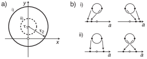
where the matrix on the left of eq (6) is the Bloch Hamiltonian, and . Eq (6) thus defines a map from the Brillouin zone to the space of Bloch Hamiltonians. Equivalently, this may be viewed as a map from a unit circle in the plane (the Brillouin zone) to the complex plane with the origin excluded. The origin is excluded provided, as we assume, the bands are non-degenerate. The homotopy of the punctured plane is well known to be non-trivial. The Chern number in this case corresponds to the number of times the loop winds about the origin. It is easy to see that for the case , [fig. 1(a)(i)]; for , [fig. 1(a)(ii)]. This can also be determined more formally by constructing the eigenspinors of the Bloch Hamiltonian, computing the corresponding Berry connection, and evaluating the Wilson loop . We will explain below why higher values of cannot be obtained even if we perturb the model (e.g. by incorporating longer range hopping that respects and symmetry).
It is straightforward to verify that the Chern number is associated with a zero energy bound state by noting that if the lattice is curtailed, so that represents the leftmost edge, the wave function will obey the boundary condition
| (7) |
Setting it follows that the solution to eqs (5) and (7) is
| (8) |
which is finite as only if , and in such a case is manifestly localized in character.
Now let us reformulate the argument with more generality. We continue to assume that the crystal has a bi-partite lattice and that the Hamiltonian commutes with and anti-commutes with . and transform a plane wave of wave vector into one of wave-vector . At the same time the amplitudes are transformed to and respectively. The two symmetries relate the Bloch Hamiltonians at wave-vectors and via . Together these relations and the requirement of hermiticity constrain the Bloch Hamiltonian to be off-diagonal. At the special points and which are invariant under the Bloch Hamiltonian is required to have the form
| (9) |
Here is real and since we are assuming that the bands have no accidental degeneracies. Topologically, this space is a punctured line. Rather than considering the mapping of the entire Brillouin zone to the space of Bloch Hamiltonians as before we may instead consider the mapping from the two special points and to the punctured line. Such maps fall into two classes: a trivial one [fig. 1(b)(i)] where the special points are mapped to the same side of the origin, , and a non-trivial case [fig. 1(b)(ii)] such that the special points are mapped to opposite sides111If we assume that for generic values of the Bloch Hamiltonian will not accidentally have the form eq (9) then the map from the Brillouin zone to the complex plane can cross the axis only at and ; this is the reason that the winding number can only equal or .. The edge mode occurs in the non-trivial case.
Our argument mirrors that of Balents and MooreMoore and Balents (2007) who considered maps from an effective Brillouin zone in two dimensions which had the topology of a cylinder to the space of Bloch Hamiltonians. The circular boundaries of the effective Brillouin zone in their argument are analogous to our special points and . Apart from the difference in dimensionality another key difference between their work and ours is in the symmetry. As noted above they considered bands with odd time reversal symmetry (the symplectic class AII) whereas we consider even time reversal symmetry accompanied by charge conjugation symmetry (class BDI). As a consequence breaking of spatial inversion symmetry is essential for non-trivial topology in their analysis but not for the class of topological insulator considered here. Indeed the model eq (1) respects parity.
We now address the issue of how the edge state might be observed. The hopping model on a bipartite lattice is actualized in a 1D solid where an electron is subject to a periodic array of potential barriers of alternating height. The reflection and transmission of incident free particle wavefunctions of wavevector through such a structure is readily determined by matching local solutions to the Schrödinger equation at interfaces using matrix methodsSprung and Morozov (2007). To do so, define,
| (10) |
Here is the transfer matrix for a single symmetric barrier located at the origin and a translation operator; is the opacity of the barrier, is the lattice spacing. In the limit of large barriers, where is the barrier width and is an overall phase shift.
The band structure of the bipartite lattice, with alternating barriers of opacity and respectively, is determined by finding the eigenvalues of the transfer matrix corresponding to the unit cell, i.e. . For , the usual band, i.e. values of such that the eigenvalues are complex, is found to split into two sub-bands symmetrically placed around the point and with edges corresponding to the roots of . Between these subbands, including the point , the reflection coefficient ; the phase shift of a reflected wave, however, experiences a jump of around if and otherwise. The jump leads to a Lorentzian feature in the time delay of a reflected wave; the width was determined by routine calculations to be,
| (11) |
Hence, the topological mode may be observed experimentally by a technique such as Time Delay Reflection Spectroscopy. As will be seen shortly, for a finite structure evidence of the topological mode is also available in some circumstances from the reflection profile.
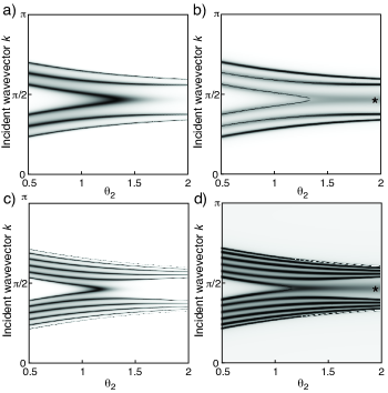
To verify the above arguments, we numerically evaluated the reflection coefficient and time delay for a 3.5 period structure from the transfer matrix as a function of and with fixed , , . Results are plotted in fig. 3. When the reflection spectrum [fig. 3(a)] consists of 6 minima, which correspond to a band in a structure with an infinite number of unit cells. As is increased, the central two minima move closer together and merge around ; as , this mid-band mode vanishes in reflection, contributing only a phase shift to the reflected light as discussed earlier. Conversely, if , the central minima become separated and, as predicted by the topological argument above, no mid-band mode exists. Results for 6.5 units are shown in fig. 3(c) and (d); the additional layers generate corresponding modes, but the topological mode remains for . If the number of periods is increased further, more modes appear to eventually yield the two sub-bands of the infinite bipartite lattice and the mid-gap mode persists confirming its topological nature.
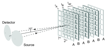
Photonic analogue— In order to conveniently verify the veracity of the topological index as a predictor of edge states, we exploit the known isomorphism between the Schrödinger equation and Maxwell’s equations in one dimensionHooper et al. (2006) to construct a photonic analogue structure in the microwave regime.
The experimental setup is illustrated in fig. 2 and details of the data collection described more fully in Butler (2012). The experimental structure itself consists of alternating layers of dielectric (air) and metamaterials. The metamaterial layers are separated by metallic spacers around the edge of the sample yielding a nominal spacing of . The metamaterial layers are made from a solid aluminium sheet perforated with a periodic square array of holes of pitch and hole size of ; the thickness of the metamaterial in successive layers is alternated, and denoted and respectively, to form the required ABAB bipartite stack with 3.5 unit cells as modelled earlier. When illuminated with microwave radiation between and GHz, the metamaterial supports only evanescently decaying modes in the subwavelength holes; hence the metamaterial layer behaves as an effective metal layer McCalmont et al. (1996) with a skin depth of . This arrangement is used rather than homogenous metal plates because metals behave as near perfect electrical conductors at microwave frequencies; thin metallic films could be used but by using a metamaterial the resulting structure is less sensitive to variations in thickness. The effective properties of the metamaterial layer can also be controlled much more precisely by adjusting the design parameters i.e. thickness, pitch and fill fraction.
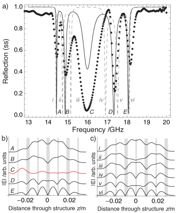
In the experiment, the sample is illuminated by a collimated -polarized (transverse electric) microwave beam, produced by a microwave horn placed at the focus of a spherical mirror, incident on the sample at Reflected intensity is measured as a function of frequency using a detector horn and secondary mirror. The sample studied had , specifically and as measured from the constructed sample. Since the opacity parameters of eq. (10) monotonically increase with the thicknesses , the topological argument above predicts that the edge states should be observed in this case. The reflected intensity is plotted as a function of frequency in fig. 4(a), confirming the presence of the midgap topological mode. Due to the finite number of periods in the structure, the band is manifested as a series of reflection minima corresponding to resonant modes in the structure; if the number of unit cells were increased, the continuous sub-bands would be recoveredGriffiths and Steinke (2001). We also simulated the response of a reversed structure, i.e. where and ; the reflection profile is plotted in gray in fig. 4(a). No mid-gap topological mode is observed in this structure in agreement with the above prediction.
To characterize the nature of these modes, we numerically modelled the reflection response of the structures using commercial finite-element software (Comsol). As with other experimentsButler et al. (2009, 2011), modelling can be used to visualize the electric field distribution in each mode. The simulated response is plotted in fig. 4(a). We emphasize that no fitting was performed and the agreement between model and data displayed in fig. 4(a) is typical for such studies, accurately locating the position of the minima while incorrectly estimating their depth. This discrepency is due to a number of physical effects including: finite area of the sample in the experiment; spherical aberration of the microwave source and detector; imperfections in the experimental sample such as bowing of the metamaterial layers which changes the dielectric spacing; and a radius of curvature associated with the hole edges that reduces the effective skin depth.
Plots of the time averaged electric field magnitude as a function of the distance through the sample are displayed in fig. 4(b) for each reflection minimum in the fitted profile fig. 4(a). Modes A,B,D and E are clearly distinct in character from mode C. Mode C has the predicted properties of the topological edge state: it is confined to the edge of the sample and also occurs in the middle of the band. Plots of the average electric field are also shown in fig. 4(c) for the six minima in the reversed structure. Unlike the previous case, none of the modes i—vi are localized to the edges, in agreement with the prediction of the above topological argument.
Conclusion—A topologically protected edge state has been experimentally observed in a 1D photonic crystal with time-reversal symmetry. The existence or otherwise of the state as a function of the design parameters of the crystal is predicted by a topological invariant that classifies mappings from the band structure to the space of Bloch Hamiltonians; the classification was constructed using methods previously applied to two and three dimensional topological insulators. However the crystals we consider are of a different class from conventional topological insulators in terms of their symmetries. The latter must have time reversal symmetry, strong spin-orbit interaction and a lack of inversion symmetry; in our work we use an anti-unitary charge conjugation symmetry as well as the time-reversal operator to develop the classification.
Acknowledgement—The authors wish to acknowledge financial support from the EPSRC through the QUEST programme grant (EP/I034548/1) and also QinetiQ and the EPSRC for funding CAMB through the Industrial CASE scheme (no. 08000346). HM is supported by a grant from the U.S. Department of Energy to the Particle Astrophysics Theory group at CWRU.
References
- Thouless et al. (1982) D. J. Thouless, M. Kohmoto, M. P. Nightingale, and M. den Nijs, Phys. Rev. Lett. 49, 405 (1982).
- Hasan and Kane (2010) M. Z. Hasan and C. L. Kane, Rev. Mod. Phys. 82, 3045 (2010).
- Qi and Zhang (2011) X.-L. Qi and S.-C. Zhang, Rev. Mod. Phys. 83, 1057 (2011).
- Castro Neto et al. (2009) A. H. Castro Neto, F. Guinea, N. M. R. Peres, K. S. Novoselov, and A. K. Geim, Rev. Mod. Phys. 81, 109 (2009).
- Berry (1984) M. V. Berry, Proc. Roy. Soc. A 392, 45 (1984).
- Moore and Balents (2007) J. E. Moore and L. Balents, Phys. Rev. B 75, 121306 (2007).
- Kane and Mele (2005) C. L. Kane and E. J. Mele, Phys. Rev. Lett. 95, 146802 (2005).
- Altland and Zirnbauer (1997) A. Altland and M. R. Zirnbauer, Phys. Rev. B 55, 1142 (1997).
- tuan Fang et al. (2013) Y. tuan Fang, L. kun Chen, N. Zhu, and J. Zhou, Optoelectronics, IET 7, 9 (2013).
- Sprung and Morozov (2007) D. Sprung and G. Morozov, Journal of Physics A (2007).
- Hooper et al. (2006) I. R. Hooper, T. W. Preist, and J. R. Sambles, Phys. Rev. Lett. 97, 053902 (2006).
- Butler (2012) C. Butler, The Microwave Response of Square Mesh Metamaterials, Ph.D. thesis, University of Exeter (2012).
- McCalmont et al. (1996) J. S. McCalmont, M. M. Sigalas, G. Tuttle, K. Ho, and C. M. Soukolis, Appl. Phys. Lett. 68 (1996).
- Griffiths and Steinke (2001) D. Griffiths and C. Steinke, Am. J. Phys. 69, 137 (2001).
- Butler et al. (2009) C. A. M. Butler, J. Parsons, J. R. Sambles, A. P. Hibbins, and P. A. Hobson, Appl. Phys. Lett. 95, 174101 (2009).
- Butler et al. (2011) C. A. M. Butler, I. R. Hooper, A. P. Hibbins, J. R. Sambles, and P. A. Hobson, J. Appl. Phys. 109, 013104 (2011).