Envelope function method for electrons in slowly-varying inhomogeneously deformed crystals
Abstract
We develop a new envelope-function formalism to describe electrons in slowly-varying inhomogeneously strained semiconductor crystals. A coordinate transformation is used to map a deformed crystal back to geometrically undeformed structure with deformed crystal potential. The single-particle Schrödinger equation is solved in the undeformed coordinates using envelope function expansion, wherein electronic wavefunctions are written in terms of strain-parametrized Bloch functions modulated by slowly varying envelope functions. Adopting local approximation of electronic structure, the unknown crystal potential in Schrödinger equation can be replaced by the strain-parametrized Bloch functions and the associated strain-parametrized energy eigenvalues, which can be constructed from unit-cell level ab initio or semi-empirical calculations of homogeneously deformed crystals at a chosen crystal momentum. The Schrödinger equation is then transformed into a coupled differential equation for the envelope functions and solved as a generalized matrix eigenvector problem. As the envelope functions are slowly varying, coarse spatial or Fourier grid can be used to represent the envelope functions, enabling the method to treat relatively large systems. We demonstrate the effectiveness of this method using a one-dimensional model, where we show that the method can achieve high accuracy in the calculation of energy eigenstates with relatively low cost compared to direct diagonalization of Hamiltonian. We further derive envelope function equations that allow the method to be used empirically, in which case certain parameters in the envelope function equations will be fitted to experimental data.
I Introduction
It has long been recognized that elastic strain can be used to tune the properties of materials. This idea of elastic strain engineering (ESE) is straightforward because the derivative of a material property with respect to applied elastic strain , , is in-general non-zero.Li et al. (2014) However, ESE has traditionally been limited by the small amount of elastic strain a material can accommodate, before plastic deformation or fracture occurs. Recent experiments, however, reveal a class of ultra-strength materialsLi et al. (2014) whose elastic strain limit can be significantly higher than conventional bulk solids. Notable examples are two-dimensional (2D) atomic crystals such as graphene and monolayer molybdenum disulfide (MoS2).Novoselov et al. (2005) The experimentally measured elastic strain limit of graphene can be as high as 25%,Lee et al. (2008); Liu et al. (2007) while that of bulk graphite seldom reaches 0.1%. Monolayer MoS2 can also sustain effective in-plane strain up to 11%.Bertolazzi et al. (2011) Such large elastic strain limit make it possible to induce significant material property changes through the application of elastic strain. In particular, position-dependent properties can be induced by applying inhomogeneous strain which is slowly varying at atomic scale but has large sample-wide difference. For instance, Feng et al demonstrated that indenting a suspended MoS2 monolayer can create a local electronic bandgap profile in the monolayer with spatial variation, being the distance to the center of indenter tip.Feng et al. (2012) This creates an “artificial atom” in which electrons moves in a semiclassical potential resembling that of a two-dimensional hydrogenic atom. In this article, we will develop a new envelope function formalism that could be used to study the electronic structure of such slowly-varying inhomogeneously strained crystals.
Ab initio electronic structure methods such as density functional theory (DFT) are nowadays routinely used to calculate the properties of materials. However, the steep scaling of computational cost with respect to system size limits their use to periodic solids, surfaces and small clusters. An inhomogeneously strained structure usually involves a large number of atoms and thus fall beyond the current capabilities of these methods.
In the past, several semi-empirical electronic structure methods capable of treating systems larger than ab initio methods have been developed to study the electrical and optical properties of semiconductor nanostructures. Among those the most notable are the empirical tight binding method, Slater and Koster (1954); Di Carlo (2003) empirical pseudopotential method (EPM) Zunger (1998); Canning et al. (2000); Wang and Zunger (1999) and multi-band envelope function method. Luttinger and Kohn (1955); Bastard (1981); Baraff and Gershoni (1991); Gershoni et al. (1993); Burt (1992, 1999) Both tight-binding and EPM are microscopic methods Di Carlo (2003) that treat the electronic structure at the level of atoms, while the multi-band envelope function method describes electronic structure at the level of the envelope of wavefunctions, whose lengthscale is in general much larger than the lattice constant. Excellent articles discussing the merits and shortcomings of these methods exist in the literature. Di Carlo (2003); Zunger (1998) Below we shall briefly review the multi-band envelope function method and the EPM method, as these two methods have been demonstrated to treat vary large nanostructures (up to a million atoms Wang and Zunger (1996, 1999)) and are most relevant to our article.
The starting point of wavefunction based semi-empirical electronic structure methods is usually the single-particle Schrödinger equation:
| (1) |
Here is the crystal potential; is the electronic wavefunction. In envelope function method, is expanded in terms of a complete and orthonormal basis set , Luttinger and Kohn (1955) where represent the Bloch functions of the underlying periodic solid at a reference crystal momentum . Mathematically, the expansion is written as
| (2) |
The summation is over band index and wave vector , which is restricted to the first Brillouin zone (BZ) of the crystal. This expansion can be re-written as
| (3) |
The functions are called envelope functions because they are smooth functions at the unit-cell level due to the restriction of wave vector within the first BZ. If all bands are kept, the above expansion is complete. In practical calculation, only a few bands close to Fermi energy are included. The reference crystal momentum is normally chosen to be the wave vector corresponding to the valence band maximum or conduction band minimum of a semiconductor.
Using this expansion, the Schrödinger equation can be turned into coupled differential equations for the envelope functions in the following general form
| (4) |
In envelope function method, is assumed to have the same form as the Hamiltonian for bulk crystal,Kane (1957) after replacing the momentum operators , , in Hamiltonian by , , and .Luttinger and Kohn (1955); Bastard (1981); Baraff and Gershoni (1991) The empirical parameters in Hamiltonian are fitted to the observed properties of bulk crystals or nanostructures themselves. A Numerical solution of the coupled differential equations gives energy eigenvalues and the associated envelope functions. This method has been successfully applied to semiconductor superlattice,Bastard (1981); Gershoni et al. (1993) quantum wires,Stier and Bimberg (1997) and quantum dots.Stier et al. (1999); Efros and Rosen (2000)
The envelope function method can treat the effect of homogeneous strain by incorporating it as deformation potential. Bardeen and Shockley (1950); Herring and Vogt (1956); Bir and Pikus (1974); Gershoni et al. (1993) Deformation potential theory assumes small applied strain, such that the strain-induced band edge shift of bulk crystals can be expanded to first-order in terms of the applied strain tensor , , where are deformation potentials. A detailed practical implementation of deformation potential in envelope function method can be found in literature.Gershoni et al. (1993) Extension of the envelope function method to inhomogeneous strain was carried out by Zhang. Zhang (1994)
The EPM method Chelikowsky and Cohen (1976); Zunger (1998); Wang and Zunger (1999) is another well-known approach to nanostructure electronic structure calculation. EPM solves the single-particle Schrödinger equation non-self-consistently through the use of empirical pseudopotential. In EPM, the crystal potential is represented as a superposition of screened spherical atomic pseudo-potentials Zunger (1998)
| (5) |
The atomic pseudo-potentials can be extracted from DFT local density-approximation (LDA) calculations on bulk systems, and then empirically adjusted to correct the LDA band structure error. Wang and Zunger (1995) As the laborious self-consistent potential determination procedures in ab-initio calculation are avoided, EPM is computationally cheaper and faster, enabling it to treat large nanostructures.Canning et al. (2000) Zunger and collaborators showed that EPM can be more advantageous to method due to its non-perturbative nature as well as preservation of atomic-level structural details.Wood and Zunger (1996); Fu et al. (1998) EPM treats strain effects by weighting the atomic pseudopotentials with a scalar pre-factor fitted to observed properties of strained crystals.Wang and Zunger (1999) While EPM is appealing in many ways, its wide use is limited by the complications involved in pseudopotential fitting and Hamiltonian diagonalization.
In this article, we develop a new envelope function formalism to solve the electronic states in slowly-varying inhomogeneously strained semiconductor crystals. We aim to develop a method that takes advantage of the numerical efficiency of multi-band envelope function method, while at the same time incorporates certain microscopic electronic structure information at the level of ab intio or EPM method. In speaking of a slowly-varying inhomogeneously strained semiconductor crystal, we mean that the variation of strain in the crystal is very small over the distance of a unit cell, but can be quite large sample-wide (more than a few percent). Our method assumes, with justification, that in such slowly-varying inhomogeneously strained semiconductors, the local crystal potential at the unit-cell level can be well approximated by that of a homogeneously strained crystal with the same strain magnitude. Hence, significant amount of local electronic structure information can be obtained from unit-cell level ab inito or EPM calculation of homogeneously strained crystals, which can then be incorporated into the solution of global electronic structure using the framework of envelop function method. To achieve such local to global electronic structure connection, the global wavefunctions will be expanded in terms of a small set of Bloch functions parametrized to the strain field in the deformed crystal, each of which is multiplied by a slowly varying envelope function. The strain-parametrized Bloch functions are constructed by smoothly connecting the Bloch functions of homogeneously strained crystals, a process made possible by a coordinate transformation method that maps the deformed crystal back to a undeformed one with deformed crystal potential. This set of strain-parametrized Bloch functions, together with strain-parametrized energy eigenvalues associated with those Bloch functions, can then be used to eliminate the unknown crystal potential term in the global Schröinger equation for the inhomogeneously strained crystal. The electronic structure problem will subsequently be turned into a set of coupled differential equations for the envelope functions, and solved as a generalized matrix eigenvector problem. Due to the slowly-varying nature of the envelope functions, coarse spatial or Fourier grid can be used to represent them, therefore reduces the computational cost of the method compared to full-scale ab initio or (potentially) EPM calculation of the inhomogeneously strained crystals.
The structure of the paper is as follows. In Sec. II, we lay out the general formalism of our envelope function method for slowly-varying inhomogeneously strain crystals. To demonstrate its effectiveness, we will apply the method to a model one-dimensional strained semiconductor in Sec. III. In Sec. IV, we will discuss the practical issues when applying the method to three-dimensional realistic solids. Finally, we will derive in Sec. V a set of differential eigenvalue equations for the envelope functions when our method is used as a purely empirical fitting scheme.
II Formalism
II.1 Coordinate Transformation
To facilitate the formulation of our envelope function method for slowly-varying inhomogeneously strained crystal, we first elaborate a coordinate transformation method which converts the electronic structure problem of a deformed crystal to a undeformed one with deformed crystal potential. This approach has been employed to study electron-phonon interactions,Whitfield (1961) and to prove extended Cauchy-Born rule for smoothly deformed crystals.E and Lu (2010, 2011, 2013). The construction here partly follows E et al. E and Lu (2013)
In laboratory Cartesian coordinates, denote by and the position vectors of the -th atom in a crystal before and after deformation, we can write
| (6) |
Above, is the displacement of the -th atom. is assumed to follow a smooth displacement field in the smoothly deformed crystal, i.e., there exists a smooth displacement field , which maps every atom in the crystal to a new position . This assumption is closely related to the Cauchy-Born rule Ericksen (2008) in solid mechanics.
Since the smooth displacement field is defined for every point in the space, it can be used to map a function as well. For example, if a function is originally defined for an unstrained crystal, which for example can be the crystal potential or wavefunction , after mapping it becomes a new function given by
| (7) |
since the value of function at point is mapped from function at point . This mapping of a known function defined in a undeformed crystal to a deformed crystal can be done reversely. Suppose, for example, the crystal potential of a deformed crystal is , it can be mapped back to a function defined in the “undeformed coordinates” as
| (8) |
Namely, the value of function at position is the same as the value of function at . Hereafter, the appearance of the superscript “” on a function denotes that the function has been mapped back to undeformed coordinates with the following general mapping rule
| (9) |
where is a function defined for a deformed crystal.
We can apply the above mapping, which is essentially a nonlinear coordinate transformation, to differential operators as well, such as the Hamiltonian operator in the Schrödinger equation. In Hartree atomic units, the Schrödinger equation for deformed crystal reads
| (10) |
where is the Laplacian. Applying the following deformation mapping (coordinate transformation) to the Schrödinger equation,
| (11) |
it will be transformed into the undeformed coordinates as
| (12) |
, and are the Laplacian, crystal potential and wavefunctions mapped to undeformed coordinates, respectively. can be explicitly written out as
| (13) | |||||
where and are given by
| (14) | |||
| (15) |
Above, is the deformation gradient matrix (field) whose elements are given by . is identity matrix. The superscript denotes matrix inversion; denotes matrix inversion and transposition. Einstein summation applies when an index is repeated. It can be checked that when , i.e., the crystal is undeformed, , , leaving the Laplacian untransformed.
II.2 Strain-Parametrized Expansion Basis
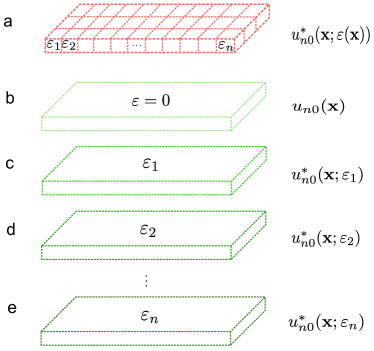
To proceed with our envelope function expansion for inhomogeneously strained crystals, we first imagine a series of strained crystals with different strain tensors , all of which are then mapped back to undeformed coordinates following the same coordinate transformation elaborated in the previous section. Fig. 1 illustrates this procedure. For a homogeneously strained crystal, we can choose the reference unstrained crystal such that the rotation component of the displacement field is zero, which allow the displacement to be be written as , namely . It then follows from Eq. 12 and Eq. 13 that the Schrödinger equation for homogeneously strained crystals transforms into undeformed coordinates as
| (16) |
Here, to distinguish the crystal potential of homogeneously strained crystal from that of inhomogeneously strained crystal, we have used the symbol to represent the mapped crystal potential of homogeneously strained crystal with strain tensor . From now on, and will be used to represent the crystal potentials of homogeneously strained crystals and inhomogeneously strained crystals respectively.
Given a reference crystal momentum for unstrained crystal, for each of the homogeneously strained crystal with strain tensor , their Bloch functions at the corresponding strained crystal momentum can be written as
| (17) |
can then be mapped back to undeformed coordinates and denoted by
| (18) |
Without loss of generality, hereafter we chose the reference crystal momentum , in which case only the periodic part of the Bloch functions will be retained.
For any value of strain , the mapped Bloch functions are periodic functions of the original, undeformed lattice translation vectors. Therefore, each of them can be expanded in undeformed coordinates in terms of a complete and orthonormal basis set , which for example can be plane waves:
| (19) |
The expansion coefficients will be dependent of the strain value . After this expansion, the strain dependence of the Bloch functions is separated into the expansion coefficients . In the absence of strain-induced phase transition, and choosing the same gauge Marzari et al. (2012) for different strained Bloch functions, these expansion coefficients should be continuous functions of strain . We then can define a strain-parametrized basis set , which means that at position , the values of the expansion coefficients in Eq. 19 take the values of . Mathematically, this can be written out as
| (20) |
are named “strain-parametrized Bloch functions”, since they are parametrized to the strain field in an inhomogeneous strained crystal. In analogy with the conventional envelope function method,Luttinger and Kohn (1955) we can use to expand the mapped global wavefunctions of inhomogeneously strained crystals,
| (21) |
The summation is over the band index , but will normally be truncated to include only bands within certain energy range of interest, as far-away bands have smaller contributions to the electronic states under consideration. Here, are, as in conventional envelope function method, considered to be smooth functions on unit-cell scale. This envelope expansion is, in essence, a continuous generalization of Bastard’s envelope expansion method for semiconductor heterostructures,Bastard (1981) where the wavefunctions in the barrier and well regions of heterostructures are expanded in the Bloch functions of respective region.
II.3 Local Approximation of Strained Crystal Potential and Envelope Function Equation
Our next natural step is to substitute into the mapped Schödinger equation for inhomogeneously strained crystal, the Eq. 12, which for convenience is rewritten here as
| (22) |
where is an operator given by
| (23) |
and have been defined earlier. Replacing by the strain-parametrized envelope function expansion in Eq. 21, the above Schrödinger equation becomes
| (24) |
The potential energy operator is the unknown term in the Hamiltonian, which in ab initio calculation is determined self-consistently. As we have argued earlier, such self-consistent calculation of is usually impractical for an inhomogeneously strained crystal due to the large system size. Hence, we introduce here an important approximation in our method: for a slowly-varying inhomogeneously strained semiconductor, the crystal potential at position can be well approximated by that of a homogeneously deformed crystal with same strain tensor , if (a) the applied elastic strain field is sufficiently slowly-varying at atomic scale and (b) long-range electrostatic effects Van de Walle and Martin (1989) are negligible. This locality principle for the electronic structure of insulators/semiconductors has been proved by E et al. E and Lu (2010, 2011, 2013) It is also implicitly implied in the treatment of strain in the EPM method. Wang and Zunger (1999) We also note that, the limitation of local approximation to the effective potential in the envelope function method has been studied by other authors Milanović and Tjapkin (1982); Foreman (2007); Yoo et al. (2010); Flores-Godoy et al. (2013).
Mathematically, the locality principle translates into , where is the strain-parametrized crystal potential of homogeneously strained crystals, is the average magnitude of lattice constants, and is the gradient of strain field. is thus a measure of how fast strain varies at atomic scale. Clearly, the smaller this measure, the better the locality approximation will be. In the case goes to zero, the approximation becomes exact. Since we are concerned with slowly-varying inhomogeneously strained crystals in this article, in what follows we will only keep the term , which is the zeroth-order term in strain gradient, or the first-order term in displacement gradient.
Adopting this locality principle greatly facilitates the solution of the electronic structure problem, as we can now use the local electronic structure information of homogeneously deformed crystals, obtained from unit-cell level ab initio or semi-empirical calculations, to eliminate the unknown crystal potential term in Eq. 24. Specifically, we can write down the local Schrödinger equation for the strain-parametrized expansion basis
| (25) |
with being
| (26) |
In Eq. 25, is the strain-parametrized energy eigenvalues for band at the reference crystal momentum, defined as . The subscript in denotes that, when the partial derivatives operate on the strain-parametrized expansion , they act on the position dependence coming from , but not on the dependence coming from . To better understand Eq. 25, one can look at the limit when the strain field is uniform throughout the crystal. Eq. 25 then simply becomes a normal Schrödinger equation for homogeneously strained crystal mapped to undeformed coordinates.
We will now use the local Schrödinger equation to eliminate the potential energy operator in global Schrödinger equation. Rearranging Eq. 25, we have
| (27) |
We then replace in Eq. 24 by based on the locality principle, and replace by the right-hand side of Eq. 27. Finally, we reach the following coupled differential equation for the envelope functions :
| (28) |
This coupled differential eigenvalue equation is the central equation we need to solve in our envelope function method. The unknowns in the equations are the global energy eigenvalues and their associated envelope functions . The strain-parametrized Bloch functions and their energy eigenvalues , can be constructed using ab inito or semi-empirical calculation of homogeneously strained crystals at unit-cell level, using the procedures described in Sec. II.2. The coupled differential equation can be solved numerically by expanding the envelope functions in an appropriate basis, and then turned into a matrix eigenvalue equation. The expansion basis can be judiciously chosen to reflect the symmetries that the envelope functions could have. The most general expansion basis, however, are plane waves:
| (29) |
Plugging the above equation into Eq. 28, it will turn into the following equation
| (30) |
We then multiply the both sides of Eq. 30 by (dagger denotes complex conjugation), and then integrate both side over the whole crystal volume . This results in independent linear equations, where is the number of bands included in the envelope function expansion in Eq. 21, is the number of plane waves used to expand the envelope functions in Eq. 29. The system of linear equations are written below as:
| (31) |
where
is short for . The system of linear equations can be solved numerically as a generalized eigenvector problem to obtain the eigenvalues and eigenvectors .
III Application to One-Dimensional Models
III.1 General Framework
To demonstrate the effectiveness of our envelope function method, we will apply the method to one-dimensional (1D) inhomogeneously strained crystals. We will first lay out the general mathematical framework of the method in 1D, followed by a specific example in the next section. Most equations in this section are just 1D special cases of equations in the previous section.
Suppose a slowly varying inhomogeneous strain is imposed on a 1D crystal. The strain field corresponds to a displacement field . The operators and defined in the previous section will have the following form
| (32) | |||
| (33) |
where denotes the derivative of strain with respect to . The partial derivative in implies that, for a strain parametrized function , the derivative will not act on the dependence coming from .
The Schrödinger equation mapped back to undeformed coordinates will be
| (34) |
where and are mapped crystal potential and energy eigenfunction in undeformed coordinates. is energy eigenvalue. will be expanded in terms of envelope functions and strain-parametrized Bloch functions:
| (35) |
The strain parametrized Bloch functions satisfies the local Schrödinger equation for homogeneously strained crystal
| (36) |
We then adopt the local approximation of crystal potential , which allows us to use the above local Schrödinger equation to transform Eq. 34 into the following envelope function equation
| (37) |
Using the explicit forms of and in Eq. 32 and Eq. 33, the above equation can be further written as
| (38) |
with , , and given by
| (39) |
After constructing the strain parametrized Bloch functions and through unit-cell level calculations of homogeneously strained crystals and strain-parametrization, described in Sec. II.2, the coupled differential eigenvalue equation Eq. 38 can be solved numerically using the method described in the previous section.
III.2 Example
Consider a 1D crystal with lattice constant and the following model crystal potential
| (40) |
This crystal potential has the following attractive features:
(1) A direct bandgap of magnitude will open up between the second and third energy band at crystal momentum , as shown in Fig. 2. Assuming that the first and second band are completely filled by electrons while those bands above are empty, the 1D crystal corresponds to a direct bandgap semiconductor for which the second band () is the “valence band” and the third band () is the “conduction band”. We will use this designation from now on. The bandgap is , where is the energy of the conduction band minimum, and is the energy of the valence band maximum.
(2) If we fix , the value of bandgap will almost have no change even when the lattice constant is varied. The change of lattice constant is natural when we apply strain to the system, namely becomes . While does not change when lattice constant is changed, the absolute energy values of the conduction band edge and valence band edge , however, do shift, mainly due to the change of kinetic energies for electrons in the system when enlarging or shrinking the crystal. we can therefore model the strain-induced energy level shifting without incurring bandgap change in this model crystal potential.
(3) If we want to model bandgap change when strain is applied, we can simply write as a function of strain . For example, to model the linear change of bandgap as a function of strain, we can write , where denotes the rate of bandgap change as a function of strain.
Hence, the 1D crystal potential is an excellent model system for 1D semiconductor, whose band edge energy levels and bandgap can be independently tuned. The crystal potential can therefore model deformation potential Bardeen and Shockley (1950) while being mathematically simple and transparent.
In the spirit of the above discussion, we now assume that, after applying homogeneous strain to the model 1D semiconductor, its crystal potential has the following form:
| (41) |
This implies that both the energy levels and bandgap of the 1D crystal will change after applying strain. Comparison of the band-structures of the 1D crystal before and after deformation for a specific set of parameters , , and is shown in Fig. 2.

The crystal potential of homogeneously strained 1D crystal, , is up to now defined in strained coordinates . As discussed earlier, we can map the strained crystal potential back to undeformed coordinates based the mapping relationship . The mapped crystal potential becomes the following
| (42) |
Suppose now a continuous strain distribution is defined in the coordinates. We can define a strain-parametrized crystal potential such that at position , we first calculate the strain at , then assign a value equal to . Namely,
| (43) |

With the above model set-up, we now apply a Gaussian-type inhomogeneous strain on the 1D crystal. The strain distribution is given by
| (44) |
where is the maximum strain value in the strain field , occurring at . denotes the size of crystal. After applying the inhomogeneous strain, a position in the undeformed crystal will map to a new position in deformed coordinates given by
| (45) |
where denotes error function.
Denote by the crystal potential of the 1D crystal after applying the Gaussian inhomogeneous strain, we then adopt the local approximation of crystal potential as described in Sec. II.3, which says that the inhomogeneously strained crystal potential at point can be well approximated by the crystal potential of a homogeneously strained crystal with the same strain value. This can be mathematically written out as
| (46) |
The as-constructed strained crystal potential is visualized in Fig. 3.
We have thus, for demonstration purpose, explicitly constructed the strained crystal potential using the local approximation of crystal potential. This allows us to solve the energy eigenstates of an inhomogeneously strained crystal using two distinct methods:
Method 1: direct numerical diagonalization of strained Hamiltonian. Since the explicit expression for the inhomogeneously strained crystal potential has been constructed, we can solve the Schrödinger equation for the inhomogeneously strained crystal in deformed coordinates,
| (47) |
by diagonalizing the Hamiltonian using plane wave basis set in Fourier space. More straightforwardly, we can discretize the wavefunction into a matrix vector in real space,
| (48) |
and then write the Hamiltonian as a matrix operator acting on the wavefunction , where and are the matrix operators for the differential operator and the potential operator respectively:
| (49) |
| (50) |
is the distance between two real space grid points. The Hamiltonian matrix can then be numerically diagonalized to obtain the energy eigenvalues and wavefunctions .
Method 2: solving the energy eigenstates of inhomogeneously strained crystal using our envelope function method. We can solve the Schrödinger equation, Eq. 47, by first mapping it back to undeformed coordinates, which becomes
| (51) |
The explicit expression for the differential operator is given by Eq. 32. The mapped wavefunctions will then be expressed in terms of envelope functions and strain-parametrized Bloch functions :
| (52) |
We then follow the procedures described in Sec. III.1 to eliminate the crystal potential term in Eq. 51 using strain-parametrized Bloch functions and the associated strain-parametrized energy eigenvalues . Eq. 51 can then be turned into a coupled differential eigenvalue equation for the envelope functions given by Eq. 38, and solved as a generalized matrix eigenvector problem.
The solution of Eq. 38 requires the explicit construction of strain-parametrized functions and the associated strain-parametrized energy eigenvalues . The construction of these functions involves unit-cell level calculations of homogeneously strained 1D crystals. Only the Bloch functions and energy eigenvalues of the electronic states at the reference crystal momentum ( in this case) and a few bands close to the valence/conduction band need to be calculated. The homogeneous strain values are coarsely taken from the inhomogeneous strain field (no more than one grid point per unit cell). The calculated periodic Bloch functions of each homogeneously strained crystal are then expressed in plane wave basis as , where are the expansion coefficients. The strain-parametrized Bloch functions can then be constructed by letting at position , namely
| (53) |
It is easy to see that, at position , the value of is the same as the value of periodic Bloch function at and . It is in this sense are named strain-parametrized functions. Since are smooth functions of and is a smooth function of , we can use polynomial fitting to obtain smooth functions for . As only unit-cell level calculations of homogeneously strained crystals at a reference crystal momentum are involved, the construction of the strain-parametrized functions and do not require much computational power in this 1D example.
Of the two methods discussed above, Method 1, the direct diagonalization of Hamiltonian, is a well established method, therefore it can be used to benchmark Method 2, our envelope function method. To test the effectiveness of our envelope function method, we have calculated the energy eigenvalues and eigenfunctions of the 1D inhomogeneously strained crystal using both methods. A special note is that we are not testing here how good the local approximation of crystal potential for inhomogeneously strained crystal can be, but how accurate and fast our envelope function method can achieve given the local approximation of crystal potential is a sufficiently good approximation. Also note that, although for the sake of benchmarking our envelope function method, we have explicitly constructed the strained crystal potential in this 1D problem, in practical application of our envelope function method, such explicit construction of crystal potential will not be performed. The information of local strained crystal potential, at the level of approximation used in our method, is reflected in the strain-parametrized Bloch functions and the associated strain-parametrized energy eigenvalues .
Choosing the following model parameters , , , and for the 1D inhomogeneously strained crystal, we carry out numerical real space diagonalization of the Hamiltonian by spatially discretizing the wavefunction into a matrix. Periodic boundary condition is adopted. As the wavefunction oscillates rapidly even within a unit cell, very large , around 50 times the number of unit cell , is needed to achieve convergence of energy eigenvalues near valence or conduction band edge.
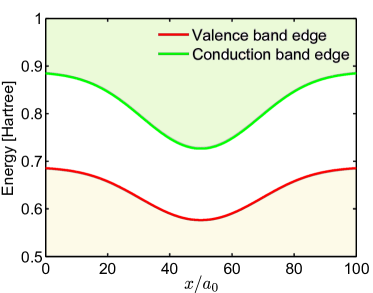
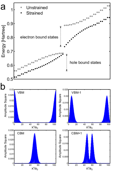
Fig. 4a shows the direct-diagonalization obtained energy eigenvalues near the band edges. A Hamiltonian matrix is involved in the numerical calculation. For comparison, the energy eigenvalues of unstrained crystal are shown together in the figure. The most distinct feature for the energy spectrum of inhomogeneously strained crystal is the appearance of bound states near the conduction and valence band edges. These bound states, whose wavefunctions are shown in Fig. 4b, can be understood by plotting the local valence and conduction band edges as a function of position in the strained crystal, which is shown in Fig. 5. The alignment of band edges is reminiscent of semiconductor quantum well, except that in our case, the spatial variation of band-edge is smooth and extended, while in semiconductor quantum well, band edge usually jumps abruptly at the interface between the barrier and well region of quantum well. Hence, the strain-confined bound states in inhomogeneously strained crystal bear resemblance to bound states in quantum well. We want to emphasize that, the band edge alignment in our 1D inhomogeneously strained crystal is not unique to this model. Strain-induced band edge shift in semiconductor is a well-known phenomenon.Bardeen and Shockley (1950) In fact, the band-edge alignment in our 1D model is similar to those calculated by Feng et al for inhomogeneously strained MoS2 monolayer. Feng et al. (2012) We can therefore conclude that the existence of electron or hole bound states is a general feature in an inhomogeneously strained crystal.
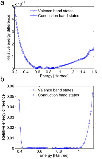
We have also calculated the energy eigenvalues using our envelope function method. As shown in Fig. 6a, very high accuracy of eigenvalues is achieved for the whole valence and conduction bands using only one mesh grid per unit cell representation of the envelope functions. The lowest five bands are included in the summation over bands in the envelope function expansion (Eq. 52). Together, the envelope function method involves the diagonalization of an approximately by matrix, which is an order of magnitude smaller than direct diagonalization. As zone-center Bloch functions are used to carry out envelope function expansion, naturally the error for energy eigenvalues near the band edge is smaller, same as in conventional envelope function method. Furthermore, if one is only concerned with energy levels near the band edge, which in most practical application is true, the expense of envelope function method can be reduced by another order of magnitude by including only the most relevant bands, and using coarser grids for numerical representation of the envelope functions. In Fig. 6b, we show that more than 1/4 of energy levels in valence and conduction bands can be calculated with very high accuracy by including only the valence and conduction bands in wavefunction expansion, and using one mesh grid every four unit cells to represent the envelope functions. In this case, one ends up diagonalizing a by matrix, which is two order of magnitude smaller than direct diagonalization. Indeed, for this 1D model, our envelop function method is much faster than the direct diagonalization method.
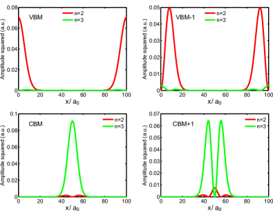
The success of the envelope function method is because the envelope functions are indeed slowly varying as we conjectured. Fig. 7 shows the amplitude square plot of envelope functions for a few electron and hole bound states. For the electron bound states, the envelope function of conduction band is predominant, while the valence band envelope function also contributes. The opposite is true for the hole bound states. Other remote bands have negligible contribution and are therefore not plotted. Comparing with the full wavefunctions calculated from direct diagonalization in Fig. 4b, one can notice that the envelope functions are indeed slowly-varying functions modulating the amplitude of fast-varying Bloch functions.
IV Toward Application to Three-Dimensional Real Materials
We have demonstrated in the previous section that our envelope function method can be successfully applied to a model 1D slowly-varying inhomogeneously strained semiconductor. A real semiconductor, however, is a three-dimensional (3D) object, and its crystal potential and strain response will be more complicated than the 1D model. Therefore, in this section we discuss some of the issues that may arise when applying our method to real 3D semiconductor crystals.
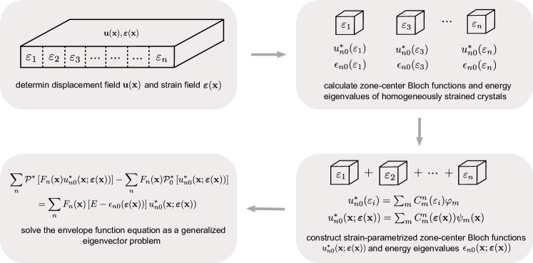
The procedures to carry out our envelope function method in 3D are essentially the same as in 1D, which we summarize in the flow chart of Fig. 8.
The first step in the flow chart is the determination of a smooth displacement field which can map the unstrained crystal (and the associated vacuum space, if any) to the strained crystal. The corresponding strain field needs to be calculated as well. In 1D, displacement field is a one-dimensional function and contains no rotational component. Thus is related to the strain field via a simple integral relation . In 3D, the displacement field is three-dimensional, and the strain field is a tensor field with six independent components. Due to the possible existence of rotational components, the components of the strain field are related to the displacement field (in the small deformation limit) as:
| (54) |
Hence, for a generic 3D inhomogeneously strained crystal, finding and representing the smooth displacement field and strain field becomes more difficult than 1D. Knowledge of solid mechanics will be helpful in this endeavor. The increased complexity of the displacement field and strain field in 3D also complicates the calculation and representation of the differential operators and defined in Eq. 23 and Eq. 26, which need to be determined in order to solve the envelope function equation, Eq. 28.
The second and third step in the flow chart are the construction of strain-parametrized Bloch functions and associated strain-parametrized energy eigenvalues at a reference crystal momentum, usually at the Brillouin zone center, through ab initio or semi-empirical electronic structure calculation of a series of homogeneously strained crystal. The strain values are coarsely taken from the inhomogeneous strain field , which in principle is sufficient as the strain field is slowly-varying in space. Nevertheless, in a generic 3D case this step will be challenging as the number of calculations for homogeneously strained crystal can become quite large if the strain field is complex, as there are six independent components of strain tensor in 3D. The construction of strain-parameterized Bloch functions, described in Sec. II.2, might also become non-trivial due to the complexity of electronic wavefunctions in 3D. Proper choice of expansion basis for the Bloch functions in Eq. 19 and Eq. 20 will be essential.
The fourth step in the flow chart is the solution of coupled differential equation for the envelope functions, the Eq. 28. This step, having been discussed in Sec. II.3, should be straightforward once the differential operators and , strain parameterized Bloch functions and the associated strain parameterized energy eigenvalues have all been determined in the previous steps. Nevertheless, the computational cost of solving the differential eigenvalue equation will become larger as the dimensionality of the problem increases, as more spatial or Fourier grids will be needed to represent the envelope functions , resulting in larger matrices for numerical diagonalization.
In summary, the application of our envelope function method to a generic 3D problem will be feasible but challenging. We therefore believe that our method will most likely find applications in cases where the 3D problem is quasi-1D or 2D, namely when only one or very few components of the strain tensor is varying slowly in space.
We also comment here a few issues related to the central approximation adopted in our method, the local approximation of crystal potential in strained crystal elaborated in Sec. II.3. The approximation states that in a slowly-varying inhomogeneously strained semiconductor or insulator, the local crystal potential can be well approximated by that of a homogeneously strained crystal with the same strain tensor . This local approximation of strained crystal potential is likely to be a good approximation only for non-polar semiconductors such as silicon and germanium. For polar semiconductors such as gallium arsenide, strain could induce piezoelectric effect, which generates long-range electric field in the deformed crystal and significantly increases the error of this approximation. Furthermore, we note that for certain materials with more than one atoms within a unit cell, strain can induce internal relaxation of atoms relative to each other on top of the displacement described by strain tensor, an effect not included in our present method and must be carefully checked in realistic calculations.
V Envelope Function Equation for Empirical Applications
In this section, we will cast the envelope function equation (Eq. 28) in a new form in which the strain-parametrized Bloch functions will not appear explicitly. They will be replaced by a set of matrix elements involving their integrals. Doing so allows the method to be used empirically, where the matrix elements can be fitted to experimental data. The connection to traditional envelope function method will also become clearer. For convenience, we rewrite the relevant equations below
| (55) |
where
| (56) | |||
| (57) |
and are given by
| (58) | |||
| (59) |
can be expanded out as
| (60) |
In above expansion, we have used the symmetry property of , namely .
When strain variation is varying slowly at atomic scale, which is the premise of our envelope function method, the strain-parametrized basis functions for different bands are approximately independent and orthogonal:
| (61) |
The integration is over the whole crystal, whose volume is . The Jacobian of deformation map takes into account the change of volume elements during coordinate transformation. We also note that, can be absorbed into the basis functions by re-defining as , and the whole formalism of our envelope function method will not change. This can be sometimes be more convenient for constructing strain-parametrized basis set.
Using the above orthonormal relation, we can express , , and in terms of as
where , and are matrix elements given by
Eq. 55 can now be written in terms of as
| (62) |
Equating coefficients of on both side,Burt (1992) we arrives at a new form of envelope function equation
| (63) |
In the equation, and are related to deformation mapping and can be calculated once the displacement field is known. and can be calculated either by constructing the strain-parametrized basis set or fit empirically to experimental data. As a sanity check, when a crystal is undeformed, namely , we have , , , , , and the envelope function equation will become
| (64) |
with being
| (65) |
Eq. 64 recovers the envelope function equation for bulk crystals.Burt (1992)
VI Summary and Conclusion
To summarize, we have developed a new envelope function formalism for electrons in slowly-varying inhomogeneously strained crystals. The method expands the electronic wavefunctions in a smoothly deformed crystal as the product of slowly varying envelope functions and strain-parametrized Bloch functions. Assuming, with justifications, that the local crystal potential in a smoothly deformed crystal can be well approximated by the potential of a homogeneously deformed crystal with the same strain value, the unknown crystal potential in Schrödinger equation can be replaced by the a small set of strain-parametrized Bloch functions and the associated strain-parametrized energy eigenvalues at a chosen crystal momentum. Both the strain-parametrized Bloch functions and strain-parametrized energy eigenvalues can be constructed from ab initio or semi-empirical electronic structure calculation of homogeneously strained crystals at unit-cell level. The Schrödinger equation can then be turned into eigenvalue differential equations for the envelope functions. Due to the slowly-varying nature of the envelope functions, coarse spatial or fourier grids can be used to represent the envelope functions, therefore enabling the method to deal with relatively large systems. Compared to the traditional multi-band envelope function method, our envelope function method has the advantage of keeping unit-cell level microstructure information since the local electronic structure information is obtained from ab initio or EPM calculations. Compared to the conventional EPM method, our method uses envelope function formalism to solve the global electronic structure, therefore has the potential to reduce the computational cost. The method can also be used empirically by fitting the parameters in our derived envelope function equations to experimental data. Our method thus provides a new route to calculate the electronic structure of slowly-varying inhomogeneously strained crystals.
VII Acknowledgements
We acknowledge financial support by NSF DMR-1120901. Computational time on the Extreme Science and Engineering Discovery Environment (XSEDE) under the grant number TG-DMR130038 is gratefully acknowledged.
References
- Li et al. (2014) J. Li, Z. Shan, and E. Ma, MRS Bull. 39, 108 (2014).
- Novoselov et al. (2005) K. S. Novoselov, D. Jiang, F. Schedin, T. J. Booth, V. V. Khotkevich, S. V. Morozov, and A. K. Geim, Proc. Natl. Acad. Sci. U. S. A. 102, 10451 (2005).
- Lee et al. (2008) C. Lee, X. D. Wei, J. W. Kysar, and J. Hone, Science 321, 385 (2008).
- Liu et al. (2007) F. Liu, P. M. Ming, and J. Li, Phys. Rev. B 76, 064120 (2007).
- Bertolazzi et al. (2011) S. Bertolazzi, J. Brivio, and A. Kis, ACS Nano 5, 9703 (2011).
- Feng et al. (2012) J. Feng, X. F. Qian, C. W. Huang, and J. Li, Nat. Photonics 6, 866 (2012).
- Slater and Koster (1954) J. C. Slater and G. F. Koster, Phys. Rev. 94, 1498 (1954).
- Di Carlo (2003) A. Di Carlo, Semicond. Sci. Technol. 18, R1 (2003).
- Zunger (1998) A. Zunger, MRS Bull. 23, 35 (1998).
- Canning et al. (2000) A. Canning, L. W. Wang, A. Williamson, and A. Zunger, J. Comput. Phys. 160, 29 (2000).
- Wang and Zunger (1999) L. W. Wang and A. Zunger, Phys. Rev. B 59, 15806 (1999).
- Luttinger and Kohn (1955) J. M. Luttinger and W. Kohn, Phys. Rev. 97, 869 (1955).
- Bastard (1981) G. Bastard, Phys. Rev. B 24, 5693 (1981).
- Baraff and Gershoni (1991) G. A. Baraff and D. Gershoni, Phys. Rev. B 43, 4011 (1991).
- Gershoni et al. (1993) D. Gershoni, C. H. Henry, and G. A. Baraff, IEEE J. Quantum Electron. 29, 2433 (1993).
- Burt (1992) M. G. Burt, J. Phys.: Condens. Matter 4, 6651 (1992).
- Burt (1999) M. G. Burt, J. Phys.: Condens. Matter 11, R53 (1999).
- Wang and Zunger (1996) L. W. Wang and A. Zunger, Phys. Rev. B 54, 11417 (1996).
- Kane (1957) E. O. Kane, J. Phys. Chem. Solids 1, 249 (1957).
- Stier and Bimberg (1997) O. Stier and D. Bimberg, Phys. Rev. B 55, 7726 (1997).
- Stier et al. (1999) O. Stier, M. Grundmann, and D. Bimberg, Phys. Rev. B 59, 5688 (1999).
- Efros and Rosen (2000) A. L. Efros and M. Rosen, Annu. Rev. Mat. Sci. 30, 475 (2000).
- Bardeen and Shockley (1950) J. Bardeen and W. Shockley, Phys. Rev. 80, 72 (1950).
- Herring and Vogt (1956) C. Herring and E. Vogt, Phys. Rev. 101, 944 (1956).
- Bir and Pikus (1974) G. L. Bir and G. E. Pikus, Symmetry and Strain-Induced Effects in Semiconductors (Wiley, New York, 1974) p. 295.
- Zhang (1994) Y. Zhang, Phys. Rev. B 49, 14352 (1994).
- Chelikowsky and Cohen (1976) J. R. Chelikowsky and M. L. Cohen, Phys. Rev. B 14, 556 (1976).
- Wang and Zunger (1995) L. W. Wang and A. Zunger, Phys. Rev. B 51, 17398 (1995).
- Wood and Zunger (1996) D. M. Wood and A. Zunger, Phys. Rev. B 53, 7949 (1996).
- Fu et al. (1998) H. Fu, L. W. Wang, and A. Zunger, Phys. Rev. B 57, 9971 (1998).
- Whitfield (1961) G. D. Whitfield, Phys. Rev. 121, 720 (1961).
- E and Lu (2010) W. E and J. F. Lu, Commun. Pure Appl. Math. 63, 1432 (2010).
- E and Lu (2011) W. E and J. F. Lu, Arch. Ration. Mech. Anal. 199, 407 (2011).
- E and Lu (2013) W. E and J. F. Lu, Mem. Amer. Math. Soc. 221, No. 1040 (2013).
- Ericksen (2008) J. L. Ericksen, Math. Mech. Solids 13, 199 (2008).
- Marzari et al. (2012) N. Marzari, A. A. Mostofi, J. R. Yates, I. Souza, and D. Vanderbilt, Rev. Mod. Phys. 84, 1419 (2012).
- Van de Walle and Martin (1989) C. G. Van de Walle and R. M. Martin, Phys. Rev. Lett. 62, 2028 (1989).
- Milanović and Tjapkin (1982) V. Milanović and D. Tjapkin, Phys. Stat. Sol. (b) 110, 687 (1982).
- Foreman (2007) B. A. Foreman, Phys. Rev. B 76, 045327 (2007).
- Yoo et al. (2010) K. H. Yoo, J. D. Albrecht, and L. R. Ram-Mohan, American Journal of Physics 78, 589 (2010).
- Flores-Godoy et al. (2013) J. J. Flores-Godoy, A. Mendoza-Álvarez, L. Diago-Cisneros, and G. Fernández-Anaya, Phys. Status Solidi B 250, 1339 (2013).