Independent dynamic acousto-mechanical and electrostatic control of individual quantum dots in a LiNbO3-GaAs hybrid
Abstract
We demonstrate tuning of single quantum dot emission lines by the combined action of the dynamic acoustic field of a radio frequency surface acoustic wave and a static electric field. Both tuning parameters are set all-electrically in a LiNbO3-GaAs hybrid device. The surface acoustic wave is excited directly on the strong piezoelectric LiNbO3 onto which a GaAs-based p-i-n photodiode containing a single layer of quantum dots was epitaxially transferred. We demonstrate dynamic spectral tuning with bandwidths exceeding 3 meV of single quantum dot emission lines due to deformation potential coupling. The center energy of the dynamic spectral oscillation can be independently programmed simply by setting the bias voltage applied to the diode.
The random nature of the nucleation of epitaxial quantum dot (QD) nanosystems leads to an inhomogeneous broadening of the dots’ optical properties. Thus, reversible post-growth tuning mechanisms of the QD emission energy and occupancy states have been developed over the past 20 years. Here, the most established tuning parameter is a static electric field which can be simply set by tuning the bias voltage applied to a diode structure with embedded QDs. This tuning mechanism is routinely employed to control the occupancy state Drexler et al. (1994); Warburton et al. (2000) and emission energyFry et al. (2000) of QDs or coherent quantum couplings in QD-moleculesKrenner et al. (2005). More recently, staticSeidl et al. (2006); Ding et al. (2010) and dynamic strain Gell et al. (2008); Brüggemann et al. (2011) fields have proven to efficiently and independently tune the confined electronic and excitonic states of a QD. However, for novel quantum-optoelectronic devices and quantum logic protocols a combination of static and dynamic tuning parameters is of paramount importance. This sparked the idea to combine both tuning mechanisms to achieve full control over the QD’s optical propertiesTrotta et al. (2012a) which was crucial for realizing a highly reliable source of polarization entangled photon pairs Trotta et al. (2012b). Furthermore, to implement advanced quantum logic protocols based on Landau-Zener transitions in architectures based on optically active QDsBlattmann et al. (2014), tuning has to be performed at radio frequencies (rf). In this frequency band surface acoustic waves (SAWs) are an ideal candidate for dynamic tuning since these are accompanied by dynamic strain and piezoelectric components. Thus, they allow for acousto-mechanical and acousto-electric control of semiconductor nanostructures Rocke,
Zimmermann, Wixforth, Kotthaus, Böhm, and Weimann (1997); Rotter,
Kalameitsev, Govorov, Ruile, and Wixforth (1999); Kinzel,
Rudolph, Bichler, Abstreiter,
Finley, Koblmüller, Wixforth, and Krenner (2011), including in particular, the dynamic control of both the occupancy state Couto et al. (2009); Schülein et al. (2013); Weiß et al. (2014a) and emission energy Gell et al. (2008); Weiß et al. (2014b) of QDs. Because SAWs propagate almost dissipation-free over chip-scale distances, they natively address individual located along their propagation direction in parallel.
Here we demonstrate independent control of single QD emitters by dynamic strain and static electric field tuning in a hybrid device fabricated by epitaxial lift-off and transferRotter et al. (1997); Fuhrmann et al. (2010). Strain tuning is achieved by electrically exciting a SAW on a host substrate which interacts with QDs embedded in the active layer of a -based single QD-photodiode. We show that the latter allows for a global static electrical control of both the QD emission energy and occupancy state and the SAW provides a fast modulation around this statically defined center energy.
Our hybrid device is shown schematically in Fig.1(a). It consists of a LiNbO3 host substrate and an optically active GaAs based quantum dot structure as illustrated in Fig.1(b).
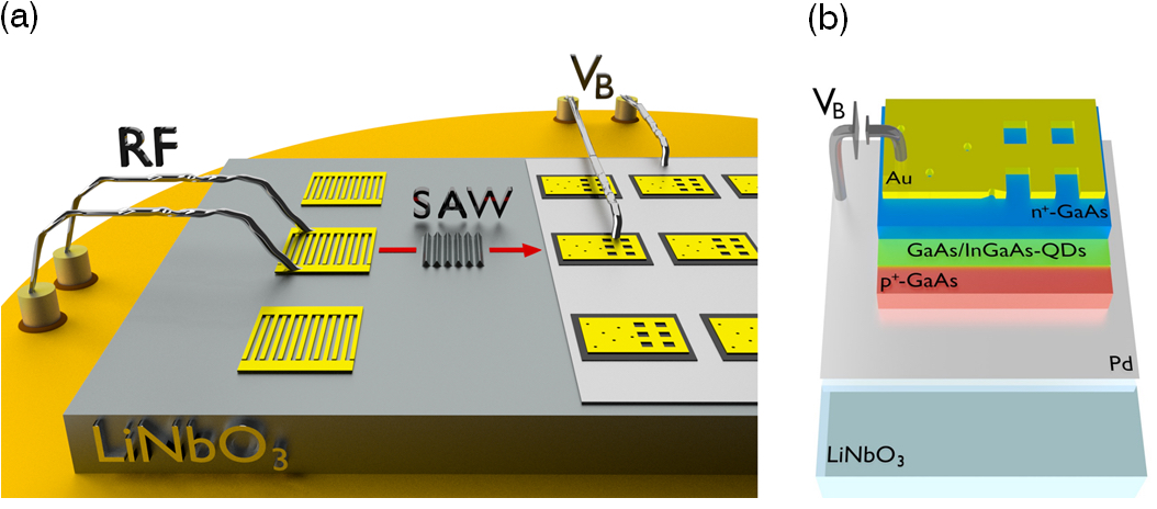
This structure was grown by molecular beam epitaxy (MBE) on a semi-insulating GaAs (100) substrate. After growth of a GaAs buffer layer, we deposited a 100 nm thick AlAs sacrificial layer for a selective wet chemical etching step. On top of this sacrificial layer, we grew 200 nm heavily p-doped GaAs followed by an undoped 35 nm GaAs buffer. Self-assembled QDs were formed by depositing 5 ML of In0.5Ga0.5As, which were subsequentially overgrown by 280 nm intrinsic GaAs and a 200 nm heavily n-doped GaAs contact. To generate SAWs on the chip, Ti/Au interdigital transducers (IDTs) with a resonant frequency (acoustic wavelength ) were fabricated prior transfer of the semiconductor film on a 128 ∘ rot YX LiNbO3 substrate. A 50 nm palladium (Pd) metallization was deposited at the later position of the semiconductor film. After fabrication of a 200 nm Au n-side contact equipped with shadow mask with 1 m diameter apertures to isolate single QDs. We epitaxially lifted off the diode structure from the GaAs substrate by selective HF-etching of the sacrificial layerYablonovitch et al. (1987, 1990). This 715 nm thick film was transferred onto the SAW-chip with the p-doped side on forming both a strong mechanical bond and good electrical contactYablonovitch et al. (1991) to the Pd layer. After transfer, we electrically isolated individual photodiodes by etching mesas.
Our experiments were performed in a liquid helium flow cold-finger cryostat at low temperature () using a conventional micro-photoluminescence (-PL) setup. For quasi-resonant photogeneration of charge carriers we used an externally triggered pulsed diode laser emitting pulses of a wavelength . The laser was focused by a 50 microscope objective to one of the aforementioned microapertures and the emitted PL of the QD was collected by the same objective and dispersed by a 0.5 m grating monochromator. Time-integrated detection was performed using a liquid N2 cooled Si-charge coupled device (CCD). The SAW was excited in pulsed mode (, on/off duty cycle 1:9,) to reduce spurious heating of the sample. To record the time-averaged SAW-modulation of the QD emission, we set , with being the laser repetition rate. In contrast, for time domain studies, we employed stroboscopic excitation and recorded time-integrated spectra for a fixed temporal delay (relative phase ) between laser and SAW over two full cycles from () Völk et al. (2011).
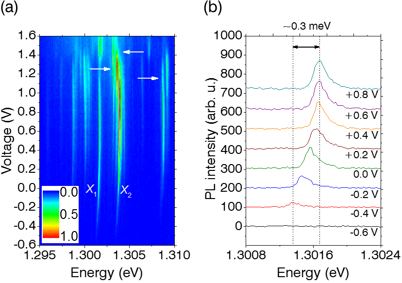
As a first step, we investigate the static bias voltage tuneability of single QDs in the epitaxially transferred p-i-n-diode. Typical PL spectra of a single QD are plotted in false color representation as a function of the applied bias voltage in Fig. 2 (a). At large negative no PL is detected due to tunnel extraction of carriers from the QD Müller et al. (2013). As is increased two prominent emission lines labeled ()and () can be distinguished. in the range . Both emission lines are observed over a relatively large range of and clear signatures of charging events (marked by arrows in Fig. 2 (b)) are detected for . Such behavior is readily expected for our diode structure due to the large injection barriers for electrons and holes which inhibit resonant tunnel injectionBaier et al. (2001). In addition to the occupancy state control, all emission lines exhibit clear spectral shifts arising from the quantum confined Stark effect (QCSE)Fry et al. (2000). Fig. 2 (b) shows selected spectra zooming in to the emission line for . From these data we extract a total shift , typical for these types of QDs in this diode structure. 111We want to note that both key characteristics, voltage control of the QD’s occupancy state and emission energy, have been observed with fully comparable performance on as-fabricated, but not epitaxially transferred devices.
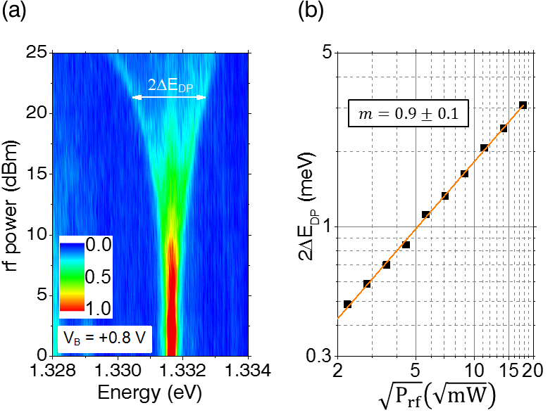
In a second step, we assess the dynamic acoustic tuning of the QD emission by a SAW. When applying a radio-frequency (rf) signal to the IDT, a SAW is generated on the LiNbO3, which is accompanied by a superposition of an electric and a strain field. As the SAW propagates across the epitaxially transferred photodiode, its electric field component is effectively screened by free carriers in the highly doped layers and the Pd metallization. As a direct consequence the QD response to the SAW is dominated by deformation potential (DP) coupling induced by the dynamic strain field. In Fig. 3 (a) we present time-integrated, non-stroboscopic emission spectra of a single QD emission line. 222This particular QD is located underneath a different microaperture on the same photodiode and exhibits a particularly pronounced strain tuning amplitude. The data are plotted in false color representation as a function of the applied rf power and a fixed bias voltage of . The emission intensity was averaged over the temporal delay, , to assess the full tuning bandwidthFuhrmann et al. (2011). Clearly, our data demonstrates a pronounced broadening of the emission lines as we increase to 333Due to the pulsed excitation scheme we observe a deviation from the line shape expected for a sinusoidally modulated Lorentzian line since since spectra were averaged over 80 laser pulses, i.e. 80 samples of . The total tuning bandwidth was determined from the total broadening (low energy to high energy edge) of the emission line Fuhrmann et al. (2011).. This broadening and thus spectral modulation induced by DP coupling continuously increases with increasing . For this particular QD it reaches a maximum of for the largest SAW amplitudes at . Over this large range of no signatures of a pronounced switching behavior between different emission lines i.e. occupancy states are detected. Such behavior studied in references Völk et al. (2010); Schülein et al. (2013); Weiß et al. (2014a) would be indicative of acousto-electrically driven charge carrier dynamics. Its absence provides evidence for a screening of the SAW-induced electric fields. The nature of the underlying physical mechanism can be identified by studying the modulation bandwidth as a function of the acoustic amplitude . While for DP coupling a linear dependence of on is expected, a dynamically driven QCSE should result in a quadratic dependence Santos et al. (2004); Weiß et al. (2014b). To identify such a power law dependence in our data, we plot the extracted from the total width of the emission peak (symbols) over in double-logarithmic representation in Fig. 3 (b). This analysis shows a clear linear behavior over the entire range of with no indications of additional contributions. From a best fit (line) we extract an exponent of , close to the ideal value of expected for DP coupling. Owing the fact that only a single tuning mechanism is at play, we can quantify the local hydrostatic pressure, , dynamically induced by the SAW from at . Using the established DP coupling strength in GaAs for [110] and [100] stresses given by the partial derivative of the band gap energy over the hydrostatic pressure, Pollak and Cardona (1968) we obtain a maximum hydrostatic pressure to .
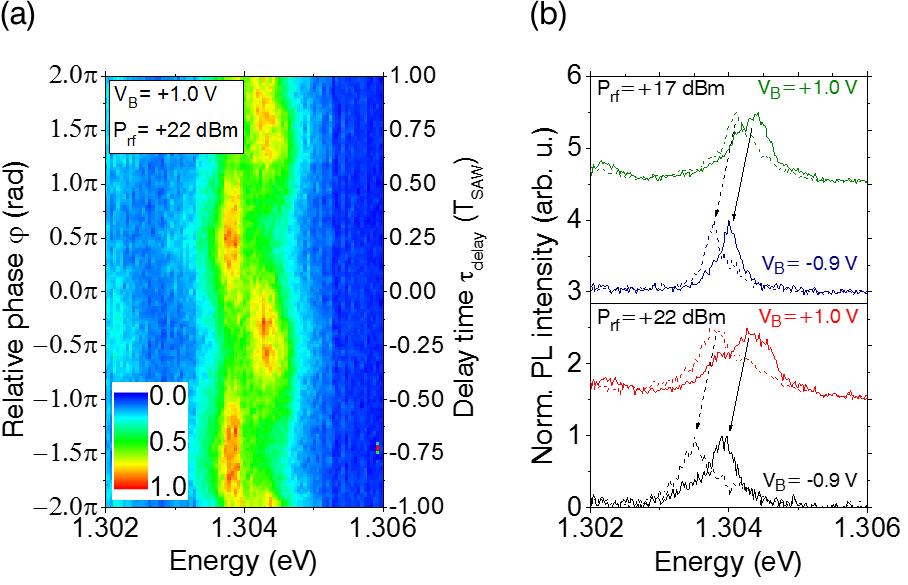
Finally we address the dynamic nature of the SAW-mediated emission control and its combination with the static electric field tuning. To confirm the time-domain spectral tuning we employed stroboscopic optical excitation. The obtained emission spectra of the emission line for fixed and are presented in Fig. 4 (a). The intensity is color coded and plotted as a function of photon energy and () over two full cycles from (). In these data, we resolve a clear spectral oscillation with the fundamental period of the SAW, which exhibits an amplitude of . These observations are in full agreement with a strain-driven modulation of the QD emission energy and no signatures arising from dynamic piezoelectric effects are resolvableWeiß et al. (2014b). In particular, the maxima at is at lower energies compared to the undisturbed case. This can be attributed to an introduced tensile strain. For the energetic shift is towards higher energy, indicative to maximum compressive strain. In the depicted example the peak to peak modulation amplitude is determined to be .
To demonstrate combined static and dynamic tuning employing the QCSE and SAW-driven DP tuning, we compare in Fig. 4(b) stroboscopic PL spectra recorded of at and for (upper panel) and (lower panel). The two stroboscopic spectra were taken at the minimum and maximum tuning of the DP tuning at (dashed lines) and (solid lines), respectively. Clearly, for both values of , tuning of leads to the desired static variation of the center energy of the SAW-driven DP modulation. In addition, the amplitude of the latter is preserved and constant within the resolution of our experiment since for the two chosen values of the recorded peak positions exhibit identical shifts due to the QCSE as indicated by the dashed and solid arrows. These findings nicely demonstrate independent control of single QD emission lines by static QCSE and dynamic DP tunings. Both parameters are programmed all electrically simply by applying a gate voltage to the photodiode or a rf signal to an IDT to launch a SAW.
In conclusion, we realized a LiNbO3-GaAs-hybrid device which enables to deliberately control the optical emission of a single QD by two independently accessible tuning parameters. The unique combination of dynamic acousto-mechanical control mediated by a rf SAW and an electro-statically, voltage-controlled Stark shift opens directions to add a fast modulation at an arbitrary set transition energy. In our present experiments both “tuning knobs” exhibit similar spectral tuning bandwidth. While that of the SAW modulation is mainly dependent on the type of substrate, that of the QCSE-tuning could be dramatically enhanced by introducing AlGaAs barriersBennett et al. (2010); Trotta et al. (2012b) or by replacing the QDs by columnar quantum posts with large QCSE Krenner et al. (2008). The demonstrated unique combination of dynamic and static tunings can be employed to implement dynamic quantum gate operations Blattmann et al. (2014) in QD-molecules for which the inter-dot couplings are sensitive to both, electric fieldsKrenner et al. (2005) and strain Zallo et al. (2014). Finally we note, that even largeMichaelis de Vasconcellos et al. (2010) electrical contacts allow for rf modulation also of the QCSE. A combination of rf electrical and acoustic offers an alternative route to realize dynamic quantum gates employing shaped control pulsesBlattmann et al. (2014).
We gratefully acknowledge financial support by Deutsche Forschungsgemeinschaft (DFG) within the framework of SFB 631 and the Emmy Noether Program (KR3790/2-1). KM acknowledges financial support from the Alexander von Humboldt Foundation.
References
- Drexler et al. (1994) H. Drexler, D. Leonard, W. Hansen, J. P. Kotthaus, and P. M. Petroff, “Spectroscopy of quantum levels in charge-tunable quantum dots,” Physical Review Letters 73, 2252–2255 (1994).
- Warburton et al. (2000) R. J. Warburton, C. Schäflein, D. Haft, F. Bickel, A. Lorke, K. Karrai, J. M. Garcia, W. Schoenfeld, and P. M. Petroff, “Optical emission from a charge-tunable quantum ring,” Nature (London) 405, 926–929 (2000).
- Fry et al. (2000) P. W. Fry, I. E. Itskevich, D. J. Mowbray, M. S. Skolnick, J. J. Finley, J. A. Barker, E. P. O’Reilly, L. R. Wilson, I. A. Larkin, P. A. Maksym, M. Hopkinson, M. Al-Khafaji, J. P. R. David, A. G. Cullis, G. Hill, and J. C. Clark, “Inverted Electron-Hole Alignment in Self-Assembled Quantum Dots,” Physical Review Letters 84, 733–736 (2000).
- Krenner et al. (2005) H. J. Krenner, M. Sabathil, E. C. Clark, A. Kress, D. Schuh, M. Bichler, G. Abstreiter, and J. J. Finley, “Direct Observation of Controlled Coupling in an Individual Quantum Dot Molecule,” Physical Review Letters 94, 57402 (2005).
- Seidl et al. (2006) S. Seidl, M. Kroner, A. Högele, K. Karrai, R. J. Warburton, A. Badolato, and P. M. Petroff, “Effect of uniaxial stress on excitons in a self-assembled quantum dot,” Applied Physics Letters 88, 203113 (2006).
- Ding et al. (2010) F. Ding, R. Singh, J. D. Plumhof, T. Zander, V. Křápek, Y. H. Chen, M. Benyoucef, V. Zwiller, K. Dörr, G. Bester, A. Rastelli, and O. G. Schmidt, “Tuning the Exciton Binding Energies in Single Self-Assembled InGaAs/GaAs Quantum Dots by Piezoelectric-Induced Biaxial Stress,” Physical Review Letters 104, 67405 (2010).
- Gell et al. (2008) J. R. Gell, M. B. Ward, R. J. Young, R. M. Stevenson, P. Atkinson, D. Anderson, G. A. C. Jones, D. A. Ritchie, and A. J. Shields, “Modulation of single quantum dot energy levels by a surface-acoustic-wave,” Applied Physics Letters 93, 81115 (2008).
- Brüggemann et al. (2011) C. Brüggemann, A. V. Akimov, A. V. Scherbakov, M. Bombeck, C. Schneider, S. Höfling, A. Forchel, D. R. Yakovlev, and M. Bayer, “Laser mode feeding by shaking quantum dots in a planar microcavity,” Nature Photonics 6, 30–34 (2011).
- Trotta et al. (2012a) R. Trotta, P. Atkinson, J. D. Plumhof, E. Zallo, R. O. Rezaev, S. Kumar, S. Baunack, J. R. Schröter, A. Rastelli, and O. G. Schmidt, “Nanomembrane quantum-light-emitting diodes integrated onto piezoelectric actuators.” Advanced Materials 24, 2668–72 (2012a).
- Trotta et al. (2012b) R. Trotta, E. Zallo, C. Ortix, P. Atkinson, J. D. Plumhof, J. van den Brink, A. Rastelli, and O. G. Schmidt, “Universal Recovery of the Energy-Level Degeneracy of Bright Excitons in InGaAs Quantum Dots without a Structure Symmetry,” Physical Review Letters 109, 147401 (2012b).
- Blattmann et al. (2014) R. Blattmann, H. J. Krenner, S. Kohler, and P. Hänggi, “Entanglement creation in a quantum-dot–nanocavity system by Fourier-synthesized acoustic pulses,” Physical Review A 89, 012327 (2014).
- Rocke et al. (1997) C. Rocke, S. Zimmermann, A. Wixforth, J. P. Kotthaus, G. Böhm, and G. Weimann, “Acoustically Driven Storage of Light in a Quantum Well,” Physical Review Letters 78, 4099–4102 (1997).
- Rotter et al. (1999) M. Rotter, A. V. Kalameitsev, A. O. Govorov, W. Ruile, and A. Wixforth, “Charge Conveyance and Nonlinear Acoustoelectric Phenomena for Intense Surface Acoustic Waves on a Semiconductor Quantum Well,” Physical Review Letters 82, 2171–2174 (1999).
- Kinzel et al. (2011) J. B. Kinzel, D. Rudolph, M. Bichler, G. Abstreiter, J. J. Finley, G. Koblmüller, A. Wixforth, and H. J. Krenner, “Directional and dynamic modulation of the optical emission of an individual GaAs nanowire using surface acoustic waves.” Nano Letters 11, 1512–1517 (2011).
- Couto et al. (2009) O. D. D. Couto, S. Lazić, F. Iikawa, J. A. H. Stotz, U. Jahn, R. Hey, and P. V. Santos, “Photon anti-bunching in acoustically pumped quantum dots,” Nature Photonics 3, 645–648 (2009).
- Schülein et al. (2013) F. J. R. Schülein, K. Müller, M. Bichler, G. Koblmüller, J. J. Finley, A. Wixforth, and H. J. Krenner, “Acoustically regulated carrier injection into a single optically active quantum dot,” Physical Review B 88, 085307 (2013), arXiv:1306.5954 .
- Weiß et al. (2014a) M. Weiß, F. J. R. Schülein, J. B. Kinzel, M. Heigl, D. Rudolph, M. Bichler, G. Abstreiter, J. J. Finley, A. Wixforth, G. Koblmüller, and H. J. Krenner, “Radio frequency occupancy state control of a single nanowire quantum dot,” Journal of Physics D: Applied Physics 47, 394011 (2014a).
- Weiß et al. (2014b) M. Weiß, J. B. Kinzel, F. J. R. Schülein, M. Heigl, D. Rudolph, S. Morkötter, M. Döblinger, M. Bichler, G. Abstreiter, J. J. Finley, G. Koblmüller, A. Wixforth, and H. J. Krenner, “Dynamic Acoustic Control of Individual Optically Active Quantum Dot-like Emission Centers in Heterostructure Nanowires.” Nano letters 14, 2256–64 (2014b).
- Rotter et al. (1997) M. Rotter, C. Rocke, S. Böhm, A. Lorke, A. Wixforth, W. Ruile, and L. Korte, “Single-chip fused hybrids for acousto-electric and acousto-optic applications,” Applied Physics Letters 70, 2097–2099 (1997).
- Fuhrmann et al. (2010) D. A. Fuhrmann, H. J. Krenner, A. Wixforth, A. Curran, K. A. Prior, R. J. Warburton, and J. Ebbecke, “Noninvasive probing of persistent conductivity in high quality quantum wells using surface acoustic waves,” Journal of Applied Physics 107, 93717 (2010).
- Yablonovitch et al. (1987) E. Yablonovitch, T. Gmitter, J. P. Harbison, and R. Bhat, “Extreme selectivity in the lift-off of epitaxial GaAs films,” Applied Physics Letters 51, 2222 (1987).
- Yablonovitch et al. (1990) E. Yablonovitch, D. M. Hwang, T. J. Gmitter, L. T. Florez, and J. P. Harbison, “Van der Waals bonding of GaAs epitaxial liftoff films onto arbitrary substrates,” Applied Physics Letters 56, 2419 (1990).
- Yablonovitch et al. (1991) E. Yablonovitch, T. Sands, D. M. Hwang, I. Schnitzer, T. J. Gmitter, S. K. Shastry, D. S. Hill, and J. C. C. Fan, “Van der Waals bonding of GaAs on Pd leads to a permanent, solid-phase-topotaxial, metallurgical bond,” Applied Physics Letters 59, 3159 (1991).
- Völk et al. (2011) S. Völk, F. Knall, F. J. R. Schülein, T. A. Truong, H. Kim, P. M. Petroff, A. Wixforth, and H. J. Krenner, “Direct observation of dynamic surface acoustic wave controlled carrier injection into single quantum posts using phase-resolved optical spectroscopy,” Applied Physics Letters 98, 23109 (2011).
- Müller et al. (2013) K. Müller, A. Bechtold, C. Ruppert, T. Kaldewey, M. Zecherle, J. S. Wildmann, M. Bichler, H. J. Krenner, J. M. Villas-Bôas, G. Abstreiter, M. Betz, and J. J. Finley, “Probing ultrafast carrier tunneling dynamics in individual quantum dots and molecules,” Annalen der Physik 525, 49–58 (2013).
- Baier et al. (2001) M. Baier, F. Findeis, A. Zrenner, M. Bichler, and G. Abstreiter, “Optical spectroscopy of charged excitons in single quantum dot photodiodes,” Physical Review B 64, 195326 (2001).
- Note (1) We want to note that both key characteristics, voltage control of the QD’s occupancy state and emission energy, have been observed with fully comparable performance on as-fabricated, but not epitaxially transferred, devices.
- Note (2) This particular QD is located underneath a different microaperture on the same photodiode and exhibits a particularly pronounced strain tuning amplitude.
- Fuhrmann et al. (2011) D. A. Fuhrmann, S. M. Thon, H. Kim, D. Bouwmeester, P. M. Petroff, A. Wixforth, and H. J. Krenner, “Dynamic modulation of photonic crystal nanocavities using gigahertz acoustic phonons,” Nature Photonics 5, 605–609 (2011).
- Note (3) Due to the pulsed excitation scheme we observe a deviation from the line shape expected for a sinusoidally modulated Lorentzian line since since spectra were averaged over 80 laser pulses, i.e. 80 samples of . The total tuning bandwidth was determined from the total broadening (low energy to high energy edge) of the emission line Fuhrmann et al. (2011).
- Völk et al. (2010) S. Völk, F. J. R. Schülein, F. Knall, D. Reuter, A. D. Wieck, T. A. Truong, H. Kim, P. M. Petroff, A. Wixforth, and H. J. Krenner, “Enhanced sequential carrier capture into individual quantum dots and quantum posts controlled by surface acoustic waves.” Nano Letters 10, 3399–3407 (2010).
- Santos et al. (2004) P. V. Santos, F. Alsina, J. A. H. Stotz, R. Hey, S. Eshlaghi, and A. D. Wieck, “Band mixing and ambipolar transport by surface acoustic waves in GaAs quantum wells,” Physical Review B 69, 155318 (2004).
- Pollak and Cardona (1968) F. H. Pollak and M. Cardona, “Piezo-Electroreflectance in Ge, GaAs, and Si,” Physical Review 172, 816–837 (1968).
- Bennett et al. (2010) A. J. Bennett, R. B. Patel, J. Skiba-Szymanska, C. A. Nicoll, I. Farrer, D. A. Ritchie, and A. J. Shields, “Giant Stark effect in the emission of single semiconductor quantum dots,” Applied Physics Letters 97, 031104 (2010).
- Krenner et al. (2008) H. J. Krenner, C. Pryor, J. He, J. P. Zhang, Y. Wu, C. M. Morris, M. S. Sherwin, and P. M. Petroff, “Growth and optical properties of self-assembled InGaAs quantum posts,” Physica E: Low-dimensional Systems and Nanostructures 40, 1785–1789 (2008), arXiv:0709.2392 [cond-mat.mtrl-sci] .
- Zallo et al. (2014) E. Zallo, R. Trotta, V. Křápek, Y. H. Huo, P. Atkinson, F. Ding, T. Šikola, A. Rastelli, and O. G. Schmidt, “Strain-induced active tuning of the coherent tunneling in quantum dot molecules,” Physical Review B 89, 241303 (2014).
- Michaelis de Vasconcellos et al. (2010) S. Michaelis de Vasconcellos, S. Gordon, M. Bichler, T. Meier, and A. Zrenner, “Coherent control of a single exciton qubit by optoelectronic manipulation,” Nature Photonics 4, 545–548 (2010).