Graphene on graphene antidot lattices: Electronic and transport properties
Abstract
Graphene bilayer systems are known to exhibit a band gap when the layer symmetry is broken by applying a perpendicular electric field. The resulting band structure resembles that of a conventional semiconductor with a parabolic dispersion. Here, we introduce a novel bilayer graphene heterostructure, where single-layer graphene is placed on top of another layer of graphene with a regular lattice of antidots. We dub this class of graphene systems GOAL: graphene on graphene antidot lattice. By varying the structure geometry, band structure engineering can be performed to obtain linearly dispersing bands (with a high concomitant mobility), which nevertheless can be made gapped with the perpendicular field. We analyze the electronic structure and transport properties of various types of GOALs, and draw general conclusions about their properties to aid their design in experiments.
pacs:
73.21.Ac, 73.21.Cd, 72.80.VpI Introduction
The intrinsic properties of graphene, including ballistic transport, physical strength, and optical near-transparency, are very attractive for consumer electronics as well as for fundamental research platforms. Geim and Novoselov (2007); Castro Neto et al. (2009) One of the main attractions of graphene is the prospect of manipulating its electronic properties and introducing a band gap, making the semimetal into a semiconductor as required for many electronic applications. Xia et al. (2010); Schwierz (2013, 2010) As conventional potential barriers in graphene can exhibit Klein tunneling, Geim and Novoselov (2007); Castro Neto et al. (2009) much research has focused on finding methods to introduce a band gap into graphene. Most proposals use structural modifications of graphene systems, such as nanoribbons, or superlattice structures imposed by periodic gating or strain. Han et al. (2007); Nakada et al. (1996); Brey and Fertig (2006); Ezawa (2006); Pereira et al. (2009); Pereira and Castro Neto (2009); Pedersen and Pedersen (2012); Low et al. (2011); Neek-Amal et al. (2012) More recent attempts use chemical modification through absorption or substitution. Balog et al. (2010); Denis (2010) Periodic perforation of graphene sheets, to form so-called graphene antidot lattices (GAL), is of particular interest since theoretical predictions suggest the possibility of obtaining sizable band gaps. Pedersen et al. (2008); Petersen et al. (2011); Pedersen et al. (2012); Gunst et al. (2011); Brun et al. (2014); Thomsen et al. (2014) The band gaps of nanostructured graphene are however very sensitive to disorder and defects. Yuan et al. (2013); Power and Jauho (2014) Current nanostructure fabrication methods, e.g. block copolymer Kim et al. (2010, 2012) or e-beam Oberhuber et al. (2013); Giesbers et al. (2012); Eroms and Weiss (2009); Shen et al. (2008); Bai et al. (2010); Xu et al. (2013) lithography, will inevitably yield systems with a significant degree of disorder, especially near perforation edges. Yet another emerging strategy towards altering the intrinsic behavior of graphene is to use structures composed of several 2D materials. Bilayer graphene opens a band gap when an asymmetry is introduced between the two graphene layers. Castro et al. (2010); Xia et al. (2010); Lopes dos Santos et al. (2007); McCann and Koshino (2013); Ohta et al. (2006); Páez et al. (2014) This is usually obtained by applying an electric field to create a potential difference between the top and bottom layers. A transistor based on bilayer graphene has already been reported with a high on-off ratio . Xia et al. (2010) Large areas of bilayer graphene can be fabricated, without etching, by mechanical exfoliation Zhang et al. (2009) or by growth on a substrate Ohta et al. (2006), which reduces the risk of generating imperfections. Unfortunately, most of these gapped or modified graphene systems lack the linear band structure of pristine graphene, e.g. bilayer graphene has a parabolic dispersion. McCann and Koshino (2013); Ohta et al. (2006) The implication of the parabolic bands is a lower mobility and thus degraded device performance. Schwierz (2010) To overcome this, we propose the use of heterogeneous multi-layered structures. Bilayer superlattices have been studied in detail, with e.g. periodic potential barriers Barbier et al. (2010), and dual-layer antidot lattices Kvashnin et al. (2014). A 1- or 2D potential modulation of the potential in bilayer graphene has even been predicted to yield linear dispersion. Killi et al. (2011) However, heterostructure bilayers composed of two different single-layer systems are not not widely studied. Stacked heterostructures from multiple 2D materials created and held together only by van der Waals (vdW) forces Geim and Grigorieva (2013) are particularly interesting as the interfaces may be kept clean from processing chemicals.
Previous studies have theoretically looked into single-layer doping in bilayer graphene, Guillaume et al. (2012); Samuels and Carey (2013); Mao et al. (2010); Collado et al. (2015) and experimentally single-sided oxygenation of bilayer graphene, Felten et al. (2013) the latter of which reports electronic decoupling of one of the layers. In this work we propose an all-carbon heterostructure that serves as a hybrid between single- and bilayer graphene. It exhibits essentially linear bands at zero transverse bias while retaining the possibility of a bias-tunable band gap when dual-gating the top and bottom layers. The material is a bilayer heterostructure composed of a pristine graphene layer and a GAL layer, which we call Graphene On (graphene) Antidot Lattice (GOAL). We can hypothesize at least two methods in which a GOAL-based device could be realized experimentally, by either employing standard lithography Oberhuber et al. (2013); Giesbers et al. (2012); Eroms and Weiss (2009); Shen et al. (2008); Bai et al. (2010); Xu et al. (2013) to etch the antidot pattern in only a single layer of bilayer graphene, or alternatively, by creating a sheet of GAL and then transferring pristine graphene on top using vdW stacking techniques. Geim and Grigorieva (2013)
The remainder of this paper is organized as follows. The atomic structure and the tight-binding model used for describing GOAL systems is introduced in Section II. Section III examines the properties of a representative sample of GOALs both with and without an applied bias. In Section IV the effects of different schemes for injecting current into and out of a GOAL device are addressed using two-lead transport simulations. Finally, in Section V, we discuss the implications of the investigated GOAL properties, the limitations of such systems and considerations relating to feasibility and application.
II Geometries and methods
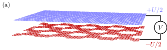
We consider a heterostructure consisting of a single layer of pristine graphene on top of a layer of GAL, as illustrated schematically in Fig. 1(a). The twist angle between the layers greatly influences the electronic properties of bilayer graphene, Lopes dos Santos et al. (2007); Lee et al. (2011) and we expect the properties of the proposed GOAL structures to also depend on the angle between the two layers. However, for simplicity we focus in this paper on perfect Bernal (AB) stacking of the two layers. We discuss the possible influence of the angle in more detail in the final section of the paper. Furthermore, experiments suggest the possibility of manually twisting the top layer until it ‘locks’ into place at the Bernal stacking angle. Dienwiebel et al. (2004)
Similar to the intricate edge dependence observed for graphene nanoribbons, Nakada et al. (1996) the exact shape of the antidot greatly influences the electronic properties of isolated GALs. In particular, extended regions of zigzag edges, which will generally be present for larger, circular holes, tend to induce quasi-localized states that significantly quench any present band gap. Gunst et al. (2011); Brun et al. (2014) To simplify the analysis of the proposed structures we focus on hexagonal holes with armchair edges. Experimental techniques exist that tend to favor the creation of specific edge geometries. Oberhuber et al. (2013); Jia et al. (2009); Pizzocchero et al. (2014); Xu et al. (2013) In addition to the hole shape, the orientation of the GAL superlattice with respect to the pristine graphene lattice has a profound impact on the electronic properties. Petersen et al. (2011); Brun et al. (2014) The orientation of a superlattice may be defined by the vectors between two neighboring antidots , where and are the lattice vectors of pristine graphene. It has been shown that if for any , the degeneracy at the Dirac point will break and a band gap is induced. Odom et al. (2000); Petersen et al. (2011); Ouyang et al. (2011) In this paper we consider GALs with two types of triangular superlattices: those with vectors parallel to carbon-carbon bonds which always induce a band gap, and those with vectors parallel to the pristine graphene lattice vectors which only induce gaps for a subset of superlattices. We only briefly discuss GOALs where the superlattice of the GAL layer is of the latter type, which we refer to as rotated GOALs and rotated GALs respectively, and focus mostly on the GAL superlattices for which band gaps are always present. We demonstrate below that GOALs containing gapped GAL layers display similar properties regardless of the superlattice type, whereas GOALs with non-gapped GAL layers essentially behave as bilayer graphene with a renormalized Fermi velocity.
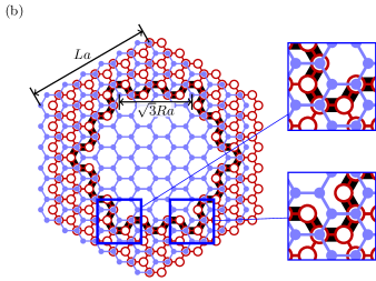
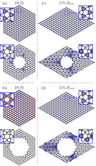
The Wigner–Seitz cell of a specific GOAL is illustrated in Fig. 1(b), where the red open circles represent the GAL layer atoms and the blue filled circles are the graphene layer atoms. To denote a given GOAL we use the notation , where is the side length of the hexagonal unit cell, while is the side length of the hexagonal hole in the GAL layer, with Å the graphene lattice constant. We use to refer to GOALs in which the isolated GAL layer is of the rotated type, as discussed above. Note that in this case, the Wigner–Seitz cell is not as shown in Fig. 1 but is rather in the shape of a rhombus with side length . Petersen et al. (2011) The condition for band gaps reads where for isolated rotated GALs and within our model the other two-thirds of the rotated GALs are gap-less. The superlattice constant of a GOAL is , while for a rotated GOAL it becomes .
In Bernal-stacked bilayer graphene there are four distinct sublattices, two in each layer. Within each layer we refer to these as dimer and non-dimer sites, and these sit directly above or below carbon sites (dimers) or the centers of hexagons (non-dimers) in the other layer. These sites are illustrated in the right of Fig. 1(b), where two of the antidot corners have been magnified. It has been shown that the low energy properties of bilayer graphene are dominated by non-dimer sites, and can be described using an effective two-band model with parabolic bands touching at the Fermi energy. McCann and Koshino (2013) The introduction of the hole, forming the GAL layer of the GOAL system results in a higher number of sites from each sublattice in the graphene layer than in the GAL layer, but within our model maintains the sublattice symmetry within each individual layer. The inter-layer asymmetry has important consequences when applying a bias across the layers, which we will discuss below in Sec. III.2. Furthermore, the structures of GOALs no longer display a rotational symmetry. Neighboring corners of a hexagonal hole are now associated with sites from opposite sublattices, as can be seen on the right of Fig. 1(b), reducing the symmetry of bilayer graphene to . Not all carbon sites in the graphene layer of a GOAL system are true dimers or non-dimers, as the respective sites or hexagons below may have been removed by the holes. However they still exhibit similar behavior to other sites in the same sublattice and we will thus collectively refer to them as dimers and non-dimers, respectively.
To calculate the electronic properties of the proposed structures, we use a nearest-neighbor tight-binding model. The low-energy properties of single-layer graphene are quite accurately described by a model taking into account just the nearest-neighbor hopping term, . For bilayer graphene, additional inter-layer hopping terms need to be included. We consider the Slonczewski–Weiss–McClure modelMcCann and Koshino (2013) with the direct intra-layer hopping term between AB dimers and the skew hopping terms and between dimers and non-dimers. As we show below in Sec. III, omitting the skew hopping terms has no qualitative impact on the results obtained. Therefore in most our calculations we disregard the skew hopping terms which are responsible for trigonal warping and electron-hole asymmetry in bilayer graphene. McCann and Koshino (2013) Furthermore, we do not include any on-site energy difference between dimer and non-dimer sites. McCann and Koshino (2013) The Hamiltonian then reads
| (1) |
where is the collection of nearest neighbor pairs within each layer and is the collection of dimer pairs. We take eV and eV.McCann and Koshino (2013); Kuzmenko et al. (2009) An inter-layer bias (initially ) can be included via a shift of the on-site energies on the GAL and the graphene layer, respectively. We define a positive bias to be one where the on-site energies of the graphene (GAL) layer are increased (decreased), as illustrated in Fig. 1(a).
III Electronic properties
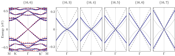
We begin by examining the electronic band structures of some GOAL systems in the absence of a transverse bias. The left-most panel of Fig. 2 shows the band structure of a GOAL. The GOALs all contain GAL layers with a triangular superlattice, which in their isolated form are gapped for all . The solid lines show the band structure calculated with intra-layer and direct inter-layer hoppings only, whereas the dashed lines show the results obtained when including also the skew hopping terms, eV and eV.McCann and Koshino (2013); Kuzmenko et al. (2009) The most striking features of the band structure are the linear bands near the Fermi energy, resembling the linear bands of single-layer graphene. The reduced Brillouin zone of the GOAL means that the and points of pristine graphene are folded onto the point. The most significant consequence of the skew hopping terms is to split the linear band into two linear bands with slightly different Fermi velocities. The band splitting and the difference in Fermi velocities becomes more pronounced in cases near pristine bilayer graphene, where the antidot size is relatively small. As we are mainly interested in a qualitative study of the proposed structures we disregard the skew hopping terms from hereon.
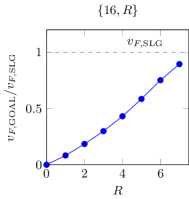
To illustrate the transition from the parabolic bands of bilayer graphene to the linear bands of single-layer graphene as the antidot size is increased, we show in the right panels of Fig. 2 the dispersion relation near the point for the GOALs with increasing values of . For comparison, the dashed (dotted) lines illustrate the pristine single-layer (bilayer) graphene dispersion, folded into the point. As the antidot size is increased, a transition from bilayer to single-layer-graphene-like (SLG-like) electronic properties is quite apparent, but with Fermi velocities which are slightly smaller than that of single-layer graphene. This transition is also clear from Fig. 3, which plots the Fermi velocity of the GOALs at as a function of . The transition towards SLG-like bands does not occur via an ever increasing curvature of two parabolic bands touching at the Fermi energy. Instead, we always observe a region of linear bands for , albeit the energy range in which the bands are linear is very narrow for small antidot sizes, and is accompanied by a strongly reduced Fermi velocity. Thus the low-energy band structure of GOAL can be considered as the crossing of two bands, similar to the case of single-layer graphene.
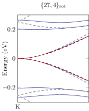
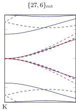
As the antidot size is increased more atoms are removed from the GAL layer and this leads to an effective reduction in the amount of bilayer graphene in the GOAL. We can quantify this via the relative area of bilayer graphene in the system, i.e. the ratio of the GAL and SLG layer areas, . It is reasonable to ask whether the cause of the transition from parabolic to linear bands is simply caused by a reduction in as is increased. To determine whether this is indeed the case, we show in Fig. 4 the band structures near the Dirac point for two GOALs, which consist of gapless rotated GAL layers. The superlattice constants of the and the corresponding GOALs are roughly similar () yielding very similar relative areas . The band structures for the two GOALs are shown in solid lines together with those of bilayer graphene in dashed gray lines. These rotated GOALs show a completely different dispersion, with no transition towards linear bands as the antidot size increases, even beyond the sizes shown in the figure. Despite having similar bilayer relative areas to the GOALs considered in Fig. 2, the band structures of the rotated GOALs remain parabolic and closely resemble that of pristine bilayer graphene.
We note that the isolated rotated GALs are gapless and that their band structures retain linear bands similar to pristine single-layer graphene, renormalized to a lower Fermi velocity. Petersen et al. (2011) This suggests that GOALs with gapless rotated GAL layers can be described by a model similar to that of bilayer graphene, but with a renormalized Fermi velocity. The low-energy dispersion of bilayer graphene is well described in a continuum model, McCann and Koshino (2013)
| (2) |
where is the Fermi velocity of single-layer graphene. To model the rotated GOAL we replace the Fermi velocity with the average Fermi velocity of the pristine graphene and renormalized GAL velocities, . The results of this simple model are illustrated by red dashed lines in Fig. 4, and indeed show quite good agreement with the full tight-binding results. Interestingly, rotated GOALs with gapped rotated GAL layers (e.g. , not shown) display no qualitative difference from the regular GOALs with gapped non-rotated GAL layers.
III.1 Distribution of states
The transition from parabolic to linear bands can thus not be explained entirely by the relative area of bilayer graphene, , in the GOAL system, but instead depends critically on the existence of a band gap in the isolated GAL layer. To illustrate how the band gap of the GAL layer induces the SLG-like behavior in the combined system we show the projected density of states (PDOS) at the Fermi energy for each layer of the and GOALs in Fig. 5(a) and (b). We will later discuss the differences in GOALs which consist of gapless GAL layers. The properties illustrated by the GOALs are qualitatively similar to those of . The PDOS of the two layers are displayed separately, with the graphene layer above and the GAL layer below. Furthermore, the PDOS of dimers and non-dimers are illustrated by filled red and blue circles, respectively. The size of the filled circles represents the value of the PDOS, which is normalized relative to that of pristine single-layer graphene shown by the open circles. The PDOS of the and GOALs are illustrated in Fig. 5(a) and (b), respectively. We recall that in the case of pristine single-layer (bilayer) graphene the Fermi energy density of states is equally distributed across all sites (all non-dimer sites). Examining first the graphene layers of the GOAL systems, we note that, unlike in bilayer graphene, there is a non-zero PDOS on dimer sites. Furthermore, this is equally distributed within the graphene layer, regardless of whether or not the sites are above another carbon site or above an antidot. Comparing the and cases, we see that the PDOS on dimer sites in the graphene layer increases with the antidot size. Meanwhile, the PDOS of the graphene layer non-dimers remains unchanged from that of single-layer graphene as the antidot size varies. Interestingly, in the GAL layer dimer PDOS remains zero for all antidot sizes. The PDOS of the non-dimer sites in the GAL layer displays a symmetry, yielding a three-fold symmetric confinement around antidot corners associated with non-dimer sites. Furthermore, the PDOS of the GAL layer non-dimers clearly decreases as the antidot size is increased. The net result of these features is that, for large antidots, the PDOS eventually displays a distribution largely confined in the graphene layer. This emerges from a decrease in the GAL layer non-dimer PDOS and an increase in that of the graphene layer dimer sites.
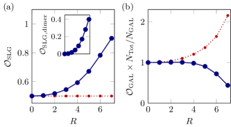
We can illustrate these findings more clearly by considering the PDOS integrated over all sites within each of the layers, which we quantify via the overlap
| (3) |
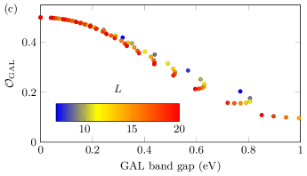
where is the expansion coefficient of the ’th eigenstate on to the -orbital centered at the ’th atomic site, and where denotes the layer, . A value of thus corresponds to an equal distribution of the eigenstates across both layers. The graphene layer localization at the Fermi energy is illustrated for GOALs in Fig. 6(a). The solid line in the figure shows the graphene layer overlap as a function of antidot size. As is increased the graphene layer overlap increases, i.e. the density of states become more confined in the graphene layer. The increased confinement is purely due to increased dimer PDOS, as apparent from the inset in Fig. 6(a) which displays the dimer overlap in the graphene layer, obtained by limiting the sum in Eq. (3) to dimer sites, as a function of antidot size. The increased graphene layer localization could be due to a simple redistribution of the density of states on to the remaining sites, where the overlap is proportional to the number of sites in the particular layer. We therefore consider the relative overlap , with denoting the total number of carbon atoms with , while the number of carbon atoms within the layer . The value thus denotes a GOAL with layer overlaps proportional to the number of sites in that particular layer. We show the relative overlap of the GOALs in Fig. 6(b). The solid line shows the relative overlap of the GAL layer as a function of the antidot size. The relative overlap is below unity for any non-zero and decreases with increasing antidot size. Thus the GAL layer confinement decreases more quickly than a simple redistribution can account for, pushing the density of states even further into the graphene layer. This transition from bilayer to single-layer confinement is critically dependent on the GAL band gap, and we therefore illustrate the GAL layer overlap for various GOALs as a function of the isolated GAL gap in Fig. 6(c). Each GOAL is represented by a point colored by the value of . We find that the overlap in the GAL layer decreases with the GAL band gap in a largely one-to-one correlation, except at high GAL band gaps obtained through rather impractical antidot lattices, e.g. where the distance between antidots is only slightly larger than the antidot size. As the GAL band gap increases states are pushed out of the GAL layer and into the graphene layer, effectively localizing the states in a single-layer yielding the SLG-like behavior. This occurs, as we saw in Fig. 5, via a transfer of states between the GAL layer non-dimer and graphene layer dimer sites as the antidot size, and thus the band gap, is increased.
To further illustrate the importance of the GAL band gap, we now consider the rotated GOALs which consist of gapless GAL layers and display a renormalized bilayer-like dispersion. The PDOS at for the and GOALs are illustrated in Fig. 5(c) and (d), respectively. The most notable feature in the rotated GOAL systems, as opposed to the non-rotated GOALs, is the zero PDOS of dimer sites in both layers of the rotated GOALs. The PDOS of the non-dimer sites in the graphene layer remains unaffected by the introduction of an antidot and the increasing of . Therefore, the PDOS of the GAL layer non-dimer sites must increase. This is more clearly seen in Fig. 6(a) where the graphene layer overlap of the GOALs is illustrated by the dotted red line. As the antidot size increases, no changes occur in the overlap of the graphene layer and hence also not in the overlap of the GAL layer. In Fig. 6(b) we display the relative overlap of the GAL layer of the by the dotted red line. In these rotated GOALs, the relative overlap increases above unity, corresponding to the redistribution of the PDOS onto the remaining non-dimer sites within the GAL layer. This is also seen in the GAL layers of the GOALs shown in right panels of Fig. 5, where the PDOS of the individual non-dimer sites has been significantly increased compared to the GOALs. GOALs with gapless GAL layers do not push states into the graphene layer, but instead simply redistribute the density of states in the non-dimer sites of the GAL layer. A low energy distribution of states amongst non-dimer sites only is a noted property of bilayer graphene, and confirms again the relation between the properties of rotated GOALs and those of the pristine bilayer. We limit the remainder of this paper to an investigation of the non-rotated GOALs, where the migration of states from the GAL to the graphene layer leads to an even distribution of states amongst the sublattices of the graphene layer, and thus to SLG-like behavior.
III.2 Bias-tunable band gaps
We now turn to biased structures. A potential difference between the layers induces a band gap in the case of pristine bilayer graphene, the size of which can be tuned by the bias voltage. McCann and Koshino (2013); Nilsson et al. (2007); Castro et al. (2010); Ohta et al. (2006) The potential can be created by a uniform electric field perpendicular to the two layers. In experimental systems the voltage difference is an induced quantity from the larger applied potential that due to screening and interlayer coupling is significantly reduced. For bilayer graphene the potential is uniform within the two layers and the induced voltage difference can be assumed linearly proportional to the applied voltage , in which case currently has been predicted to realistically lie between 0.3 eV. Nilsson et al. (2007) We note that in GOAL the edges will likely induce an inhomogeneous potential distribution. To find this distribution requires a self-consistent solution to the Poisson equation and band structure, a level of complication beyond the current scope. We limit our model to include the bias via a uniformly distributed on-site energy shift for the graphene and GAL layers respectively.
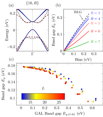
In a biased GOAL system, the inter-layer asymmetry of the on-site energies opens a band gap around the Dirac point. We illustrate this in Fig. 7(a) through the band structures of two biased GOALs at eV. In this figure, the bands of biased and GOALs are shown in dashed red and solid blue lines respectively, together with the bands of pristine biased bilayer graphene in dotted gray lines. The band gap of biased GOAL is smaller than that of biased bilayer graphene or of the smaller antidot GOAL. The change of the gap size is quantified in Fig. 7(b) where we illustrate the band gaps of several biased GOALs as a function of . Each GOAL is shown as a solid line colored according to the value of . Additionally, the band gap of biased bilayer graphene is shown as a dashed line. The band structures of the two biased GOALs in Fig. 7(a) further display electron-hole asymmetry. This arises due to the atomic imbalance between the two layers combined with the equal but opposite on-site energy shifts used to model the bias. While the effect is minor in case of small antidots, for larger antidots the net energy shift caused by the imbalanced bias distribution yields a valence band shifted towards . We note also that the band structure of the biased GOAL resembles that of gapped graphene, identified by the absence of the “Mexican hat” profile of biased bilayer graphene McCann and Koshino (2013). The absence of the flat profiles of biased bilayer graphene yields larger group velocities, which in turn is very attractive in fast electronic applications. The transition between the bilayer graphene and gapped SLG-like dispersion is smooth, and similar to the zero-bias case can not be contributed solely to the reduced area . To illustrate this, we plot the biased GOAL band gap dependence on the isolated GAL gap for various GOALs in Fig. 7(c) at eV, where each GOAL is represented by a point colored by the value of . The figure demonstrates clearly that an increase in the isolated GAL gap will cause a decrease of the biased GOAL band gap. Although perhaps counterintuitive, this behavior is the direct result of GOALs with large band gap GAL layers exhibiting graphene layer confinement. This effectively reduces the inter-layer asymmetry felt by the electronic states and reduces the band gap of the combined structure. Fig. 7(c) displays a clear correlation between the GAL band gap and the biased GOAL band gap, though it does display increased spreading as the GAL band gap is increased. This spreading signifies an additional complication due to the uniform on-site energy shift in the two asymmetric layers. While the largest band gaps are found for GOAL systems whose unbiased electronic structure most closely resembles that of bilayer graphene, there is a range of values that yield both sizable band gaps and largely linear dispersion relations, e.g. the shown here and also the case. This presents the interesting possibility of combining high Fermi velocity electronic transport similar to single-layer graphene with a gate-controllable band gap.
IV Transport properties
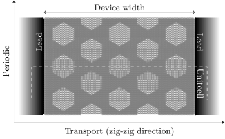
We mentioned two ways of experimentally fabricating GOAL devices; either by single-layer etching bilayer graphene or stacking a graphene sheet onto a GAL sheet. Most experimental transport measurements in bilayer graphene have been performed with top-contacts to inject current, and using dual-gates to control the inter-layer bias. Oostinga et al. (2008); Du et al. (2008); Weitz et al. (2010) With recent advances in side-contacts, first in single-layer graphene Wang et al. (2013) and then in bilayer graphene Maher et al. (2014), there are now several ways of injecting current into a bilayer material such as GOAL. The consequence of the choice of contacts has been studied for pristine bilayer graphene ribbons and flakes. González et al. (2010, 2011) To illustrate the consequences of the choice of contacts, we consider the electronic transport through a finite-width strip of GOAL. To calculate the transport properties, we employ the Landauer-Büttiker formalism. The transport is calculated between two leads composed of either single- or bilayer graphene. A schematic illustration of the transport model is shown in Fig. 8. In case of bilayer leads, these are connected to both the graphene and GAL layers, while single-layer leads are coupled to either the graphene or the GAL layer. Both the leads and the device are periodic in the transverse direction, and the unit cell used in calculations is outlined by the dashed rectangle. We consider transport in the zig-zag-direction. This yields a dense cross-section of antidots, effectively reducing the width of the GOAL device needed to represent large-width GOAL transport. Gunst et al. (2011) Our calculations are performed on strips of GOAL with 7 antidots rows present along the transport direction. This width yields a well defined transport gap in the isolated GAL layer. Gunst et al. (2011)
With respect to the Landauer-Büttiker formula , the transmission is determined using the Fisher-Lee relation which couples the transport to the Green’s function of the full system. Lewenkopf and Mucciolo (2013); Datta (1995) The two leads are accounted for in the central device through the left () and right () self-energies and . The retarded Green’s function at energy then reads
| (4) |
where is the isolated Hamiltonian of the device region and is a small imaginary parameter needed for numerical stability. Finally, the transmission is determined using the relation
| (5) |
where the are the line widths for the respective leads. Bond currents through the device at specific energies are useful quantities in establishing how current flows through different parts of the device. Lewenkopf and Mucciolo (2013) The current between two neighboring sites and at the energy is Cresti et al. (2003)
| (6) |
where is the hopping term between the sites and . The transport calculations use both approximative recursive Green’s function techniques to determine the lead self-energies and exact techniques for the device region to significantly speed up calculations, following Ref. 63.
IV.1 Transmission
We consider two illustrative examples, the and GOALs. From previous sections we recall that the and GOALs exhibit bilayer-like and single-layer-like dispersions, respectively.
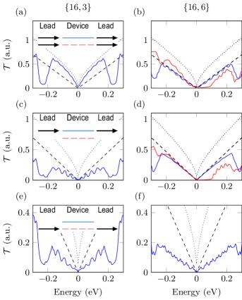
The transmissions between bilayer graphene leads connected to the and the GOAL devices are shown by solid blue lines in Fig. 9(a) and (b), respectively. These transmissions are compared with pristine single- and bilayer graphene transmission, shown by dashed black and dotted gray lines, respectively. Close to the Fermi energy, the transmission of the GOAL appears very similar to the pristine bilayer case, but with a slightly smaller magnitude. This is consistent with the bilayer-like dispersion of the GOAL. In contrast, the GOAL transmission appears very similar to that of single-layer graphene. The qualitative transition from bilayer-like to single-layer-like transport behavior as a function of isolated GAL band gap is similar to that previously noted for the band dispersion. Furthermore, an oscillatory behavior is observed which is particularly apparent for the transmission. By increasing the number of antidot rows beyond 7 (not shown) the transmissions yield an increased oscillation frequency, suggesting a Fabry-Perot like interference between scatterings at the lead-device interfaces. The low transmission valleys just above eV, which are present for both GOALs, appear at the end of the linear dispersion region and the onset of higher order bands.
The transmission between single-layer graphene leads coupled to the graphene layer of the GOALs is shown in Fig. 9(c) and (d) (solid blue lines), compared again to pristine single- and bilayer graphene transmission (dashed black and dotted gray lines, respectively). The transmission through the graphene layer of the GOAL is much lower than single-layer graphene transmission. This generally occurs for GOALs containing small-gap GAL layers due to wave mismatching, where the single-layer nature of the incoming wave is mismatched with the propagating bilayer waves in the GOAL device. We note that this also occurs in cases of bilayer graphene leads coupled to extremely large GAL gapped GOALs e.g. like where the incoming bilayer wave is mismatched with the single-layer nature of the GOAL device. However, in the GOAL the layers are sufficiently decoupled to have single-layer-like propagating states, thus yielding a single-layer-like transmission. Likewise, the Fabry-Perot oscillations have disappeared signifying lowered interface scattering, while they remain for the GOAL. The transmission between single-layer leads coupled to the GAL layer of and GOALs is shown in Fig. 9(e) and (f), respectively. In this case the transmissions for both GOAL devices are lower than that of single-layer graphene. The current must flow through either the GAL layer or couple in to and out of the graphene layer, which limits the transmission by the GAL band gap or the inter-layer couplings.
Finally, we consider the GOAL devices with an applied bias of eV. The single layer and bilayer contact transmissions are illustrated in Fig. 9(b) and (d) by red solid lines. The band gap of the GOAL system forms a corresponding transport gap, effectively providing a SLG-like material with a tunable transport gap. The optimal configuration for injecting current into a GOAL-based device should contact both layers, e.g. a side-contacted device.
IV.2 Bond currents
In order to clarify the single-layer-like transport of GOALs, we now examine the bond currents in the systems studied above. We distinguish between in-plane and out-of-plane currents; currents flowing within either layer or currents flowing between the layers, respectively. The model is the same as for the transmission illustrated in Fig. 8, where semi-infinite leads are coupled to a central GOAL device.
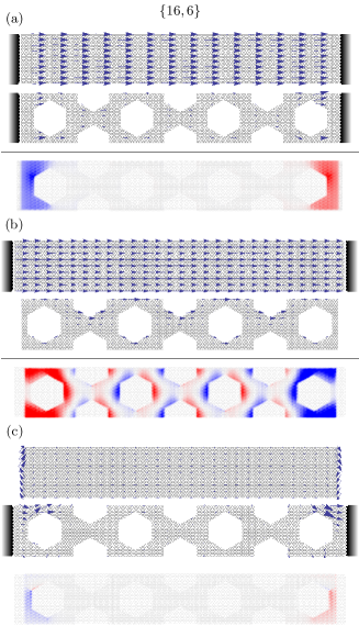
We consider the two cases where GOAL devices displayed transmissions similar to single-layer graphene, i.e. the GOAL device connected to either bilayer graphene leads or single-layer graphene leads which couple to the graphene layer only. We illustrate current maps of the GOAL device at the energy eV in Fig. 10. In Fig. 10(a) the currents of the GOAL device coupled to the bilayer leads is shown. We plot the in-plane currents in each layer of the GOAL device separately, and show those of the graphene layer above those of the GAL layer. These currents are displayed as vector maps, which are scaled relative to the maximum current in both layers. The most notable feature of the in-plane currents of the GOAL device with bilayer leads is the confinement of the current to the graphene layer throughout most of the device. The out-of-plane current components are shown below the in-plane components as normalized color maps. Blue shading represents for current flow from the GAL layer to the graphene layer, whilst red represents current from graphene layer to GAL layer. This map displays a large current entering the graphene layer at the left interface and leaving at the right, yielding largely single-layer current transport. The current within the GAL layer is not zero, and as the energy is increased the current within the GAL layer increases in magnitude. The current thus becomes more and more bilayer-like as the energy of transport in increased, consistent with moving away from the band gap of the GAL layer. In Fig. 10(b) the bond currents in the GOAL device with a graphene layer connection to the single-layer leads are shown. The in plane currents in this case also display noticeable confinement in the graphene layer. However, in this case we observe that the in-plane current within the GAL layer is significantly larger. The out-of-plane current map suggests the the current flows to the GAL layer near the left electrode and oscillates between the two layers near antidot edges, before returning to the graphene layer at the right electrode. In both of these transport configurations, the current is largely confined to the graphene layer, yielding a transmission similar to, but slightly smaller than, single-layer transport.
Another interesting behavior occurs in the final case of single-layer leads connected to the GAL layer, illustrated in Fig. 10(c). In this case, the transport currents in a GOAL exhibit large edge currents within the graphene layer along the transverse (periodic) direction. This behavior is a consequence of the high localization at every other corner in the hexagonal antidots, see Fig. 5, such that the zigzag transport-direction will always scatter the current asymmetrically along the transverse direction. If the same calculation is done along the armchair transport-direction, the scattering at the corners is symmetric and one finds much smaller and symmetric transverse currents. Even though the transmission here is far smaller than single-layer graphene transport, the high transverse currents induced in the graphene layer suggest that interesting inter-layer transport couplings may be possible.
V Discussion and Conclusion
In this work we have studied the electronic and transport properties of an all-carbon bilayer heterostructure consisting of a layer of pristine graphene atop a layer of nanostructured graphene. In order to determine the general properties of such a heterostructure, we considered antidots as the ideal testbed, where structurally similar configurations yield entirely different single-layer properties. These antidots were arranged into a triangular, or rotated triangular, superlattice orientation, yielding respectively gapped and gap-less antidot layers. The electronic properties of the unbiased composite GOAL structures were seen to depend critically on the existence of this band gap in the isolated GAL layer. A gapped GAL layer, regardless of superlattice orientation, will push electronic states into the graphene layer. This is evident from the graphene layer confinement of the density of states, shown in Fig. 6(c), which increases with the GAL band gap. As a consequence, the sublattice distribution of states seen in bilayer graphene is broken. Instead we find an approximately even distribution of states between sublattices in the graphene layer, i.e. dimers as well as non-dimers. Upon increasing the graphene layer confinement, the GOAL dispersion becomes linear near the Dirac point, and furthermore, the Fermi velocity increases until (at high GAL band gaps) it resembles that of pristine single-layer graphene. Conversely, if the isolated GAL layer does not contain a gap, the GOAL composite retains a bilayer-like dispersion, except for a slight renormalization of the Fermi velocity. The electronic state distribution in such GOALs is unchanged in the graphene layer, i.e. entirely located on non-dimers, while it is redistributed amongst the remaining sites in the GAL layer in a manner that conserves the pristine bilayer sublattice asymmetry. The dependence on the gap, and not directly the superlattice orientation or dimension, suggests a generality beyond this particular heterostructure.
Introducing an inter-layer bias to the GOALs with single-layer like dispersion induces band gaps smaller than those predicted for pristine bilayer graphene. The GOAL band gap size decreases as the band gap of its associated isolated GAL layer is increased. While GOALs with large-gap GAL layers have significantly reduced band gaps in the combined GOAL systems, specific GOAL structures were seen to exhibit both SLG-like dispersion and a sizable, tunable band gap. Certain structures, such as the and GOALs, were identified which retained a high Fermi velocity in the unbiased case and sizable band gap in the biased case. Additionally, these GOAL systems when biased display gapped graphene-like bands, as opposed to the “Mexican hat” shape bands of bilayer graphene. The consequence is higher electron velocities than those in regular gapped bilayer graphene, which is of great interest in high-speed electronics. Introducing a band gap in bilayer systems has been successfully done in experiments, Ohta et al. (2006); Castro et al. (2007); Oostinga et al. (2008) and our results suggest a possibility of manipulating and fine tuning similar electronic behavior by nanostructuring of one of the layers.
In this work, we have limited our study to Bernal-stacked GOAL systems and to the most important coupling parameters, the intra-layer hopping and inter-layer hopping . Nonetheless, we expect more elaborate models to show the same qualitative results. The inclusion of additional inter-layer couplings, responsible for electron-hole asymmetry and trigonal warping, McCann and Koshino (2013) causes only a minor splitting of the bands near the Dirac point into two separate linear bands with slightly different Fermi velocities. While this effect is more pronounced in GOALs with gap-less or smaller gap GAL layers, our focus is mainly on the more interesting single-layer-like GOALs with larger gap GAL layers. It would however be very interesting to verify or modify these parameters through the use of ab initio calculations specifically for GOALs. Additionally, we employ a simple uniform potential distribution to describe the bias, which neglects edge effects that are likely to arise in these structures. Given the intricate edge distribution of the density of states, the correct potential distribution may induce changes in the band edges of biased GOALs. We also do not employ disorder or twisting of the GOAL systems. In the case of disorder, this tends to decrease the band gap on an isolated GAL system. The dispersion of the corresponding GOALs may exhibit transitions towards bilayer-like dispersion. However, antidots with a hexagonal armchair shapes display higher stability against disorder than circular or hexagons with extended zigzag-edges. Power and Jauho (2014) By using experimental methods that prefer armchair edged shapes, this transition can be limited. In case of twisting, models have been developed to illustrate what effect a small-angle twist has on the electronic properties in pristine twisted bilayer graphene.Lopes dos Santos et al. (2007, 2012) Depending on the angle, the dispersion relations of twisted bilayers range from the parabolic bands of Bernal-stacked bilayer graphene to linear bands with a low Fermi velocity. Lopes dos Santos et al. (2012) In the case of GOAL-based systems, the effect might be similar i.e. decreasing the Fermi velocity. Furthermore, when the twisted bilayer graphene dispersion becomes linear the application of a perpendicular electric field is no longer guaranteed to open a band gap. Lopes dos Santos et al. (2007) As such, the inclusion of a twist angle would require a more extensive study.
We have also studied transport properties including different contact configurations. The transmission through GOALs exhibiting single-layer-like dispersion has approximatively the same magnitude as transmission through pristine graphene. Furthermore, the current flow was largely confined to the graphene layer of the GOAL. This follows from the electronic transport in pristine biased bilayer graphene, which depends greatly on the sublattice balances of the system. The current density is greatest in the layer where the charge density is distributed equally across nondimers and dimers. Páez et al. (2014) The transport properties of GOALs also depend greatly on the type of contact to the device, similar to the case of pristine bilayer graphene. González et al. (2010, 2011) As the GOALs are bilayer materials, their propagating waves are also usually bilayer, albeit largely confined in the graphene layer. This holds true except at very large GAL band gaps. As such, GOALs display the highest transmission when coupling to bilayer graphene leads. Unlike isolated GAL devices, the GAL layer of a GOAL device does not act as a barrier for transport. Instead, the graphene-like transmission should be viewed as a result of mostly single-layer confinement of the propagating states. Coupling from single-layer leads, the mismatch between the incoming single-layer states and bilayer-like device states gives rise to increased interface scattering. Except for very large GAL band gaps, this leads to transmissions below that of single-layer graphene. The transmissions through GOAL devices with large-gapped GAL layers resemble that of SLG, suggesting single-layer-like propagation states. In contrast to this, where single-layer leads connect only to the GAL layer the transmission is always low. Both the lead/device wave mismatch and the current flow between the layers lead to the reduced transmission. Furthermore, in these cases the transport can display significant transverse currents within the graphene layer due to asymmetric scattering at hole edges. For realistic devices, the best transmission is gained by injecting current into both layers, e.g. a side contact.
In this study we have demonstrated that the bilayer heterostructure can exhibit single-layer-like behavior similar to that of pristine graphene, while still allowing a tunable band gap. The bilayers in this paper are seen to display a critical dependence on the band gap within the nanostructured layer. All results suggest that, as this band gap is increased the electronic states localize in the pristine layer, which yields monolayer behavior. From this, we expect that such a bilayer, with a gapless and a gapped layer, will transition from monolayer to bilayer behavior as the band gap within the gapped layer decreases. Modifications which decrease such a gap may include structural defects, disorder and other imperfections, which in turn would lead to more bilayer-like behavior. Many of the features discussed in this work may also be of relevance to other instances of 2D heterostructures where a metallic or semimetallic layer is coupled to a semiconducting or insulating layer. We expect that in these cases a similar interplay between the electronic properties of the individual layers, and the redistribution of states when they are stacked, will determine the electronic and transport properties. Such similar bilayer systems could include other forms of patterning of the nanostructured e.g. with dopants, Jin et al. (2011); Guillaume et al. (2012); Samuels and Carey (2013); Mao et al. (2010) absorbants, Balog et al. (2010); Collado et al. (2015); Felten et al. (2013) or a Moiré potentials arising from coupling to a substrate. Giovannetti et al. (2007) Given the intense research currently underway in the field of nanostructured graphene, and the recent experimental progress in 2D heterostructure stacking, we believe that this type of composite system could bring interesting possibilities yet unseen in pristine graphene systems.
VI Acknowledgments
We thank Thomas Garm Pedersen for a fruitful discussion. The Center for Nanostructured Graphene (CNG) is sponsored by the Danish Research Foundation, Project DNRF58. The work by J.G.P. is financially supported by the Danish Council for Independent Research, FTP Grants No. 11-105204 and No. 11-120941.
References
- Geim and Novoselov (2007) A. K. Geim and K. S. Novoselov, Nature materials 6, 183 (2007).
- Castro Neto et al. (2009) A. H. Castro Neto, N. M. R. Peres, K. S. Novoselov, and A. K. Geim, Reviews of Modern Physics 81, 109 (2009).
- Xia et al. (2010) F. Xia, D. B. Farmer, Y.-M. Lin, and P. Avouris, Nano letters 10, 715 (2010).
- Schwierz (2013) F. Schwierz, Proceedings of the IEEE 101, 1567 (2013).
- Schwierz (2010) F. Schwierz, Nature nanotechnology 5, 487 (2010).
- Han et al. (2007) M. Y. Han, B. Özyilmaz, Y. Zhang, and P. Kim, Physical Review Letters 98, 206805 (2007).
- Nakada et al. (1996) K. Nakada, M. Fujita, G. Dresselhaus, and M. S. Dresselhaus, Physical Review B 54, 17954 (1996).
- Brey and Fertig (2006) L. Brey and H. A. Fertig, Physical Review B 73, 235411 (2006).
- Ezawa (2006) M. Ezawa, Physical Review B 73, 045432 (2006).
- Pereira et al. (2009) V. M. Pereira, A. H. Castro Neto, and N. M. R. Peres, Physical Review B 80, 045401 (2009).
- Pereira and Castro Neto (2009) V. M. Pereira and A. H. Castro Neto, Physical Review Letters 103, 046801 (2009).
- Pedersen and Pedersen (2012) J. G. Pedersen and T. G. Pedersen, Physical Review B 85, 235432 (2012).
- Low et al. (2011) T. Low, F. Guinea, and M. I. Katsnelson, Physical Review B 83, 195436 (2011).
- Neek-Amal et al. (2012) M. Neek-Amal, L. Covaci, and F. M. Peeters, Physical Review B 86, 041405 (2012).
- Balog et al. (2010) R. Balog, B. Jørgensen, L. Nilsson, M. Andersen, E. Rienks, M. Bianchi, M. Fanetti, E. Laegsgaard, A. Baraldi, S. Lizzit, Z. Sljivancanin, F. Besenbacher, B. Hammer, T. G. Pedersen, P. Hofmann, and L. Hornekaer, Nature materials 9, 315 (2010).
- Denis (2010) P. A. Denis, Chemical Physics Letters 492, 251 (2010).
- Pedersen et al. (2008) T. G. Pedersen, C. Flindt, J. G. Pedersen, N. A. Mortensen, A.-P. Jauho, and K. Pedersen, Physical Review Letters 100, 136804 (2008).
- Petersen et al. (2011) R. Petersen, T. G. Pedersen, and A.-P. Jauho, ACS nano 5, 523 (2011).
- Pedersen et al. (2012) J. G. Pedersen, T. Gunst, T. Markussen, and T. G. Pedersen, Physical Review B 86, 245410 (2012).
- Gunst et al. (2011) T. Gunst, T. Markussen, A.-P. Jauho, and M. Brandbyge, Physical Review B 84, 155449 (2011).
- Brun et al. (2014) S. J. Brun, M. R. Thomsen, and T. G. Pedersen, Journal of physics. Condensed matter : an Institute of Physics journal 26, 265301 (2014).
- Thomsen et al. (2014) M. R. Thomsen, S. J. Brun, and T. G. Pedersen, Journal of physics. Condensed matter : an Institute of Physics journal 26, 335301 (2014).
- Yuan et al. (2013) S. Yuan, R. Roldán, A.-P. Jauho, and M. I. Katsnelson, Physical Review B 87, 085430 (2013).
- Power and Jauho (2014) S. R. Power and A.-P. Jauho, Physical Review B 90, 115408 (2014).
- Kim et al. (2010) M. Kim, N. S. Safron, E. Han, M. S. Arnold, and P. Gopalan, Nano letters 10, 1125 (2010).
- Kim et al. (2012) M. Kim, N. S. Safron, E. Han, M. S. Arnold, and P. Gopalan, ACS nano 6, 9846 (2012).
- Oberhuber et al. (2013) F. Oberhuber, S. Blien, S. Heydrich, F. Yaghobian, T. Korn, C. Schüller, C. Strunk, D. Weiss, and J. Eroms, Applied Physics Letters 103, 143111 (2013).
- Giesbers et al. (2012) A. J. M. Giesbers, E. C. Peters, M. Burghard, and K. Kern, Physical Review B 86, 045445 (2012).
- Eroms and Weiss (2009) J. Eroms and D. Weiss, New Journal of Physics 11, 095021 (2009).
- Shen et al. (2008) T. Shen, Y. Q. Wu, M. A. Capano, L. P. Rokhinson, L. W. Engel, and P. D. Ye, Applied Physics Letters 93, 122102 (2008).
- Bai et al. (2010) J. Bai, X. Zhong, S. Jiang, Y. Huang, and X. Duan, Nature nanotechnology 5, 190 (2010).
- Xu et al. (2013) Q. Xu, M.-Y. Wu, G. F. Schneider, L. Houben, S. K. Malladi, C. Dekker, E. Yucelen, R. E. Dunin-Borkowski, and H. W. Zandbergen, ACS nano 7, 1566 (2013).
- Castro et al. (2010) E. V. Castro, K. S. Novoselov, S. V. Morozov, N. M. R. Peres, J. M. B. Lopes dos Santos, J. Nilsson, F. Guinea, A. K. Geim, and A. H. Castro Neto, Journal of physics. Condensed matter 22, 175503 (2010).
- Lopes dos Santos et al. (2007) J. M. B. Lopes dos Santos, N. M. R. Peres, and A. H. Castro Neto, Physical Review Letters 99, 256802 (2007).
- McCann and Koshino (2013) E. McCann and M. Koshino, Reports on Progress in Physics 76, 56503 (2013).
- Ohta et al. (2006) T. Ohta, A. Bostwick, T. Seyller, K. Horn, and E. Rotenberg, Science 313, 951 (2006).
- Páez et al. (2014) C. J. Páez, D. a. Bahamon, and A. L. C. Pereira, Physical Review B 90, 125426 (2014).
- Zhang et al. (2009) Y. Zhang, T.-T. Tang, C. Girit, Z. Hao, M. C. Martin, A. Zettl, M. F. Crommie, Y. R. Shen, and F. Wang, Nature 459, 820 (2009).
- Barbier et al. (2010) M. Barbier, P. Vasilopoulos, and F. M. Peeters, Philosophical transactions. Series A, Mathematical, physical, and engineering sciences 368, 5499 (2010).
- Kvashnin et al. (2014) D. G. Kvashnin, P. Vancsó, L. Y. Antipina, G. I. Márk, L. P. Biró, P. B. Sorokin, and L. A. Chernozatonskii, Nano Research 1, 1 (2014).
- Killi et al. (2011) M. Killi, S. Wu, and A. Paramekanti, Physical Review Letters 107, 086801 (2011).
- Guillaume et al. (2012) S. O. Guillaume, B. Zheng, J. C. Charlier, and L. Henrard, Physical Review B - Condensed Matter and Materials Physics 85, 1 (2012).
- Samuels and Carey (2013) A. J. Samuels and J. D. Carey, ACS Nano 7, 2790 (2013).
- Mao et al. (2010) Y. Mao, G. Malcolm Stocks, and J. Zhong, New Journal of Physics 12 (2010), 10.1088/1367-2630/12/3/033046.
- Collado et al. (2015) H. P. O. Collado, G. Usaj, and C. A. Balseiro, 045435, 1 (2015).
- Felten et al. (2013) A. Felten, B. S. Flavel, L. Britnell, A. Eckmann, P. Louette, J. J. Pireaux, M. Hirtz, R. Krupke, and C. Casiraghi, Small 9, 631 (2013).
- Geim and Grigorieva (2013) A. K. Geim and I. V. Grigorieva, Nature 499, 419 (2013).
- Lee et al. (2011) D. S. Lee, C. Riedl, T. Beringer, A. H. Castro Neto, K. von Klitzing, U. Starke, and J. H. Smet, Physical Review Letters 107, 216602 (2011).
- Dienwiebel et al. (2004) M. Dienwiebel, G. S. Verhoeven, N. Pradeep, J. W. M. Frenken, J. A. Heimberg, and H. W. Zandbergen, Physical Review Letters 92, 126101 (2004).
- Jia et al. (2009) X. Jia, M. Hofmann, V. Meunier, B. G. Sumpter, J. Campos-Delgado, J. M. Romo-Herrera, H. Son, Y.-P. Hsieh, A. Reina, J. Kong, M. Terrones, and M. S. Dresselhaus, Science 323, 1701 (2009).
- Pizzocchero et al. (2014) F. Pizzocchero, M. Vanin, J. Kling, T. W. Hansen, K. W. Jacobsen, P. Bøggild, and T. J. Booth, The Journal of Physical Chemistry C 118, 4296 (2014).
- Odom et al. (2000) T. W. Odom, J.-L. Huang, P. Kim, and C. M. Lieber, The Journal of Physical Chemistry B 104, 2794 (2000).
- Ouyang et al. (2011) F. Ouyang, S. Peng, Z. Liu, and Z. Liu, ACS nano 5, 4023 (2011).
- Kuzmenko et al. (2009) A. B. Kuzmenko, I. Crassee, D. van der Marel, P. Blake, and K. S. Novoselov, Physical Review B 80, 165406 (2009).
- Nilsson et al. (2007) J. Nilsson, A. H. Castro Neto, F. Guinea, and N. M. R. Peres, Physical Review B 76, 165416 (2007).
- Oostinga et al. (2008) J. B. Oostinga, H. B. Heersche, X. Liu, A. F. Morpurgo, and L. M. K. Vandersypen, Nature materials 7, 151 (2008).
- Du et al. (2008) X. Du, I. Skachko, A. Barker, and E. Y. Andrei, Nature nanotechnology 3, 491 (2008).
- Weitz et al. (2010) R. T. Weitz, M. T. Allen, B. E. Feldman, J. Martin, and A. Yacoby, Science 330, 812 (2010).
- Wang et al. (2013) L. Wang, I. Meric, P. Y. Huang, Q. Gao, Y. Gao, H. Tran, T. Taniguchi, K. Watanabe, L. M. Campos, D. a. Muller, J. Guo, P. Kim, J. Hone, K. L. Shepard, and C. R. Dean, Science 342, 614 (2013).
- Maher et al. (2014) P. Maher, L. Wang, Y. Gao, C. Forsythe, T. Taniguchi, K. Watanabe, D. Abanin, Z. Papić, P. Cadden-Zimansky, J. Hone, P. Kim, and C. R. Dean, Science 345, 61 (2014).
- González et al. (2010) J. W. González, H. Santos, M. Pacheco, L. Chico, and L. Brey, Physical Review B 81, 195406 (2010).
- González et al. (2011) J. W. González, H. Santos, E. Prada, L. Brey, and L. Chico, Physical Review B 83, 205402 (2011).
- Lewenkopf and Mucciolo (2013) C. H. Lewenkopf and E. R. Mucciolo, Journal of Computational Electronics 12, 203 (2013).
- Datta (1995) S. Datta, Electronic Transport in Mesoscopic Systems, 3rd ed. (Cambridge University Press, Cambridge, 1995).
- Cresti et al. (2003) A. Cresti, R. Farchioni, G. Grosso, and G. P. Parravicini, Physical Review B 68, 075306 (2003).
- Castro et al. (2007) E. Castro, K. Novoselov, S. Morozov, N. Peres, J. dos Santos, J. Nilsson, F. Guinea, A. K. Geim, and A. Neto, Physical Review Letters 99, 216802 (2007).
- Lopes dos Santos et al. (2012) J. M. B. Lopes dos Santos, N. M. R. Peres, and A. H. Castro Neto, Physical Review B 86, 155449 (2012).
- Jin et al. (2011) Z. Jin, J. Yao, C. Kittrell, and J. M. Tour, ACS nano 5, 4112 (2011).
- Giovannetti et al. (2007) G. Giovannetti, P. Khomyakov, G. Brocks, P. Kelly, and J. van den Brink, Physical Review B 76, 073103 (2007).