Anisotropic strain in SmSe and SmTe: implications for electronic transport
Abstract
Mixed valence rare-earth samarium compounds SmX (X=Se,Te) have been recently proposed as candidate materials for use in high-speed, low-power digital switches driven by stress induced changes of resistivity. At room temperature these materials exhibit a pressure driven insulator-to-metal transition with resistivity decreasing by up to 7 orders of magnitude over a small pressure range. Thus, the application of only a few GPa’s to the piezoresistor (SmX) allows the switching device to perform complex logic. Here we study from first principles the electronic properties of these compounds under uniaxial strain and discuss the consequences on carrier transport. The changes in the band structure show that the piezoresistive response is mostly governed by the reduction of band gap with strain. Furthermore, it becomes optimal when the Fermi level is pinned near the localized valence band. The piezoresistive effect under uniaxial strain which must be taken into account in thin films and other systems with reduced dimensionality is also quantified. Under uniaxial strain we find that the piezoresistive response can be substantially larger than in the isotropic case. Analysis of complex band structure of SmSe yields a tunneling length of the order of 1 nm. The results suggest that the conduction mechanism governing the piezoresistive effect in bulk, i.e. thermal promotion of electrons, should still be dominant in few-nanometer-thick films.
I Introduction
There is currently great interest in novel electronic switches for use in post-CMOS logic Theis and Solomon (2010). Recently, a new high performance computer switch has been proposed promising high speed at low power Newns et al. (2012a). The switch operates through the use of a nanoscale piezoelectric actuator applying uniaxial stress to a piezoresistive element. The piezoresistive material undergoes an insulator to metal transition thereby turning the device on. The device can be described as a type of nano-electro-mechanical system (NEMS) device wherein all the parts stay in continuous mechanical contact.
In order to form an effective device, the piezoelectric and the piezoresistor must exhibit high performance. Here we concentrate on the piezoresistor which must have high sensitivity to applied strain (large resistance drop, , with little applied stress), fast response to the applied stress and high endurance to cycling. These requirements define the engineering envelope for effective piezoresistive materials in logic devices Barlian et al. (2009). For example, assemblies of coated nanoparticles Athanassiou et al. (2006) and polymeric fiber arrays Pang et al. (2012) exhibit large piezoresistive response. However, such systems will neither scale nor withstand cycling and large current densities like truly solid state systems Imada et al. (1998) such as vanadium oxides (Cr-doped V2O3 McWhan et al. (1969) and VO2 Marezio et al. (1972)) or mixed valence rare-earth monochalcogenide compounds (e.g. SmSe, SmTe, TmTe)Jayaraman et al. (1970a, b); Batlogg et al. (1976); Matsumura et al. (1997). The piezoresistive effect in VO2 systems occur via a structural transition and may be hysteretic Cavalleri et al. (2004) and hence slow or irreversible. In Cr-doped V2O3, experimental work has shown that transitions may be suppressed in thin films Luo et al. (2004). In contrast samarium monochalcogenide (SmX with X = Se, Te) compounds can switch easily and reversibly as the insulator-to-metal transition is continuous, isostructural and importantly for nanoscale devices has been recently observed in thin films Copel et al. (2013).
The continuous insulator-to-metal transition in bulk crystalline rare-earth monochalcogenide materials has been experimentally studied beginning with the pioneering diamond anvil cell work of Jayaraman et al in the 1970’s Jayaraman et al. (1970a); Batlogg et al. (1976); Matsumura et al. (1997). The piezoresistive effect in these materials shows several orders of magnitude change in resistance with a constant piezoresistive gauge (the logarithmic derivative of resistance with respect to pressure). Previous theoretical calculations using density functional theory (DFT) Farberovich (1980); Antonov et al. (2002); Svane et al. (2004); Gupta and Kulshrestha (2009); Petit et al. (2014) focused on the different phases of these materials. These studies (both experimental and theoretical) have been limited to the analysis of effects of hydrostatic (i.e. isotropic) strain. However, the quantitative analysis of the piezoresistive response in SmX thin films Copel et al. (2013) and their potential for nanoscale devices that rely on anisotropic strain demand further study of the effects of strain/stress on electronic properties and ultimately on transport. Moreover, as systems sizes are reduced, it is important to determine when tunneling becomes relevant and thus modifies the bulk piezoresistive response.
The present work uses first principles calculations to quantify the changes in the electronic band structure in SmSe and SmTe under uniaxial strain and to develop a basic model which contains the essential physical describing piezoresistivity in the diffusive regime. Piezoresistive response is in particular studied for different configurations of strain along the [001], [011] and [111] directions and compared to the isotropic case providing a more detailed framework to the recent experimental demonstration in SmSe thin films Copel et al. (2013). Considerations for systems with ultra short channel length where the piezoresistive effect can be reduced by tunneling are also discussed by analyzing the complex band structure (CBS) via an empirical tight-binding model. By providing a more complete picture of the strain effects in SmX systems (beyond the scope of previous experimental and theoretical works) this work offers important insights on the piezoresistive effect in these compounds. In addition, the study is designed to identify different factors which at the nanoscale are of importance to proposed applications in low-power switching Newns et al. (2012b, a).
The manuscript is organized as follows. We first present the pressure dependent properties that govern electronic transport in the diffusive regime under isotropic strain (Section II). We next provide a comparison of the changes of those properties between isotropic and uniaxial strain (Section III). We analyze the complex band structure in different directions to estimate the length scale at which tunneling becomes important (Section IV) before presenting our conclusions (Section V).
II Diffusive transport regime
The electronic properties of SmSe and SmTe are calculated using DFT under the generalized gradient approximation Langreth and Perdew (1980); Perdew et al. (1996). In these compounds, the splitting of the Sm-4f band originates from both on-site (Hubbard-like) and spin-orbit interactions. Calculations presented here include both contributions. Electronic densities are obtained employing the full-potential linearized augmented plane-wave (FP-LAPW) method elk with the Hubbard term computed in the fully-localized limit. The value of on-site interaction eV has been selected such that it captures the optical spectra of SmSe Batlogg et al. (1976); uch . The calculated values for the elastic constants for SmSe and SmTe show good agreement with the available experimental data as indicated in Table 1.
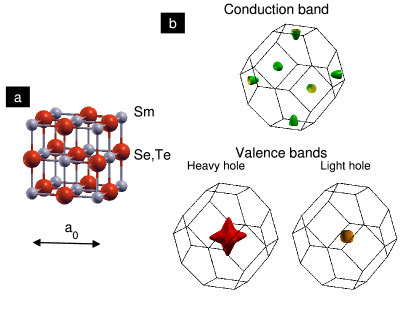
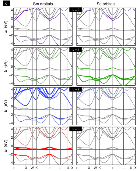
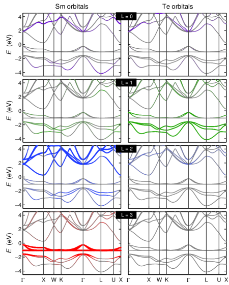
Mixed valence rare-earth compounds SmSe and SmTe have rock-salt crystal structure (Fmm), as depicted in Fig. 1a. Band structure shows them to be indirect band gap semiconductors Antonov et al. (2002); Svane et al. (2004); Gupta and Kulshrestha (2009) with eV. The valence bands maximum is located at the -point and their energy surfaces have octahedral symmetry (as illustrated for the case of SmSe in Fig. 1b). In both systems the valence band is formed by the highly localized Sm-4f states () while the chalcogenide p-bands () reside below the localized Sm-4f band, as shown in Fig. 1c and 2. The conduction band edge, located at the X symmetry point, is mostly formed by the delocalized (mobile) Sm 5d states (). The indirect band gap occurs between the conduction band X point and the valence band point. The direct (optical) band gap is at the X point. The energy surfaces around the X point in the conduction band are well described by ellipsoids (Fig. 1b) and, similarly to silicon, the transverse effective mass is smaller than the longitudinal one ().
| SmSe | SmTe | |||
| Property | Theory | Expt. | Theory | Expt. |
| (Å) | 6.18 | 6.20 Jayaraman et al. (1970a) | 6.578 | 6.595 Chatterjee et al. (1972) |
| (eV) | 0.5 | 0.5 Jayaraman et al. (1970a) | 0.54 | 0.63Jayaraman et al. (1970a) |
| (GPa) | 38.3 | Jayaraman et al. (1974) | 34.0 | Chatterjee et al. (1972) |
| 0.18 | – | 0.18 | – | |
| (GPa) | 93.7 | – | 87.4 | – |
| (GPa) | 10.9 | – | 7.3 | – |
| (GPa) | 24.2 | – | 17.2 | – |
| -0.13 | -Kirk et al. (1972) | -0.13 | -Jayaraman et al. (1970a) | |
Experimental work on these mixed-valence compounds suggests that conduction in these systems is due to electron carriers Batlogg et al. (1976); Matsumura et al. (1997). More recently further experimental work using X-ray-absorption spectroscopy found the thermal promotion of 4f electrons to conducting bands occur at low pressure Jarrige et al. (2013) before hybridization governs the valence transition. Contributions from holes are omitted in spite of the finite bandwidth of the 4f valence band stemming from the mixing between Sm-4f and chalcogenide 5p states (Figs. 1c and 2). We therefore attribute the absence of hole conduction to strong scattering in the Sm 4f band or to an enhancement of the band mass due to strong correlations. The effect of mass enhancement can be inferred from data at low temperatures Maple and Wohlleben (1971); Bader et al. (1973); Varma (1976) where the 4f band width is considerably narrower ( meV) than the first principles calculations, suggesting strong localization of the 4f states in SmX materials (S, Se, Te).
The piezoresistive effect, which is also observed in semiconductors such as silicon or germanium Smith (1954), is particularly large in samarium chalcogenide compounds. The large deformation potential Bardeen and Shockley (1950) rapidly reduces the band gap between the Sm-4f and Sm-5d bands under compressive strain. Consequently electrons are thermally promoted from the localized Sm-4f valence bands to the mobile Sm-5d conduction bands and a continuous (isostructural Svane et al. (2004); Gupta and Kulshrestha (2009); Jarrige et al. (2013)) insulator-to-metal transition arises.
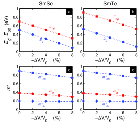
A quantitative description of the piezoresistive effect requires the characterization of changes in the band structure (band gap and effective masses) under strain. Figures 3a and 3b show the indirect (between and X) and direct (at symmetry point X) electronic band gaps as a function of change in volume under isotropic compressive strain in SmSe and SmTe, respectively. The indirect band gap as obtained from first principles is similar for both cases while the optical gap is larger in SmTe than in SmSe. However, they both change at the same rate with strain as observed experimentally Jayaraman et al. (1970a). The carrier effective masses Sze (1981) [] of each band near the Fermi level are also computed: the light hole (lh) and heavy hole (hh) at the point and the electron at the X point. The results show that values are similar for both systems and small reduction with compressive strain (Fig. 3c and 3d).
The piezoresistive gauge is defined as Mason and Thurston (1957):
| (1) |
where is the conductivity and is the field (e.g. strain or pressure). In this work we focus mostly on volumetric strain (i.e. ). Under isotropic strain, pressure and volumetric strain piezoresistive gauges are related by:
| (2) |
where is the bulk modulus. In the diffusive regime, the conductivity can be approximated as modulated by the pressure-dependent charge carrier population in the 5d-conduction band:
| (3) |
where and are the electron density and mobility, respectively. The electron density is expressed as:
| (4) |
where and are the density of states and activation energy (i.e. position of the conduction band relative to the Fermi level), respectively. In Eq. 4 we left implicit the dependence of and on strain.
Neglecting changes with strain in scattering mechanisms the piezoresistive gauge (Eq. 1) can then be approximated by:
| (5) |
From the results obtained from first principles calculations (Fig. 3) we find that the second term on the right hand side of Eq. 5 is more than an order of magnitude smaller than the first one. Therefore the piezoresistive gauge in the Sm monochalcogenide systems is largely governed by the reduction of the activation energy with strain at room temperature or below. Under such conditions, the piezoresistive gauge (Eq. 5) can be estimated using:
| (6) |
We evaluate the piezoresistive response of SmSe and SmTe in two different scenarios using Eq. 4: (i) single crystal under isotropic strain, and (ii) pinned . In the ideal single crystal case under isotropic strain, the Fermi level position can be obtained analytically using the effective masses for each band uni . Using the linear dependence on strain obtained from first principles calculations, we find that the piezoresistive gauge can be approximated as
| (7) |
for these material systems at room temperature.
In reality the presence of defects or impurities levels can place Fermi level away from the middle of the band gap as in ideal crystalline systems. In thin films the Fermi level can also be pinned by the metal contacts when distance between electrodes becomes comparable to the screening length allowing to tailor the piezoresistive gauge in thin films (at larger separations, Fermi-level pinning it is likely controlled strongly by the metal-induced-gap states Tersoff (1984)). For cases where the Fermi-level pinning is unknown, an upper bound value for piezoresistive gauge can be determined:
| (8) |
corresponding to the case where the Fermi level sits at the edge of the valence band. Under isotropic strain, the upper bound at room temperature becomes:
| (9) |
which is very close to the values of 5.3 and 4.9 /GPa for SmSe and SmTe respectively reported by Jayaraman et al Jayaraman et al. (1970a); not . We henceforth conclude that those results under hydrostatic strain are likely near the best possible case scenario within the physics accounted for in our transport model. Because the linear dependence of band gap with strain is a good approximation for large strain (up to %) the piezoresistive gauge remains nearly constant over a large stress/strain range, as observed experimentally.
III Uniaxial strain
In order to analyze the electrical response to stress in SmX thin films Copel et al. (2013) and their potential application in high-performance NEMS such as the piezoelectronic transistor Newns et al. (2012b), the early work on hydrostatic strain must be significantly extended to consider the effects of uniaxial strain. Thus we next quantify the changes in the band structure in SmSe and SmTe for uniaxial strain along the following three directions: [001], [011] and [111], and compare them to the isotropic compression. Note that uniaxial strain transforms the FCC structure (Fmm symmetry) into body centered tetragonal (BCT2), body-centered orthorhombic (ORCI) and rhombohedral (RHL) structures for uniaxial strain along the [001], [011] and [111] directions, respectively. As a consequence of the reduced symmetry degeneracy is lifted and the electronic properties may change differently in different symmetry points (Fig. 4).
In the diffusive regime the piezoresistive response can still be described using Eq. 5. Therefore, differences in the piezoresistive gauge under uniaxial strain can be extracted from the strain dependence of band structure properties in that equation. In particular the sensitivity of the band gap to strain which we have showed earlier to be the most prominent factor.
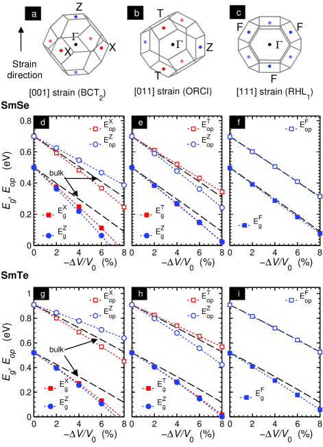
For the uniaxial strain cases considered here the one along the [001]-direction shows the largest change in indirect band gap (), which is about 30% larger than the isotropic case (Fig. 4d and 4g). Note that while pressure (the average of the stress tensor trace) is the same in these two cases, the enhancement emerges at the expense of larger axial component of stress due to the difference between and (Table 1). The reduction in the indirect band gap for strain along the [011] direction is yet larger than that along the [111] direction. In the [111] case, direct and indirect band gaps show similar values to those corresponding to hydrostatic strain. For the cases of uniaxial strain along the [001] and [011] directions the band gaps in different symmetry points exhibit changes at different rates because of the strain-induced symmetry breaking. This effect Smith (1954); Kleinman (1962) is known to not only change the band structure but also impact the mobility and has been exploited in strained Si/Ge interfaces Van de Walle and Martin (1986) and characterized using first principles calculations Fischetti and Laux (1996). However, relative changes in mobility will only be secondary (Eqs. 1 and 5) compared to any change by the band gap.
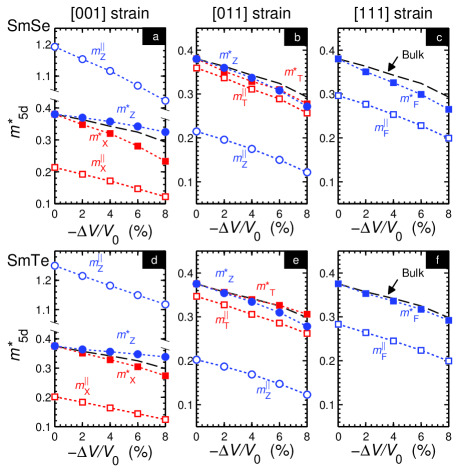
The dependence of the effective mass of the 5d bands (solid symbols in Fig. 5) shows minor differences with the hydrostatic case for both SmSe and SmTe. Therefore it is expected that the piezoresistive gauge under uniaxial strain will still be dominated by the band gap reduction (first term in Eq. 5) and changes of band effective masses playing only a secondary role. In contrast the band mass ban in the direction parallel to the strain direction (open symbols) can be considerably different to the effective mass (solid symbols). For instance the band mass along the [001] direction () can be considerably different to the effective mass () due to the large mass anisotropy. This result has important implications in systems with short channel length as discussed later.
The first demonstration of the piezoresistive effect in thin films Copel et al. (2013) achieved up to nearly half the bulk value in films ranging from 8 up to 50 nm. This less than optimal performance can be attributed to several reasons such as the polycrystalline sample morphology with grain sizes tens of nanometers or the effect of metal electrodes mentioned above. As film quality improves moving toward epitaxial samples a combination of uniaxial strain and proper choice of metal electrodes can be exploited to attain a larger piezoresistive gauge in NEMS applications. Figure 4 suggests that the piezoresistive gauge could be enhanced as much as 30% because of the stronger reduction in band gap with strain.
IV Tunneling
As device sizes shrink, tunneling becomes relevant to conduction. In such scenario crystal orientation exhibits considerably different band masses and thus impacts transport in devices with an ultra short channel. The tunneling current can be estimated following Landauer formalism Di Carlo et al. (1994):
| (10) |
where is the 2-dimensional wave vector in the Brillouin zone perpendicular to the transport direction, and and are the Fermi-Dirac distribution functions on the electrodes.
As a first approximation we can estimate tunneling length in SmX from its CBS neglecting effects of the interface with the electrode. The transmission probability is then taken to be:
| (11) |
where Im() is the imaginary part of the complex wave vector parallel to the strain direction and is the thickness of the SmX films. A more accurate estimate of electrical systems such system requires a complete atomistic description of the metal/SmX interface and is beyond the scope of this work.
Figure 6 shows the CBS of SmSe along the three directions previously considered [001], [011] and [111]. The results are obtained using an empirical tight-binding model accounting for second nearest neighbor coupling with full sets of orbitals Jiang et al. (2013) employing NEMO5 Steiger et al. (2011); Fonseca et al. (2013). The CBS is plotted for the symmetry points where valence and conduction band edges are located.
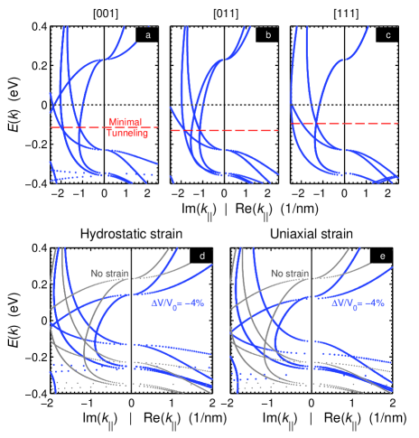
For a fixed energy , a lower bound limit for tunneling (Eq. 11) can be determined using the smallest imaginary part of the complex wave vector at that energy. Overall tunneling in SmX thin films is minimized when the Fermi level position, which may be adjusted using the appropriate metal electrode, is located near the energy where the imaginary wave vectors are the largest. From the CBS presented in Fig. 6, this occurs at an energy level above the valence band edge (as denoted by dashed line). The results indicate that Im() is of the order of 1 nm-1, resulting in a nanometer tunneling length. Thereby the governing conduction mechanism of the bulk (diffusive transport by thermally promoted electrons) is expected to remain dominant as long as the distance between electrodes is larger than the tunneling length. Thus piezoresistive effect is expected to persist in crystalline films with thicknesses of a few nanometers Copel et al. (2013), with metal electrodes playing an important role.
Comparison between the unstrained CBS along different directions shows that the light electron bands may govern tunneling (shortest complex wave vector within the gap) and are approximately similar for all directions. The [001] direction (top row of Fig. 6) shows very different imaginary bands due to the anisotropic mass of the 5d conduction band as previously shown in Fig. 1b. The anisotropy is less significant along the [011] direction and not present for the [111] case.
Study of the changes in the CBS upon the application of isotropic and uniaxial strain shows an overall reduction in the tunneling length. As an example the case of 4% hydrostatic and uniaxial compressive strain are shown in Fig. 6d and 6e, respectively. In all three strain cases, we observe a reduction in the complex wave vector in the band gap and the intersection between imaginary branches where the complex wave vector is the largest still occurs at energies below the middle of the band gap. Similar results were found along the [011] and [111] directions (not plotted here). The uniaxial strain produces a small splitting of the Sm-4f valence bands due to the lifting of degeneracy.
V Conclusions
In summary we have studied the changes in the band structure of SmSe and SmTe under uniaxial strain using first principles calculations and their effect in electronic transport. Our work supports that the large piezoresistive gauge in SmX materials stems from the sensitive deformation potential enabling thermal promotion of carriers from localized valence bands to delocalized conduction bands. The piezoresistive gauge is driven by the change of the electronic band gap with strain as strain dependence of effective masses of valence and conduction bands is more than an order of magnitude smaller. Previous bulk experimental data is reproduced by assuming Fermi level pinning near the valence band edge which gives optimal piezoresistive response. Uniaxial strain can be employed to enhance the piezoresistive properties of Sm monochalcogenide compounds at the price of a larger component of stress along the compression axis (e.g. larger than the corresponding isotropic pressure). For the uniaxial cases studied here, strain applied along the [001] direction exhibits the largest reduction in gap with volume change and thus a piezoresistive gauge larger than that of the isotropic case can be achieved. We find that the sensitivity of SmX thin films can be altered by properly choosing the metal electrodes enabling optimization of the piezoresistive gauge by pinning the Fermi-level near the valence band. Studies of the complex band structure of SmSe show that the tunneling length can be smaller than 1 nm, indicating that the piezoresistive effect driven by thermal promotion of electrons (as observed in the bulk) can be observed in films with thicknesses of a few nanometers.
The authors acknowledge the support from DARPA’s MESO Program under contract N66001-11-C-4109 and an IBM PhD fellowship award. The use of nanoHUB.org computational resources operated by the Network for Computational Nanotechnology funded by the NSF under Grant Nos. EEC-0228390, EEC-1227110, EEC-0228390, EEC-0634750, OCI-0438246, and OCI-0832623 and OCI-0721680 is gratefully acknowledged. NEMO5 developments were critically supported by an NSF Peta-Apps award OCI-0749140 and by Intel Corp. The authors are grateful for fruitful discussion from Yaohua Tan.
References
- Theis and Solomon (2010) T. N. Theis and P. M. Solomon, Science 327, 1600 (2010).
- Newns et al. (2012a) D. Newns, B. Elmegreen, X. H. Liu, and G. Martyna, Journal of Applied Physics 111, 084509 (2012a).
- Barlian et al. (2009) A. Barlian, W.-T. Park, J. Mallon, A. Rastegar, and B. Pruitt, Proceedings of the IEEE 97, 513 (2009).
- Athanassiou et al. (2006) E. K. Athanassiou, R. N. Grass, and W. J. Stark, Nanotechnology 17, 1668 (2006).
- Pang et al. (2012) C. Pang, G.-Y. Lee, T.-i. Kim, S. M. Kim, H. N. Kim, S.-H. Ahn, and K.-Y. Suh, Nature Materials 11, 795 (2012).
- Imada et al. (1998) M. Imada, A. Fujimori, and Y. Tokura, Rev. Mod. Phys. 70, 1039 (1998).
- McWhan et al. (1969) D. B. McWhan, T. M. Rice, and J. P. Remeika, Phys. Rev. Lett. 23, 1384 (1969).
- Marezio et al. (1972) M. Marezio, D. B. McWhan, J. P. Remeika, and P. D. Dernier, Phys. Rev. B 5, 2541 (1972).
- Jayaraman et al. (1970a) A. Jayaraman, V. Narayanamurti, E. Bucher, and R. G. Maines, Phys. Rev. Lett. 25, 1430 (1970a).
- Jayaraman et al. (1970b) A. Jayaraman, V. Narayanamurti, E. Bucher, and R. G. Maines, Phys. Rev. Lett. 25, 368 (1970b).
- Batlogg et al. (1976) B. Batlogg, E. Kaldis, A. Schlegel, and P. Wachter, Phys. Rev. B 14, 5503 (1976).
- Matsumura et al. (1997) T. Matsumura, T. Kosaka, J. Tang, T. Matsumoto, H. Takahashi, N. Môri, and T. Suzuki, Phys. Rev. Lett. 78, 1138 (1997).
- Cavalleri et al. (2004) A. Cavalleri, T. Dekorsy, H. H. W. Chong, J. C. Kieffer, and R. W. Schoenlein, Phys. Rev. B 70, 161102 (2004).
- Luo et al. (2004) Q. Luo, Q. Guo, and E. G. Wang, Applied Physics Letters 84, 2337 (2004).
- Copel et al. (2013) M. Copel, M. A. Kuroda, M. S. Gordon, X.-H. Liu, S. S. Mahajan, G. J. Martyna, N. Moumen, C. Armstrong, S. M. Rossnagel, T. M. Shaw, P. M. Solomon, T. N. Theis, J. J. Yurkas, Y. Zhu, and D. M. Newns, Nano Letters 13, 4650 (2013).
- Farberovich (1980) O. V. Farberovich, Sov. Phys. Solid State 22, 393 (1980).
- Antonov et al. (2002) V. N. Antonov, B. N. Harmon, and A. N. Yaresko, Phys. Rev. B 66, 165208 (2002).
- Svane et al. (2004) A. Svane, G. Santi, Z. Szotek, W. M. Temmerman, P. Strange, M. Horne, G. Vaitheeswaran, V. Kanchana, L. Petit, and H. Winter, physica status solidi (b) 241, 3185 (2004).
- Gupta and Kulshrestha (2009) D. C. Gupta and S. Kulshrestha, Journal of Physics: Condensed Matter 21, 436011 (2009).
- Petit et al. (2014) L. Petit, A. Svane, M. Lüders, Z. Szotek, G. Vaitheeswaran, V. Kanchana, and W. M. Temmerman, Journal of Physics: Condensed Matter 26, 274213 (2014).
- Newns et al. (2012b) D. M. Newns, B. G. Elmegreen, X.-H. Liu, and G. J. Martyna, Advanced Materials 24, 3672 (2012b).
- Langreth and Perdew (1980) D. C. Langreth and J. P. Perdew, Phys. Rev. B 21, 5469 (1980).
- Perdew et al. (1996) J. P. Perdew, K. Burke, and M. Ernzerhof, Phys. Rev. Lett. 77, 3865 (1996).
- (24) http://elk.sourceforge.net/ .
- (25) This choice impacts the result of the equilibrium lattice constant and the size of the electronic band gap which is not always properly estimated in DFT [C. S. Wang and W. E. Pickett, Phys. Rev. Lett. 51, 597 (1983)]. However, the change of band gap with pressure is less sensitive to this choice.
- Chatterjee et al. (1972) A. Chatterjee, A. K. Singh, and A. Jayaraman, Phys. Rev. B 6, 2285 (1972).
- Jayaraman et al. (1974) A. Jayaraman, A. K. Singh, A. Chatterjee, and S. U. Devi, Phys. Rev. B 9, 2513 (1974).
- Kirk et al. (1972) J. L. Kirk, K. Vedam, V. Narayanamurti, A. Jayaraman, and E. Bucher, Phys. Rev. B 6, 3023 (1972).
- Jarrige et al. (2013) I. Jarrige, H. Yamaoka, J.-P. Rueff, J.-F. Lin, M. Taguchi, N. Hiraoka, H. Ishii, K. D. Tsuei, K. Imura, T. Matsumura, A. Ochiai, H. S. Suzuki, and A. Kotani, Phys. Rev. B 87, 115107 (2013).
- Maple and Wohlleben (1971) M. B. Maple and D. Wohlleben, Phys. Rev. Lett. 27, 511 (1971).
- Bader et al. (1973) S. D. Bader, N. E. Phillips, and D. B. McWhan, Phys. Rev. B 7, 4686 (1973).
- Varma (1976) C. M. Varma, Rev. Mod. Phys. 48, 219 (1976).
- Smith (1954) C. S. Smith, Phys. Rev. 94, 42 (1954).
- Bardeen and Shockley (1950) J. Bardeen and W. Shockley, Phys. Rev. 80, 72 (1950).
- Sze (1981) S. Sze, Physics of Semiconductor Devices, Wiley-Interscience publication (John Wiley & Sons, 1981).
- Mason and Thurston (1957) W. P. Mason and R. N. Thurston, The Journal of the Acoustical Society of America 29, 1096 (1957).
- (37) If strain is not isotropic the top of the two valence bands split and problem cannot be solved analytically.
- Tersoff (1984) J. Tersoff, Phys. Rev. Lett. 52, 465 (1984).
- (39) The experimentally measured piezoresistive gauge in SmTe shows a kink at low pressures which the authors have been attributed to trap levels [9].
- Kleinman (1962) L. Kleinman, Phys. Rev. 128, 2614 (1962).
- Van de Walle and Martin (1986) C. G. Van de Walle and R. M. Martin, Phys. Rev. B 34, 5621 (1986).
- Fischetti and Laux (1996) M. V. Fischetti and S. E. Laux, Journal of Applied Physics 80, 2234 (1996).
- (43) The band mass is computed employing the curvature of the electronic bands as obtained from first-principles.
- Di Carlo et al. (1994) A. Di Carlo, P. Vogl, and W. Pötz, Phys. Rev. B 50, 8358 (1994).
- Jiang et al. (2013) Z. Jiang, M. A. Kuroda, Y. Tan, D. M. Newns, M. Povolotskyi, T. B. Boykin, T. Kubis, G. Klimeck, and G. J. Martyna, Applied Physics Letters 102, 193501 (2013).
- Steiger et al. (2011) S. Steiger, M. Povolotskyi, H.-H. Park, T. Kubis, and G. Klimeck, Nanotechnology, IEEE Transactions on 10, 1464 (2011).
- Fonseca et al. (2013) J. Fonseca, T. Kubis, M. Povolotskyi, B. Novakovic, A. Ajoy, G. Hegde, H. Ilatikhameneh, Z. Jiang, P. Sengupta, Y. Tan, and G. Klimeck, Journal of Computational Electronics 12, 592 (2013).