Light-Matter Interaction and Lasing in Semiconductor Nanowires:
A combined FDTD and Semiconductor Bloch Equation Approach
Abstract
We present a time-domain model for the simulation of light-matter interaction in semiconductors in arbitrary geometries and across a wide range of excitation conditions. The electromagnetic field is treated classically using the finite-difference time-domain method. The polarization and occupation numbers of the semiconductor material are described using the semiconductor Bloch equations including many-body effects in the screened Hartree-Fock approximation. Spontaneous emission noise is introduced using stochastic driving terms. As an application, we present simulations of the dynamics of a nanowire laser including optical pumping, seeding by spontaneous emission and the selection of lasing modes.
pacs:
42.55.Px, 71.35.Cc, 74.25.GzI Introduction
Semiconductor lasers are important components of optical technologies with numerous applications in daily life. Their large scale use, e.g. in optical networks, has raised the need for reduced power consumption as a contribution to global energy savings. Therefore, semiconductor nanolasers are at the forefront of current research to meet this need. Recently, semiconductor nanowires have attracted widespread interest due to their unique combination of electrical and optical properties, which allow for applications as photonic and plasmonic lasers or as resonators for the observation of polaritonic effects.Duan et al. (2003); Oulton et al. (2009); Sidiropoulos et al. (2014); Saxena et al. (2013); Roeder et al. (2013) Many applications rely on sophisticated geometries, where bending and folding of individual wires or the interaction between multiple wires play an important role in determining the optical properties.Xiao et al. (2011); Xu et al. (2012)
On the other hand, the performance of a nanolaser device relies heavily on the electronic properties of the respective gain material. In nanowire laser systems, the gain is typically provided by the wire material itself. Alternatively additional constituents such as incorporated transition metal or rare-earth ions can provide the gain. For semiconductor active materials, the single-particle electronic states are defined by structural properties such as material composition, quantum confinement and strain.
The optical properties, however, are additionally influenced by many-body effects of the excited carriers. In the weakly excited regime, these effects give rise to excitonic absorption peaks lying below the band gap. In the high excitation regime, the excitation dependence of the optical gain is dominated by phase-space filling and many-body energy renormalizations. Coulomb enhancement of interband transitions, screening, and excitation induced dephasing additionally contribute to magnitude and spectral distribution of the gain ElSayed et al. (1994); Chow and Koch (1999); Haug and Koch (2004); Manzke and Henneberger (2002). Therefore, a predictive theory of nanowire lasing needs to incorporate these effects as well as the device geometry.
Numerical methods like finite-difference time-domainTaflove and Hagness (2005) (FDTD) simulations allow for the modelling of electrodynamics in arbitrarily complex geometries and can be readily extended to solve additional differential equations describing dispersive, nonlinear or gain media. However, while this approach has been used to model semiconductor media using incoherently coupled two-level systems Huang and Ho (2006), the combination of the FDTD method with a proper semiconductor gain model, including excitonic and band-gap renormalization effects is still lacking. To bridge this gap, we present a theoretical model combining semiconductor Bloch equationsHaug and Koch (2004) with the FDTD method. The Coulomb interaction is treated in the screened Hartree-Fock approximationChow and Koch (1999) to provide for an accurate description across different excitation density regimes. Since nanowire lasing modes usually have a non-trivial polarization structure, several bands and electronic transitions need to be included in order to describe the coupling of different electric field polarizations to the material.
As a first application, we present simulations of the dynamics of an optically pumped semiconductor nanowire, including the amplification of spontaneous emission up to the onset of lasing and the selection of transverse and longitudinal modes.
II Theoretical Model
II.1 General formulation
To investigate light-matter interaction in semiconductor NWs, we solve Maxwells equations
| (1) |
| (2) |
| (3) |
using the standard FDTD algorithm Yee (1966); Taflove and Hagness (2005) and taking into account the full vectorial character of the electric field , the magnetic induction and the dielectric displacement . The passive material response is incorporated in a nondispersive dielectric constant , while the dynamic action of the semiconductor material is represented by the polarization , which includes contributions from all optical transitions from valence bands with indices to the conduction band (index ) at electron Bloch vectors . We assume the microscopic polarizations as well as the occupation numbers for conduction-band electrons () and for holes in the different valence bands () to depend only on the absolute value of the Bloch vector, so that the polarization in a bulk semiconductor takes the form
| (4) |
where is the dipole matrix element attributed to the transition from valence band to the conduction band and coupling to the electric field component pointing in direction . To explicitly take into account the nature of the active material, we employ semiconductor Bloch equations (SBE) Haug and Koch (2004) in the screened exchange-Coulomb hole approximation Chow and Koch (1999).
This leads to equations of motion for the microscopic interband polarisations of the form
| (5) |
with the renormalized Rabi frequency
| (6) |
using the screened Coulomb matrix elements . We include an excitation density dependent dephasing caused by carrier-carrier Coulomb interaction Haug (2000). Transition energies are defined by the band gap energy and the renormalized single-particle energies
| (7) |
where are the effective masses. The Coulomb hole contribution can be written as
| (8) |
where is the unscreened Coulomb matrix element Binder and Koch (1995). The screened and unscreened Coulomb interaction is given by
| (9) |
with screening wavenumber
| (10) |
and by
| (11) |
respectively. To evaluate these matrix elements numerically, we utilize an angle-averaging procedure, which is described in Haug and Koch (2004). This yields the matrix elements and that are used above.
Similar to the equation of motion for the transition amplitudes, the time evolution of the occupation numbers is given by
| (12) |
for electrons and by
| (13) |
for holes in the valence band . The first term describes the carrier excitation by the electromagnetic field. The two terms involving and respectively phenomenologically describe non-radiative recombination and intra-band relaxation of carriers towards Fermi-Dirac distributions with a band dependent fermi level. Huang and Ho (2006). To allow for the relaxation between valence bands, an additional contribution is included in the equation of motion for the hole populations, where
| (14) |
To allow for the description of spontaneous emission in our semiclassical model, we add noise terms as previously used for two-level systemsAndreasen and Cao (2010, 2009)
| (15) |
to the right hand side of equation 5 as well as
| (16) |
| (17) |
to the right hand sides of equations 12 and 13. are gaussian random numbers with zero mean. The individual are coupled by the Coulomb interaction, therefore excitonic effects are included in the spontaneous emission, which lies mainly below the band gap. The intra-band relaxation processes associated with and are microscopically caused by a combination of carrier-carrier Coulomb scattering and carrier-phonon scattering and redistribute the populations towards quasi-Fermi distributions. These processes do not describe a decay of polarization and conserve quasi-particle densities. Therefore associated additional noise amplitudes can be safely neglected, at least for high excitation densities and in the lasing regime.
II.2 Optical transitions for 2-6 Semiconductors
Simulations of photonic nanostructures require a fully vectorial treatment including the coupling of all electric field components to the material system. Therefore the consideration of all transition elements between bands in a relevant frequency range is necessary. In this section we discuss the involved bands and the possible transitions for the case of 2-6 semiconductors with wurtzite structure (Fig. 1). These materials are most interesting in the case of nanowire lasers. However our algorithm can be easily modified to simulate other band structures.
Photonic wires with wurtzite structure are birefringent with the optical axes pointing in -direction along the wire. The optical properties arise from transitions between three p-like valence bands (occupation numbers , ) and a single s-like conduction band (occupation number ).Thomas and Hopfield (1959, 1962)

The degeneracy of the valence bands (total angular momentum , -component ), () and (, ) is lifted due to spin-orbit coupling and interaction with the hexagonal crystal field. Valence band can be safely neglected in a description of the optical properties, since its energy is significantly set off from the fundamental band gap. Thus, the relevant occupation numbers for our model are .
To find all possible transitions and their respective relative dipole matrix elements, states are expanded in spin- and orbital angular momentum eigenstates using Clebsch-Gordan coefficients. Assuming conservation of electron spin, allowed optical transitions are characterized by a conservation of angular momenta of photons and electrons. Light polarized linearly along the -axis aligned with the crystals -axis induces transitions with . A transition with corresponds to circular polarization in the -plane perpendicular to the -axis. These transitions are expanded in a linear polarization basis to allow for coupling to FDTD simulations.
We obtain two possible transitions between valence band and the conduction band coupling to - and -polarized light with dipole matrix elements . Valence band turns out to be active for all three polarization directions and we obtain dipole matrix elements and .
II.3 Parameters for CdS
In this work we focus on CdS nanowire structures. Gap energies for the two relevant bands and are taken from theoretical calculations.Ekuma et al. (2011); Zakharov et al. (1994) Anisotropic effective masses found in literaturecds (1999) have to be angle-averaged to be applied in our model, where only the absolute values of the -vector are used. We obtain for electrons as well as and for holes. The background refractive index has been chosen so that reported values for the exciton binding energyGutowski et al. (2009) are reproduced. The dipole matrix element is taken from literature.Hassan (1993)
We use a density-dependent dephasing time-constant similiar to experimental and theoretical literatureHügel et al. (2000); Haug (2000)
| (18) |
III Results
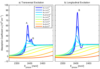
In order to probe the linear response of our material model, we simulate a thin CdS sample in air irradiated with a plane wave and record the spectrum of the electric field and the polarization inside the sample. From this, the electronic contribution to the permittivity is calculated and the absorption coefficient is obtained. For an excitation polarized perpendicularly to the crystals -axis (), the absorption spectrum shows two distinct peaks corresponding to the exciton 1s resonances of the transitions between each of the valence bands and the conduction band (Fig. 2(a)). For an excitation along the -axis (), only one absorption peak can be observed, since for this polarization only the transition from valence band to the conduction band is accessible (Fig. 2(b)). In both cases the exciton peaks vanish for higher excitation densities due to the combined effects of screening and band filling.
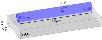
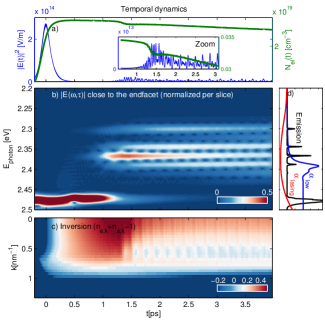
We now turn our attention to the lasing dynamics of optically excited nanowire lasers. We simulate a nanowire with diameter and length extending along the -axis centered on and resting on a fused silica substrate as shown in Fig. 3. The wire is pumped from above (-direction) with a -polarized plane wave pump pulse with a sech-shaped time dependence (central wavelength , temporal width ). To inject this excitation pulse, we utilize the total field / scattered field (TF/SF) formalism,Taflove and Hagness (2005) which allows for the excitation of a plane wave inside a bounded simulation volume. Outside the TF/SF border, only fields scattered or emitted by the nanowire are present. Fig. 4(a) shows the temporal dynamics of the electric field and of the electron density. The electron density is recorded in a slice perpendicular to the wire axis positioned close to an endfacet (). The electric field intensity is averaged across a slice outside the wire (). After applying a windowed Fourier transform to the time-domain data, the dynamics of the involved modes can be studied (Fig. 4(b)).
Starting from thermal equilibrium, the conduction band electron density is pumped by the excitation pulse, which is centered at . After the passage of the excitation pulse, intensities drop until stimulated emission sets in with a steep rise at about (Inset of Fig. 4(a)). The presence of equally spaced modes in the time-dependent spectra (Fig. 4(b)) indicates lasing emission from approximately up to the end of the simulation window. Initially, the emission is dominated by a single longitudinal mode, which is rapidly amplified and depletes the material gain, until the emission reaches its maximum value at . At this point, power is redistributed to other longitudinal modes which can access the remaining material gain. The lasing emission continues with a slowly falling slope, leading to a strongly asymmetric shape of the emitted pulse sequence. Due to interference between the lasing modes the emitted pulse sequence has a rather irregular temporal shape.
The -resolved inversion of the transition from valence band to the conduction band is plotted in Fig. 4(c). The pump pulse is positioned at higher energies than the plotted Bloch vector states. The lasing pulse initially depletes excitations in a region of wavevector space around . This explains, why modes which mostly access other regions of -space are still weakly amplified and continue to lase after the maximum of the overall emission.
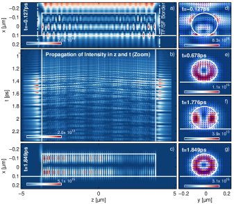
Fig. 5(b) shows the spatiotemporal dynamics of the lasing process. The electric field intensity averaged over each -slice is plotted over time and over the length of the simulation volume along the -direction. Initially, the field maxima inside the wire keep a fixed location along the -axis, as expected for nearly single-mode lasing action. As the initial emission peak is reached, the field profile along the wire gets strongly modulated, since the contribution of additional longitudinal modes becomes relevant.
Apart from longitudinal modes, the properties of a nanowire laser are also strongly influenced by transverse modes. The transverse field structure determines the modal gain as well as the mode reflectivity at the end facets of the nanowire.Maslov and Ning (2003); Maslov and Ning (2004) Figs. 5(d-g) show the transverse fields across a slice () of the nanowire at different times during the simulation. Figs. 5(a,d) display the scattering of the incident pump light on the nanowire, leading to a spatially inhomogeneous pump profile. In Figs. 5(e-g), the mode dynamics after the onset of lasing can be observed. As predicted from linear calculations,Roeder et al. (2014) the field profiles of wires of the investigated diameter range are dominated by the HE21 mode, which has a high modal reflectivity as well as a high confinement factor. However, the field profile is fluctuating between the individual timesteps, indicating an admixture of additional transverse modes. This is especially visible in panel (f), where the polarization of the HE21 mode is still recognizable, but the intensity profile differs significantly from that of the pure mode. Panels (e) and (g) show almost pure HE21 mode profiles.
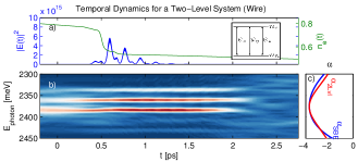
As the numerical treatment of semiconductor Bloch equations is quite cumbersome one might be tempted to restrict to simpler material models. Indeed some of the observed dynamical features are not inherent to the semiconductor material, but more to the wire geometry. However others require the material model to be reproduced. For comparison, we include a simulation of a nanowire laser where the active material is described by a two-level system, as often employed in FDTD simulations. The transition between the two levels couples equally to all three field polarizations (see Inset of Fig.6(a) ). The material is assumed to be excited to an upper-level occupation of and material parameters are tuned to fit the gain profile of highly excited CdS. We observe, that even though the gain profile (Fig. 6(c)) looks very similiar to that of the semiconductor material, the resulting lasing dynamics differ considerably. As opposed to the full model, there is no prolonged stimulated emission after the initial peak, leading to a more symmetric temporal shape of the emission. (Fig. 6(a)). Since the shape of the gain profile of a single two-level system does not change as carriers are depleted, the spectral shape of the emission stays approximately constant during lasing action (Fig. 6(b)). Lasing emission stops as soon as the dominant mode no longer fulfills the lasing condition.
IV Conclusions
We presented a theoretical model for the simulation of light-matter interaction in arbitrarily shaped semiconductor structures based on the FDTD method and the semiconductor Bloch equations. We adapted the model to the band structure of 2-6 semiconductors and presented simulations of the lasing dynamics of an optically pumped CdS-nanowire. Our model allows for the description of semiconductors across the whole range of excitation conditions from the weakly excited case to the lasing regime and is not limited to equilibrium distributions of carriers either in Bloch vector or real space. Thus it is especially interesting for lasing simulations where excitation conditions vary strongly across space or time as well as for simulations of nonlinear optical phenomena in the weakly to moderately excited regime.
Acknowledgements.
The authors gratefully acknowledge financial support by Deutsche Forschungsgemeinschaft (Forschergruppe FOR1616, projects P5 and E4). Robert Buschlinger acknowledges financial support from the International Max Planck Research School Physics of Light.References
- Duan et al. (2003) X. Duan, Y. Huang, R. Agarwal, and C. M. Lieber, Nature 421, 241 (2003), URL http://dx.doi.org/10.1038/nature01353.
- Oulton et al. (2009) R. F. Oulton, V. J. Sorger, T. Zentgraf, R.-M. Ma, C. Gladden, L. Dai, G. Bartal, and X. Zhang, Nature 461, 629 (2009), URL http://dx.doi.org/10.1038/nature08364.
- Sidiropoulos et al. (2014) T. P. H. Sidiropoulos, R. Roder, S. Geburt, O. Hess, S. A. Maier, C. Ronning, and R. F. Oulton, Nat Phys advance online publication (2014), ISSN 1745-2481, URL http://dx.doi.org/10.1038/nphys310310.1038/nphys3103http://www.nature.com/nphys/journal/vaop/ncurrent/abs/nphys3103.html#supplementary-information.
- Saxena et al. (2013) D. Saxena, S. Mokkapati, P. Parkinson, N. Jiang, Q. Gao, H. H. Tan, and C. Jagadish, Nature Photonics 7, 963 (2013), URL http://dx.doi.org/10.1038/nphoton.2013.303.
- Roeder et al. (2013) R. Roeder, M. Wille, S. Geburt, J. Rensberg, M. Zhang, J. G. Lu, F. Capasso, R. Buschlinger, U. Peschel, and C. Ronning, Nano Letters 13, 3602 (2013), eprint http://pubs.acs.org/doi/pdf/10.1021/nl401355b, URL http://pubs.acs.org/doi/abs/10.1021/nl401355b.
- Xiao et al. (2011) Y. Xiao, C. Meng, P. Wang, Y. Ye, H. Yu, S. Wang, F. Gu, L. Dai, and L. Tong, Nano Letters 11, 1122 (2011), eprint http://pubs.acs.org/doi/pdf/10.1021/nl1040308, URL http://pubs.acs.org/doi/abs/10.1021/nl1040308.
- Xu et al. (2012) H. Xu, J. B. Wright, T.-S. Luk, J. J. Figiel, K. Cross, L. Lester, G. Balakrishnan, G. T. Wang, I. Brener, and Q. Li, Applied Physics Letters 101, 113106 (2012), ISSN 0003-6951.
- ElSayed et al. (1994) K. ElSayed, L. Bányai, and H. Haug, Phys. Rev. B 50, 1541 (1994).
- Chow and Koch (1999) W. Chow and S. Koch, Semiconductor-Laser Fundamentals (Springer-Verlag, Berlin, 1999), 1st ed.
- Haug and Koch (2004) H. Haug and S. Koch, Quantum Theory of the Optical and Electronic Properties of Semiconductors (4th Edition) (World Scientific, 2004), ISBN 9789812387561, URL http://books.google.de/books?id=-UoG0Hx0w04C.
- Manzke and Henneberger (2002) G. Manzke and K. Henneberger, phys. stat. sol. (b) 234, 233 (2002).
- Taflove and Hagness (2005) A. Taflove and S. C. Hagness, Computational Electrodynamics: The Finite-Difference Time-Domain Method (Artech House, 2005).
- Huang and Ho (2006) Y. Huang and S.-T. Ho, Opt. Express 14, 3569 (2006), URL http://www.opticsexpress.org/abstract.cfm?URI=oe-14-8-3569.
- Yee (1966) K. S. Yee, IEEE Transactions on Antennas and Propagation AP-14, 302 (1966).
- Haug (2000) H. Haug, physica status solidi (b) 221, 179 (2000), ISSN 1521-3951, URL http://dx.doi.org/10.1002/1521-3951(200009)221:1<179::AID-PSSB179>3.0.CO;2-6.
- Binder and Koch (1995) R. Binder and S. Koch, Progress in Quantum Electronics 19, 307 (1995), ISSN 0079-6727, URL http://www.sciencedirect.com/science/article/pii/007967279500001S.
- Andreasen and Cao (2010) J. Andreasen and H. Cao, Phys. Rev. A 82, 063835 (2010), URL http://link.aps.org/doi/10.1103/PhysRevA.82.063835.
- Andreasen and Cao (2009) J. Andreasen and H. Cao, J. Lightwave Technol. 27, 4530 (2009), URL http://jlt.osa.org/abstract.cfm?URI=jlt-27-20-4530.
- Thomas and Hopfield (1959) D. G. Thomas and J. J. Hopfield, Phys. Rev. 116, 573 (1959), URL http://link.aps.org/doi/10.1103/PhysRev.116.573.
- Thomas and Hopfield (1962) D. G. Thomas and J. J. Hopfield, Phys. Rev. 128, 2135 (1962), URL http://link.aps.org/doi/10.1103/PhysRev.128.2135.
- Ekuma et al. (2011) E. C. Ekuma, L. Franklin, G. L. Zhao, J. T. Wang, and D. Bagayoko, Canadian Journal of Physics 89, 319 (2011), eprint http://www.nrcresearchpress.com/doi/pdf/10.1139/P11-023, URL http://www.nrcresearchpress.com/doi/abs/10.1139/P11-023.
- Zakharov et al. (1994) O. Zakharov, A. Rubio, X. Blase, M. L. Cohen, and S. G. Louie, Phys. Rev. B 50, 10780 (1994), URL http://link.aps.org/doi/10.1103/PhysRevB.50.10780.
- cds (1999) in II-VI and I-VII Compounds; Semimagnetic Compounds, edited by O. Madelung, U. Rössler, and M. Schulz (Springer Berlin Heidelberg, 1999), vol. 41B of Landolt-Börnstein - Group III Condensed Matter, pp. 1–4, ISBN 978-3-540-64964-9, URL http://dx.doi.org/10.1007/10681719_527.
- Gutowski et al. (2009) J. Gutowski, K. Sebald, and T. Voss, in Semiconductors, edited by U. Roessler (Springer Berlin Heidelberg, 2009), vol. 44B of Landolt-Bï¿œrnstein - Group III Condensed Matter, pp. 40–43, ISBN 978-3-540-74391-0, URL http://dx.doi.org/10.1007/978-3-540-74392-7_27.
- Hassan (1993) A. Hassan, Optics Communications 98, 80 (1993), ISSN 0030-4018, URL http://www.sciencedirect.com/science/article/pii/003040189390762T.
- Hügel et al. (2000) W. Hügel, M. Heinrich, and M. Wegener, physica status solidi (b) 473, 473 (2000), URL http://onlinelibrary.wiley.com/doi/10.1002/1521-3951(200009)221:1%3C473::AID-PSSB473%3E3.0.CO;2-I/abstract.
- Qi et al. (1988) J. Qi, K. Shi, G. Xiong, and X. Xu, Journal of Luminescence 40-41, 575 (1988), ISSN 0022-2313, URL http://www.sciencedirect.com/science/article/pii/0022231388903377.
- Maslov and Ning (2003) A. V. Maslov and C. Z. Ning, Applied Physics Letters 83, 1237 (2003), URL http://scitation.aip.org/content/aip/journal/apl/83/6/10.1063/1.1599037.
- Maslov and Ning (2004) A. Maslov and C.-Z. Ning, Quantum Electronics, IEEE Journal of 40, 1389 (2004), ISSN 0018-9197.
- Roeder et al. (2014) R. Roeder, D. Ploss, A. Kriesch, R. Buschlinger, S. Geburt, U. Peschel, and C. Ronning, Journal of Physics D 47, 394012 (2014), URL http://dx.doi.org/10.1088/0022-3727/47/39/394012http://arxiv.org/abs/1407.6744.