Non-linear spin transport in a rectifying ferromagnet/semiconductor Schottky contact
Abstract
The electrical creation and detection of spin accumulation in ferromagnet/semiconductor Schottky contacts that exhibit highly non-linear and rectifying electrical transport is evaluated. If the spin accumulation in the semiconductor is small, the expression for the spin voltage is identical to that of linear transport. However, if the spin accumulation is comparable to the characteristic energy scale that governs the degree of non-linearity, the spin detection sensitivity and the spin voltage are notably reduced. Moreover, the non-linearity enhances the back-flow of spins into the ferromagnet and its detrimental effect on the injected spin current, and the contact resistance required to avoid back-flow is larger than for linear transport. It is also shown that by virtue of the non-linearity, a non-magnetic metal contact can be used to electrically detect spin accumulation in a semiconductor.
I Introduction
The development of electronic devices and circuits that use spin to encode digital
information is an attractive alternative to charge-based computing,
particularly if the unique attributes of semiconductors (amplification) and ferromagnets
(non-volatility) can be combined into a unified and energy-efficient computing technology.
Much progress has recently been made in developing the basic building blocks of such a
semiconductor spintronics technology chappert ; awschalom ; fertnobel ; jansennmatreview ; jansensstreview .
Since mainstream semiconductors such as silicon
and GaAs are non-magnetic and in equilibrium do not possess any spin polarization, contacts
between a ferromagnet (FM) and a semiconductor (SC) are key components. On the one hand,
such junctions enable the transfer of spins from the ferromagnetic reservoir into the
semiconductor and thereby the creation of a sizeable (non-equilibrium) spin polarization of the
carriers in the semiconductor. Equally important, a ferromagnetic contact can
probe the spin polarization in a semiconductor and convert it into a detectable signal.
In order to efficiently inject spins from a ferromagnetic metal into a semiconductor,
an interfacial energy barrier with a sufficiently large resistance times area (RA) product is
needed. This interface barrier limits the back-flow of the accumulated spins from the semiconductor
into the ferromagnetic source and avoids the so-called conductivity mismatch that prevents
spin injection from contacts with vanishingly small RA product jansensstreview ; schmidt .
Therefore, ferromagnetic contacts on semiconductors are either FM/I/SC structures, where
I is a thin tunnel insulator, or direct FM/SC contacts in which the Schottky barrier
formed at the metal/SC interface provides the energy barrier. In the latter case one
normally employs a semiconductor with a heavily-doped surface region or a -doping
layer near the surface in order to obtain a Schottky barrier with a narrow depletion region
and an appropriate RA-product.
Hitherto, it has been common practise to compare the experimental spin signals for
such structures to the theory previously developed for spin injection from a ferromagnetic
metal into a non-magnetic metal fertprb ; fertieee ; jaffres ; maekawa ; dery , which starts
from a linear current-voltage relation. While this is appropriate for metallic junctions,
it does not capture the features that are specific for semiconductor junctions. These include
the energy band profile in the semiconductor and the associated energy barrier (Schottky
barrier), the localized states formed at the I/SC interface, as well as non-linear,
rectifying and/or thermally-activated transport. To better describe the experimental
results for magnetic tunnel devices on semiconductors, some of these aspects have
been examined derysham ; jansenprl ; tran ; jansentwostep ; derymr ; tanamoto ; selberherr .
Notably, for FM/SC Schottky contacts it was described derysham how spin transport is
changed due to the subsurface potential well that is formed in the semiconductor due to the
doping profile (heavily-doped surface layer on a substrate with lower doping density).
For FM/I/SC junctions, the presence of two barriers (tunnel insulator and Schottky barrier)
was shown to alter the spin detection efficiency when transport across the Schottky barrier
is by thermionic emission jansenprl . Subsequently, spin injection by two-step tunneling via
interface states near the semiconductor surface was modeled and it was elucidated that this
transport process can modify spin signals in a profound way tran . Important additions to
and refinements of the latter model have also been reported jansentwostep ; derymr ; note1 .
Here we evaluate spin transport in a direct Schottky contact between a ferromagnetic
metal and a semiconductor with a homogeneous doping density. We consider electrical transport
across the interface that is highly non-linear (i.e., rectifying, diode-like) and present
a theory to describe the electrical creation of a spin accumulation and its electrical
detection via the Hanle effect. It is shown, by explicit evaluation starting from
spin-dependent non-linear transport equations, that for a rectifying Schottky
diode the expressions for the spin current, spin-detection sensitivity and the detectable
spin voltage signal are essentially the same as those of linear models, provided that the
spin splitting in the SC is small compared to the energy scale that governs
the degree of non-linearity of the transport across the interface. When is larger
and comparable to , the non-linearity causes a reduction in the spin detection sensitivity
of the contact as well as a significant enhancement of the back-flow of spins into the
ferromagnetic electrode as compared to linear transport. Importantly, the non-linearity does not
produce any enhancement of the detectable spin signal. We discuss our results in light of
previous descriptions of the effect of the contact non-linearity on the spin
signals pu ; shiogai ; appelbaumdidv in which the essential ratio of and
does not appear. Finally, it is shown that the non-linearity enables a novel means to electrically
detect an (externally generated) spin accumulation in a semiconductor, namely by using
a rectifying contact with a non-magnetic metal electrode.
II Summary of linear spin transport theory
Let us first briefly summarize the results of the theory previously developed for spin injection from a ferromagnetic metal into a non-magnetic metal, which starts from a linear current-voltage relation fertprb ; fertieee ; jaffres ; maekawa ; dery . The voltage across such a contact is the sum of the regular resistive contribution (, with the current density and the RA-product of the contact in the absence of spin accumulation) and an additional contribution, the spin voltage, given by . Here is the conductance spin polarization of the contact and is the induced spin accumulation, represented by a spin splitting between the electrochemical potentials and of the electrons with spin pointing up or down, respectively. The magnitude of is proportional to the density of injected spin current and to the so-called spin resistance of the non-magnetic material (i.e., ). Experimentally, the spin voltage can be detected jansennmatreview via a measurement of the Hanle effect, in which the spin accumulation is reduced to zero by spin precession in an external transverse magnetic field. Keeping the current constant, this results in a change in the voltage across the contact equal to the spin voltage.
III Theory of spin transport in a rectifying contact
The model we introduce to describe non-linear spin transport starts from the expressions for electronic transport across a direct metal-semiconductor contact by thermionic emission sze . The basic parameters are the bias voltage , the temperature and the height of the Schottky barrier. Including the spin splitting of the electrochemical potential in the semiconductor, the currents of majority and minority spin electrons, and , respectively, are:
| (1) | |||
| (2) |
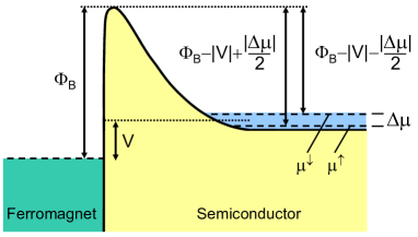
Here, is the electronic charge and the voltage is defined as , with the potential of the ferromagnetic electrode and the spin-averaged potential of the semiconductor. The forward bias condition (see Fig. 1) of the contact thus corresponds to negative voltage and current density. The spin-dependent conductance of a Schottky contact with a ferromagnetic metal is included via the pre-factors:
| (3) | |||
| (4) |
The is the modified Richardson’s constant sze that incorporates the finite probability of
reflection at the semiconductor-ferromagnet interface, which also produces the non-zero spin
polarization of the conductance
across the contact. The parameter is a characteristic energy scale that controls the degree of non-linearity.
For pure thermionic emission , with the Boltzmann constant. When there is also a contribution from
tunneling through the Schottky barrier the expressions have the same form, but the pre-factor is different and
the energy scale is changed to , where is the so-called ideality factor sze . Since
this reduces the non-linearity.
At small enough bias () the transport approaches the linear regime without
rectification. Since spin transport in the linear regime has been described previously, we
shall focus here on the non-linear regime and consider a sufficiently large forward bias
such that . The total charge current and
the spin current across the contact are then:
| (5) | |||
| (6) |
The way the spin accumulation is incorporated into the expressions for thermionic emission deserves some attention. First, it is noted that the presence of the spin accumulation in the semiconductor does not affect the current due to thermal emission of electrons over the Schottky barrier in the direction from the ferromagnet to the semiconductor. The emission barrier height is given by the energy difference between the maximum of the barrier and the electrochemical potential of the metal, both of which do not dependent on shifts of the electrochemical potential in the semiconductor (see also Fig. 1). Hence, does not appear in the second term between brackets in equations (1) and (2), just as the voltage does not appear, for the same reasons sze . In principle there is also a spin accumulation in the ferromagnetic metal, but it is negligibly small owing to the very fast spin relaxation in ferromagnets. Secondly, in the theory of thermionic emission transport sze only the height of the Schottky barrier is relevant, not its shape. Therefore, shifts of the electrochemical potential by a spin accumulation or by a voltage are equivalent note0 and have the same effect on the thermionic emission current of electrons from the semiconductor to the ferromagnet. The corresponding barrier heights for spin up and spin down electrons under forward bias ( and , see also Fig. 1) are thus given by and , respectively (first term between brackets in equations (1) and (2)).
III.1 Spin detection sensitivity and spin current
The existence of a spin accumulation can be detected electrically because the contact resistance for forward bias depends on the value of (see eqn. (5)). The spin voltage signal , obtained under the usual experimental condition (Hanle effect measurement with the current kept constant jansennmatreview ), is given by:
| (7) |
This result captures the effect of the non-linearity: the spin voltage is not simply given by
and depends in a non-trivial manner on the magnitude of the spin accumulation.
In the particular regime for which we have
, which, using
when , reduces to .
This is exactly the same result as for the case of linear current-voltage characteristics. Hence, even for
highly non-linear and rectifying transport across a Schottky diode by thermionic emission, the spin detection
sensitivity of the contact () is given by the linear response result, as long as
the magnitude of the induced spin splitting remains small compared to the characteristic energy scale
that parameterizes the degree of non-linearity (i.e., if ). The spin detection
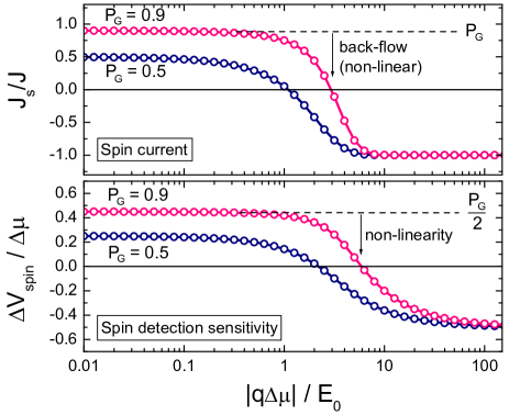
sensitivity as a function of is depicted in the bottom panel of figure 2. Indeed, for
small , the spin detection sensitivity is given by . However, the spin detection sensitivity
decays when the value of the spin splitting becomes large and approaches , and it even changes sign if
the spin splitting becomes much larger than . These two features are not obtained in linear transport
models, for which the spin detection sensitivity does not depend on the magnitude of the spin accumulation.
We emphasize that the change of the spin detection sensitivity is a consequence of the non-linearity
of the transport, i.e., it is not related to the back-flow of spins into the ferromagnet (see below).
The non-linearity will also cause the Hanle line shape to deviate from the typical Lorentzian variation as a function
of magnetic field, because the spin detection sensitivity changes as the spin accumulation is reduced. This
aspect is not explored any further here. It is also noteworthy that for reverse bias (), the spin detection
sensitivity goes to zero, since the reverse bias current is dominated by emission from the ferromagnet to the
semiconductor, which does not depend on , as already mentioned.
Next, we evaluate the spin current density. From equations (5) and (6) we obtain:
| (8) |
In the limit the spin current becomes:
| (9) |
The spin current is shown as a function of in the top panel of figure 2.
If the spin accumulation is small, the injected spin current is simply given by .
When the spin accumulation becomes larger and larger, the spin current is no longer independent
of and the existence of the spin accumulation reduces the injected spin current
(see Fig. 2, top panel). This phenomenon can be viewed as back-flow of spins into the
ferromagnetic electrode. Although this is well-established for linear
models fertprb ; fertieee ; jaffres ; maekawa ; dery the parameters that control it are
different here because the back-flow is non-linear (see below).
In principle, the spin current and the spin detection sensitivity of a ferromagnetic
Schottky contact can become negative due to the non-linearity (Fig. 2). However, an external (optical
or electrical) source of spins is needed to reach the regime with negative spin current and spin detection
sensitivity. If the same ferromagnetic contact is used to create and detect the spin accumulation, the detected
spin signal cannot change sign because the point where the spin detection sensitivity changes sign cannot
be reached. At very large density of injected current the spin accumulation becomes large, but during the
transient build up of the spin accumulation the injected spin current would first approach zero, and
beyond this point the spin accumulation does not increase any further. This saturation happens at a
value of the spin accumulation for which there is not yet a change in the sign of the spin detection
sensitivity (compare the zero-crossings in the bottom and top panels of Fig. 2).
III.2 Spin accumulation and Hanle spin signal
The steady-state spin accumulation is obtained by defining the relation between spin accumulation,
injected spin current and the spin resistance of the non-magnetic material in the usual jansensstreview
way (). If we insert expression (8) for the spin current into
this we do not obtain an analytic solution, but we can solve for numerically. The resulting
Hanle spin signal, the so-called spin RA product , is shown as a function of the contact
RA product in Fig. 3. At large contact resistance, the injected spin current is small
and so is the induced spin accumulation. In this regime back-flow is negligible and the spin RA product is
equal to , which is identical to the result of linear transport models. As the junction RA product is reduced
below a certain value, the spin RA product decays. This is due to the back-flow of spins into the ferromagnet,
which becomes important for large as it limits the injected spin current, as already eluded to.
Although this type behavior is also obtained for linear transport (see the solid black curve in Fig. 3),
the point where back-flow starts to become relevant is different. For linear transport, back-flow is
significant when the contact RA product is smaller than the spin resistance of the
semiconductor. However, for the non-linear transport considered here, the point where back-flow sets in is
shifted to contact resistances significantly larger than (Fig. 3, symbols). Thus, the non-linearity
enhances the back-flow and the contact resistance needed to avoid it is larger than for linear transport.
The value of for which back-flow sets in is of the order of a mV for the parameters used here
( meV). These features make the non-linearity relevant for the design of devices such as
spin transistors with a FM source and drain contact, since these typically require large spin accumulation
and small contact resistance to obtain a large magnetic response and high speed operation.

We can gain some additional insight by using the approximate expression (9) for the spin current in the weakly non-linear regime, for which an analytic solution for the spin accumulation can be obtained:
| (10) |
The term between brackets in equation (10) describes the reduction of the spin accumulation due to the back-flow. Whereas for linear transport this term is given by , we find that an additional factor appears. Since this factor is larger than unity for thermionic emission in the forward bias regime under consideration, the effective spin resistance that controls the back-flow is a factor of larger than .
III.3 Spin detection with a non-magnetic contact
A noteworthy aspect is that for a contact with a non-magnetic metal (), the spin current injected into the semiconductor is zero, but the spin-detection sensitivity is not (see figure 4). This is readily understood. If transport across the contact is non-linear, then the change in current induced by raising the electrochemical potential by for one spin direction is not compensated by the change in current due to the lowering of the electrochemical potential by for the other spin. The presence of a spin accumulation thus changes the total charge current across the contact. Hence, a non-magnetic contact with strongly non-linear transport can be used to electrically detect a spin accumulation (created by some external means, such as optically, or electrically from a nearby ferromagnetic injector). Note, however, that for a non-magnetic contact the sign of the spin voltage does not depend on the sign of , but is solely determined by the sign of the non-linearity (i.e., by the sign of the second derivative ). Also note that what we consider here is exclusively due to the non-linearity of the transport across the detector contact interface. It should be distinguished from effects due to the non-linearity of the transport within the non-magnetic channel, which in the presence of a spin accumulation has been shown to lead to charge voltages that can be detected by a contact with a non-magnetic electrode veramarun1 ; veramarun2 . This does not require nor rely on non-linear transport across the interface between the channel and the non-magnetic electrode. Similarly, the detection method we propose here does not require nor rely on non-linearity of the transport within the non-magnetic channel.

IV Discussion
Let us compare our results to previous works pu ; shiogai ; appelbaumdidv that consider
the effect of the non-linearity on the spin signals. Those previous descriptions do not include the ratio
of and and thus do not capture the associated physics. When is small,
the transport parameters are essentially constant in the energy window defined by the spin accumulation,
and this feature must be reflected in the description of the effect of the non-linearity on the spin signals.
Another notable feature of previous works pu ; shiogai is the appearance of a multiplicative
factor in the expression for the spin voltage pu ; shiogai ,
suggesting that spin signal enhancement occurs if the differential resistance is larger than the regular
resistance . Our results show that the effect of non-linearity on the magnitude of the spin signal
in general cannot be described by including this multiplicative factor (see also the appendix). In our
explicit evaluation the ratio of differential resistance and resistance does not appear, even though the transport by
thermionic emission is highly non-linear and rectifying note4 . Perhaps most strikingly, for reverse bias
the is much larger than , but the spin signal is not enhanced, and in
fact, the spin detection sensitivity goes to zero at reverse bias, as already noted in section IIIA.
Another example that shows that the magnitude of the spin signal does not track
is an Esaki diode. In the regime of negative differential resistance the Fermi level of the n-type
semiconductor is aligned with the band gap of the other (p-type) semiconductor. Creating a spin
splitting in the n-type semiconductor does not change the current because states around the Fermi
energy of the n-type electrode do not contribute to the current. Hence, the spin detection
sensitivity is zero. The differential resistance, however, is not zero. Hence, care should be taken
not to use the ratio of and in order to judge whether or not
the spin-detection sensitivity deviates from the linear result.
Let us finally discuss whether the transport non-linearity can enhance the detectable spin signal
and thereby explain the results of experiments on spin transport in FM/I/SC tunnel devices. For various
semiconductors (GaAs tran , Si jansennmatreview ; jansensstreview ; dash ; jeon ; uemura ; dashschottky ; sharmascaling ,
Ge saitoge ; jeonge ; jain ; ibage ; ibagert ; hanbickige ; jaingeinterface ; spiessergeox as well as oxide
semiconductors jaffresoxide ; parkinoxide ; dashoxide ) these devices exhibit Hanle spin signals that are orders
of magnitude larger than what is expected from the theory previously developed for spin injection into
non-magnetic metals fertprb ; fertieee ; jaffres ; maekawa ; dery . To explain the discrepancy, the role of
localized states in the tunnel oxide or at its interface with the semiconductor has been
considered tran ; jansentwostep ; derymr ; uemura ; casanova ; casanova2 . In particular,
spin transport by two-step tunneling via localized interface states was modeled and predicted to yield
greatly enhanced spin signals due to spin accumulation in those interface states tran . Because the
predictions of this model were shown to be inconsistent with experiments dash ; jansensstreview ; sharmascaling ,
extended versions derymr ; note1 ; casanova2 of the two-step tunneling model tran have recently been developed.
Nevertheless, some of the predictions of those extended models derymr ; casanova2 are also in
disagreement with experiments on electrical spin injection note2 and thermal spin injection by Seebeck
spin tunneling in similar FM/I/SC structures lebreton ; jainthermal ; jeonthermal ; jeonvoltage . The origin
of the large spin signals and whether localized states play a role is thus still unclear. With this
in mind, a recent experiment spiessermnge has focused on a direct Schottky
contact of a metallic ferromagnet (Mn5Ge3) and a semiconductor (Ge), in which the absence of a
tunnel oxide eliminates all sources of spin signal enhancement that rely explicitly on localized states
associated with the oxide tran ; jansentwostep ; derymr ; uemura ; casanova ; casanova2 . Nevertheless, the
observed spin signals spiessermnge , that have all the characteristic features of spin accumulation
and spin precession due to the Hanle effect, were found to be up to 4 orders of magnitude larger than
predicted by linear transport models fertprb ; fertieee ; jaffres ; maekawa ; dery . Since the studied
Mn5Ge3/Schottky contacts exhibited highly rectifying current-voltage characteristics, the question
arises whether the non-linear transport can affect the spin signal magnitude. Indeed, in some previous
reports it was argued that spin signals might be enhanced if transport is non-linear pu ; shiogai .
Our explicit evaluation shows that a spin signal enhancement due to non-linearity is unlikely.
First of all, our results show that in the regime where non-linearity is important (), the
effect is to reduce the spin detection sensitivity, not to enhance it. In fact, it is straightforward
to show that non-linearity in general reduces the spin detection sensitivity because current-voltage
characteristics are typically super-linear (i.e., the conductance increases
with bias voltage). The spin detection sensitivity is enhanced only in special cases where transport
is sub-linear. Secondly, even if non-linearity is present, the induced spin accumulation is generally
small enough to ensure that , in which case the spin current, spin-detection
sensitivity and spin voltage signal are well described by the expressions previously derived for linear
transport. For instance, for strongly rectifying transport by thermionic emission we have , but since
is typically a fraction of a meV in experiments conducted so far, the condition
is satisfied at the temperatures used in the experiments. For transport with
weaker rectification, the value of is larger, and the non-linearity is even less likely to
play a role. Nevertheless, non-linearity might become important for technologically relevant devices in
which contacts with large spin polarization and very small RA product are used and the spin accumulation
becomes large.
V Summary
The theory presented here serves as a basis for the interpretation of spin transport in rectifying ferromagnet/semiconductor Schottky contacts. It provides a quantitative means to assess whether non-linear transport modifies the spin current, spin-detection efficiency and the detectable spin voltage. The theory highlights the role of the magnitude of the induced spin splitting relative to the energy scale that parameterizes the degree of non-linearity. If the spin accumulation is large enough, the non-linearity is important, but it does not enhance the spin voltage. Rather, it reduces the spin-detection sensitivity. It also enhances the back-flow of spins into the ferromagnetic injector and its detrimental effect on the injected spin current. In order to suppress the back-flow, one needs a larger contact resistance than what is deduced from linear transport models. These results are relevant particularly for technological devices, since these generally require a large spin accumulation. It was also shown that the non-linearity enables a novel means to detect a spin accumulation in a semiconductor, using a non-linear contact with a non-magnetic metal electrode.
Appendix A Effect of non-linear conductance on spin-detection sensitivity
In this appendix we discuss how the non-linear conductance of a ferromagnetic contact affects
its spin-detection sensitivity, and in particular we examine whether or not the spin-detection sensitivity
is modified by a factor , as argued in previous works pu ; shiogai .
It is shown here that this multiplicative factor appears as a result of the (incorrect) assumption that the
non-linearity does not result in a change of the conductance when a spin accumulation is induced, but only
when the bias voltage changes.
In order to illustrate this, we consider transport that, to first order, is linear in the voltage
and incorporate the non-linearity by using a conductance that is a function of the
bias voltage and the spin accumulation. In the absence of a spin accumulation the voltage across
the contact is and the currents for each spin are simply given by:
| (11) | |||
| (12) |
where the denotes the conductance for and . The total current is then . In the presence of a non-zero spin accumulation, the voltage changes by an amount in order to keep the total current unchanged, and the currents become:
| (13) | |||
| (14) |
Importantly, the conductance deviates from not only because the voltage has changed by , but also because the electrochemical potential in the non-magnetic electrode is shifted by with respect to the average electrochemical potential (either up or down, depending on the spin orientation). In general and are small compared to , so that we can write:
| (15) | |||
| (16) |
From the requirement that the total current with and without spin accumulation is the same and equal to , and neglecting higher order terms proportional to , or , we obtain the voltage change as:
| (17) |
The extra factor between the straight brackets represents the modification of the spin-detection sensitivity
due to the non-linearity of the transport across the contact. In order to obtain the change in the spin-detection
sensitivity, one thus needs to evaluate the derivatives and ,
which depend on the particulars of the transport across the contact. It is instructive to consider the
spin-detection sensitivity for two limiting cases:
If , then
| (18) |
If , then
| (19) |
We thus find that the multiplicative factor of discussed in previous
works pu ; shiogai appears as a consequence of setting to zero.
In general this is not justified and as well as
are non-zero. For instance, a change in voltage across an oxide tunnel barrier will change the energy
of the tunneling electrons with respect to the maximum of the potential barrier and thereby changes
the tunnel conductance. However, when a spin accumulation is created, the associated shifts of the
electrochemical potential (up or down depending on the spin) also change the energy of the tunneling
electrons with respect to the barrier maximum and thus the conductance. Similar statements can be
made for tunneling through a Schottky barrier, where the effective width and height of the barrier
change upon application of a voltage but also upon creation of a spin accumulation.
While this does not mean that and are identical,
the non-zero counterbalances the effect of the non-zero .
This removes most of the multiplicative factor and yields a spin-detection
sensitivity that, despite the non-linearity, is close to the result obtained
for linear transport.
Note that the above analysis applies to systems in which transport to first order is linear, such as
tunneling transport. For thermionic emission over an energy barrier, as discussed in the main
text, the transport equations are different, and this needs to be considered when evaluating the spin-detection
sensitivity note0 .
References
- (1) C. Chappert, A. Fert and F. Nguyen van Dau, Nature Mater. 6, 813 (2007).
- (2) D. D. Awschalom and M. E. Flatté, Nature Phys. 3, 153 (2007).
- (3) A. Fert, Rev. Mod. Phys. 80, 1517 (2008).
- (4) R. Jansen, Nature Mater. 11, 400 (2012).
- (5) R. Jansen, S. P. Dash, S. Sharma, and B. C. Min, Semicond. Sci. Technol. 27, 083001 (2012).
- (6) G. Schmidt, D. Ferrand, L. W. Molenkamp, A. T. Filip, and B. J. van Wees, Phys. Rev. B 62, R4790 (2000).
- (7) A. Fert and H. Jaffrès, Phys. Rev. B 64, 184420 (2001).
- (8) S. Takahashi and S. Maekawa, Phys. Rev. B 67, 052409 (2003).
- (9) A. Fert, J.-M. George, H. Jaffrès, and R. Mattana, IEEE Trans. Elec. Dev. 54, 921 (2007).
- (10) H. Jaffrès, J.-M. George, and A. Fert, Phys. Rev. B 82, 140408 (2010).
- (11) Y. Song and H. Dery, Phys. Rev. B 81, 045321 (2010).
- (12) H. Dery and L. J. Sham, Phys. Rev. Lett. 98, 046602 (2007).
- (13) R. Jansen and B. C. Min, Phys. Rev. Lett. 99, 246604 (2007).
- (14) M. Tran, H. Jaffrès, C. Deranlot, J.-M. George, A. Fert, A. Miard, and A. Lemaître, Phys. Rev. Lett. 102, 036601 (2009).
- (15) R. Jansen, A. M. Deac, H. Saito, and S. Yuasa, Phys. Rev. B 85, 134420 (2012).
- (16) Y. Song and H. Dery, Phys. Rev. Lett. 113, 047205 (2014).
- (17) Just as in the original model by Tran et al. tran , the refined model by Song and Dery derymr relies on transport in two steps via localized states in the junction, the current induces a spin-polarized occupation of the localized states, and spin precession and the Hanle effect produce the change of the voltage in an external magnetic field.
- (18) T. Tanamoto, M. Ishikawa, T. Inokuchi, H. Sugiyama, and Y. Saito, J. Appl. Phys. 115, 163907 (2014).
- (19) J. Ghosh, V. Sverdlov, T. Windbacher, and S. Selberherr, J. Appl. Phys. 115, 17C503 (2014).
- (20) Y. Pu et al., Appl. Phys. Lett. 103, 012402 (2013).
- (21) J. Shiogai, M. Ciorga, M. Utz, D. Schuh, M. Kohda, D. Bougeard, T. Nojima, J. Nitta, and D. Weiss, Phys. Rev. B 89, 081307 (2014).
- (22) H. N. Tinkey, P. Li, and I. Appelbaum, Appl. Phys. Lett. 104, 232410 (2014).
- (23) S.M. Sze, ”Physics of semiconductor devices” (Wiley, New York, 1981).
- (24) The application of a bias voltage modifies not only the height of the barrier as seen by electrons in the semiconductor, but also the barrier width, whereas the spin accumulation only changes the height of the barrier by an amount depending on the spin. Nevertheless, shifting the electrochemical potential by a spin accumulation or by a voltage has the same affect on the thermionic emission current, because thermionic emission is well-described by a theory in which only the height of the barrier is considered, and not its detailed shape.
- (25) I. J. Vera-Marun, V. Ranjan, and B. J. van Wees, Phys. Rev. B 84, 241408 (2011).
- (26) I. J. Vera-Marun, V. Ranjan, and B. J. van Wees, Nature Phys. 8, 313 (2012).
- (27) The nonlinearity of thermionic emission arises because transport is determined by electrons in the high energy tail of the electron distribution, whose density depends exponentially on energy. Since shifting the electrochemical potential by a spin accumulation or by a voltage has the same affect on the thermionic emission current note0 it follows that the spin detection sensitivity does not depend on the ratio of differential resistance and resistance. When a spin accumulation is induced, the resulting current change is inversely proportional to the differential resistance. In order to keep the current constant, the voltage across the junction has to change, but this change is proportional to the same differential resistance. Hence, the value of the differential resistance is immaterial.
- (28) S. P. Dash, S. Sharma, R. S. Patel, M. P. de Jong, and R. Jansen, Nature 462, 491 (2009).
- (29) K. R. Jeon, B. C. Min, I. J. Shin, C. Y. Park, H. S. Lee, Y. H. Jo, and S. Ch. Shin, Appl. Phys. Lett. 98, 262102 (2011).
- (30) T. Uemura, K. Kondo, J. Fujisawa, K. Matsuda, and M. Yamamoto, Appl. Phys. Lett. 101, 132411 (2012).
- (31) A. Dankert, R. S. Dulal, and S. P. Dash, Sci. Rep. 3, 3196 (2013).
- (32) S. Sharma, A. Spiesser, S. P. Dash, S. Iba, S. Watanabe, B. J. van Wees, H. Saito, S. Yuasa, and R. Jansen, Phys. Rev. B 89, 075301 (2014).
- (33) H. Saito, S. Watanabe, Y. Mineno, S. Sharma, R. Jansen, S. Yuasa, and K. Ando, Solid State Comm. 151, 1159 (2011).
- (34) K. R. Jeon, B. C. Min. Y. H. Jo, H. S. Lee, I. J. Shin, C. Y. Park, S. Y. Park, and S. Ch. Shin, Phys. Rev. B 84, 165315 (2011).
- (35) A. Jain et al., Appl. Phys. Lett. 99, 162102 (2011).
- (36) S. Iba, H. Saito, A. Spiesser, S. Watanabe, R. Jansen, S. Yuasa, and K. Ando, Appl. Phys. Express 5, 023003 (2012).
- (37) S. Iba, H. Saito, A. Spiesser, S. Watanabe, R. Jansen, S. Yuasa, and K. Ando, Appl. Phys. Express 5, 053004 (2012).
- (38) A. T. Hanbicki, S. F. Cheng, R. Goswami, O. M. J. van ’t Erve, and B. T. Jonker, Solid State Commun. 152, 244 (2012).
- (39) Jain, A. et al., Phys. Rev. Lett. 109, 106603 (2012).
- (40) A. Spiesser, S. Watanabe, H. Saito, S. Yuasa, and K. Ando, Jap. J. Appl. Phys. 52, 04CM01 (2013).
- (41) Reyren, N. et al., Phys. Rev. Lett. 108, 186802 (2012).
- (42) W. Han, X. Jiang, A. Kajdos, S.-H. Yang, S. Stemmer, and S. S. P. Parkin, Nature Commun. 4, 2134 (2013).
- (43) A. M. Kamerbeek, E. K. de Vries, A. Dankert, S. P. Dash, B. J. van Wees, and T. Banerjee, Appl. Phys. Lett. 104, 212106 (2014).
- (44) O. Txoperena, M. Gobbi, A. Bedoya-Pinto, F. Golmar, X. Sun, L. E. Hueso, and F. Casanova, Appl. Phys. Lett. 102, 192406 (2013).
- (45) O. Txoperena, Y. Song, L. Qing, M. Gobbi, L. E. Hueso, H. Dery, and F. Casanova, arXiv:1404.0633 (2014).
- (46) The predictions of the model by Song and Dery derymr seem to be in disagreement with existing experiments jansensstreview ; dash ; jeon ; spiessergeox in which no significant reduction of the spin signal is observed when the bias voltage is changed from the regime with to the regime with . The current modulation that Song and Dery describe relies on the condition . Because of this condition, the relevant states in the emitting electrode remain fully occupied, so that after an electron has tunneled for instance from the non-magnetic electrode into a localized state in the barrier, the transport back into the non-magnetic electrode is completely blocked. However, for , the relevant states around the Fermi energy of the emitting electrode are not fully occupied and transport back into the emitter is not blocked. Consequently, the current modulation that Song and Dery describe is expected to be reduced in a region having a width of a few around zero bias voltage. Experimentally this is not observed jansensstreview ; dash ; jeon ; spiessergeox . Moreover, because the model by Song and Dery relies on the condition that , it cannot account for the obervation of thermally-driven spin injection without a charge tunnel current by Seebeck spin tunneling lebreton ; jainthermal ; jeonthermal ; jeonvoltage .
- (47) J.C. Le Breton, S. Sharma, H. Saito, S. Yuasa, and R. Jansen, Nature 475, 82 (2011).
- (48) A. Jain et al., Appl. Phys. Lett. 101, 022402 (2012).
- (49) K.-R. Jeon et al., Sci. Rep. 2, 962 (2012).
- (50) K.-R. Jeon et al., Nature Mater. 13, 360 (2014).
- (51) A. Spiesser, H. Saito, R. Jansen, and S. Yuasa, Phys. Rev. B 90, 205213 (2014) [and arXiv:1410.4277].