Engineering semiconductor hybrids for sensing
Abstract
The effect of screening of the coulomb interaction between two layers of two-dimensional electrons, such as in graphene, by a highly doped semiconducting substrate is investigated. We employ the random-phase approximation to calculate the dispersion equation of this hybrid structure in order to determine the plasmon excitation spectrum. When an electric current is passed through a layer, the low-frequency plasmons in the layer may bifurcate into separate streams due to the current-driving effect. At a critical wave vector, determined by the separation between layers and their distance from the surface, their phase velocities may be in opposite directions and a surface plasmon instability leads to the emission of radiation. Applications to detectors and other electromagnetic devices exploiting nano-plasmonics are discussed.
pacs:
73.21.-b, 71.70.Ej, 73.20.Mf, 71.45.Gm, 71.10.Ca, 81.05.UeI Introduction and formalism
Rapid progress has been made in recent years in combining two or more different types of materials to form hybrid nanoparticles on the same nanosystem new1 ; new2 ; new3 ; new4 ; new5 ; new6 ; new7 ; new8 ; new9 ; new10 . The main goal of these endeavors is to produce unusual materials with desired functionality such as sensors. Examples include inorganic cage structures obtained by a selective edge growth mechanism of the metal onto the semiconductor nanocrystal. Successful approaches now exist for synthesizing composites with a high degree of control over their shapes, compositions and interfacial properties. The advances in architecture are very impressive and the resulting advanced materials are now being investigated for application of hybrid nanoparticles in electronic devices such as a microlaser, optical components, catalysis, and photocatalysis. A necessary condition for efficient operation of these composite structures is electronic coupling across the constituent interfaces.
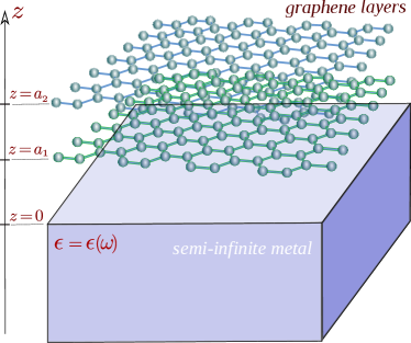
This paper focuses on a doped two-dimensional (2D) semiconductor layer hybrid nanoparticle structure for which there is a high degree of control over its performance as a source of electromagnetc radiation. We point out some challenges for further understanding and development of semiconductor-metal hybrid nanoparticles. Specifically, we consider a composite nano-system as shown in Fig.[ 1] consisting of a thick layer of conducting substrate on whose surface the plasmon is activated in proximity with a pair of thin layers. We demonstrate how the screening of the Coulomb coupling of the plasmons in this pair of layers by the charge density fluctuations on the surface of a semi-infinite substrate affects the surface plasmon instability that leads to the emission of radiation (spiler). The excitation of these plasmon modes is induced by resonant external optical fields. As an emitter, the spiler may be activated optically. Spiler exploits the flexibility of choosing its constituents to produce coherent sources of radiation. Applications to photodetectors and electromagnetic-wave devices exploiting nano-plasmonics are explored.
Our approach models an ensemble consisting of a pair of 2D layers and a thick layer of a conducting medium that emits radiation when an electric field splits the plasmon spectrum which results in an instability as the phase velocities associated with these plasmon branches have opposing signs at a common frequency.
In our formalism, we consider a nano-scale system consisting of a pair of 2D layer structure with a double layer positioned at and () and a thick conducting material. The layer may be monolayer graphene or a 2D electron gas (2DEG), such as a semiconductor inversion layer or a high electron mobility transistor. The graphene layer may have a gap, thereby extending the flexibility of the composite system that also incorporates a thick layer of conducting material as depicted in Fig. 1. The excitation spectra of allowable modes will be determined from the solutions of the dispersion equation which includes the screened Coulomb coupling between layers and between each layer and the semi-infinite substrate. Following standard procedures within the random-phase approximation (RPA) Arxiv ; Tso , calculation shows that the plasmon dispersion equation is , where
| (1) | |||||
whose is the 2D polarization function and is the bulk plasma frequency of the semi-infinite medium. In our numerical calculations, we employ . For a 2DEG, we have with electron density and electron effective mass . For graphene, we find
| (2) |
where is the chemical potential and is the induced gap between valence and conduction bands. Then, we obtain a quartic equation in . The plasmon frequencies in this approximation are
| (3) | |||
where . Here, in our notation, for . The spectral function yields real frequencies. A 2D layer interacting with the half-space has two resonant modes. Each pair of 2D layers interacting in isolation far from the half-space conducting medium supports a symmetric and an antisymmetric mode DasSarma . In the absence of a driving current, the analytic solutions for the plasmon modes for a pair of 2D layers that are Coulomb coupled to a half-space are given by the term which plays the role of “Rabi coupling”. Clearly, for long wavelengths, only depends on . However, the excitation spectrum changes dramatically when a current is driven through the configuration. Under a constant electric field, the carrier distribution is modified, as may be obtained by employing the relaxation time approximation in the equation of motion for the center-of-mass momentum. For carriers in a parabolic energy band with effective mass and drift velocity determined by the electron mobility and the external electric field, the electrons in the medium are redistributed. This is determined by a momentum shift in the electron wave vector in the thermal-equilibrium Fermi function . By making a change of variables in the well-known Lindhard polarization function , this effect is equivalent to a frequency shift . For massless Dirac fermions in graphene with linear energy dispersion, this Doppler shift in frequency is not in general valid for arbitrary wave vector. This is our conclusion after we relate the surface current density to the center-of-mass wave vector in a steady state. Our calculation shows that the redistribution of electrons leads to a shift in the wave vector appearing in the Fermi function by the center-of-mass wave vector where and are the Fermi wave vector and velocity, respectively. However, in the long wavelength limit, , the Doppler shift in frequency is approximately obeyed. Consequently, regardless of the nature of the 2D layer represented in the dispersion equation we may replace in the dispersion equation in the presence of an applied electric field at long wavelengths.
II Numerical Results and Discussion
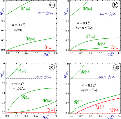
We shall treat the solution frequencies as complex variables with , where implies finite growth rates for two split plasmon modes. Since is a complex function, we ask for . Therefore, we are left with damping-free plasmon modes in the spatial domain in the system but they still face possible instability in the time domain due to .
The number of plasmon excitation branches for chosen as well as the instability domain depends on the magnitude of the drift current and also on the distance between the constituents of the hybrid system. In Fig: 2, we show the complex plasma frequency solutions of our dispersion equation, with the real parts representing the dispersion, and the imaginary part corresponding to the rate of growth of the instability (inverse of ). For a hybrid system made up of a semi-infinite heavily doped semiconductor and a 2D layer, we obtain two plasmon frequency solutions in the absence of a current. As the current is increased, another solution with positive real part of the frequency may be determined, but there may be no imaginary part of this solution until the current reaches a critical value. The instability is closely connected to the observed closed loop of the real solution. Mathematically, it could be explained by the fact that for an even power equation with real coefficients for zero current all the solutions must be complex conjugated, e.g., have identical real parts.
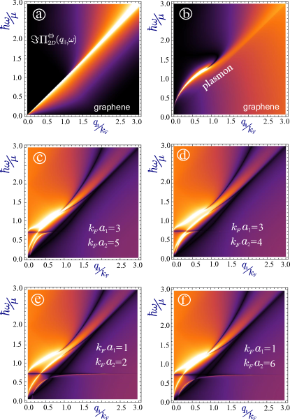
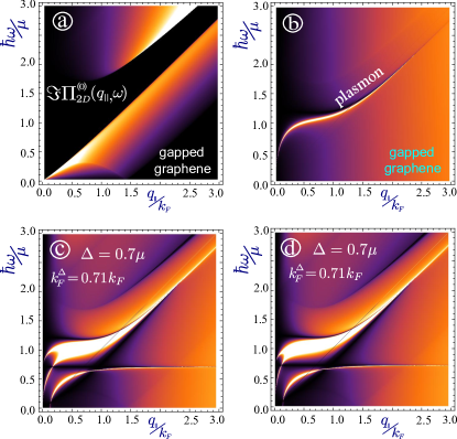
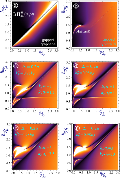
We now turn to discuss the plasmon dispersion for a hybrid semi-infinite conductor and two layers of graphene, both with and without an energy gap. First, we investigate the single-particle excitation region responsible for Landau damping, outside of which undamped plasmons could be observed. The regions of the undamped plasmons is given by solving . The results are presented in Fig. 3(a) for gapless grpahene, and in Figs. 4(a) and 5(a) for large () and small () energy band gap. Next, we show the plasmon in a single graphene layer for each case DasSarma ; wunsch ; pavlo . If there is no energy gap [see Fig. 3(b)] or its value is small (compared with the chosen gap) in Fig. 5(b), the plasmon is undamped only for a small range of . In contrast, for large energy gap, Fig. 4(b) shows that an undapmed plasma is found for a larger range of the wave vector.
Finally, we consider the plasmon dispersion when there are two 2D layers and a semi-infinite conductor with free carriers. Our solutions are determined by the location of the particle-hole mode regions for each case, so that we obtain longer undamped plasmon branches for the case of gapped graphene, shown in Figs. [4](c) and (d). The distance between the surface and each of the 2D layers is also an important factor. When the larger distance is chosen, the middle plasmon branch, i.e., the one which starts from the origin with a bigger slope, tends to get close to coincide with the the uppermost branch, which starts from . For finite energy gap, the ‘surface’ plasmon mode shows much brighter and broader peak, compared to the lowest branch as depicted in Figs. 4(b)-4(d) and Figs. 5(c)-5(f).
III Concluding Remarks
In summary, we are proposing a hybrid quantum plasmonic device which employs 2D layers in combination with a thick conducting material. We find that the spiler emits electromagnetic radiation when a current is passed through the 2D layer to make the plasmons become unstable at a specific frequency and wave number and grow over a period of time which is determined by the positive imaginary part of its complex frequency. It is possible to change the range of plasmon instability by selecting the properties of the nanosheet or frequency of the surface plasmon, i.e., the substrate. The surface plasmon plays a crucial role in giving rise to the Rabi-like splitting and the concomitant streams of quasiparticles whose phase velocities are in opposite directions when the instability takes place. The emitted electromagnetic radiation may be collected from regions on the surface that are convenient.
Promising sources of terahertz (THz) radiation have been investigated over the years. These frequencies cover the electromagnetic spectrum from microwave to infrared. Epitaxial growth of hybrid layers of semiconductors resulted in quantum well structures emitting high power THz across a wide frequency range. So far, only ultra-long wavelength emission has been reported. Our work shows how we may modify this limitation with the use of the proposed hybrid structure through a spontaneous generation of plasmon excitations and subsequent Cherenkov radiation at sufficiently high draft velocities.
Acknowledgements.
This research was supported by contract # FA 9453-13-1-0291 of AFRL. DH would like to thank the Air Force Office of Scientific Research (AFOSR) for its support.References
- (1) U. Banin, Y. Ben-Shahar, and K. Vinokurov, Chem. Mater. 26, 97 (2014).
- (2) K. A. Brown, Q. Song, D. W. Mulder, and P. W. King, ACS Nano (2014) [DOI: 10.1021/nn504561v].
- (3) P. S. Dilsaver, M. D. Reichert, B. L. Hallmark, M. J. Thompson, and J. Vela, J. Phys. Chem. C 118, 21226 (2014).
- (4) N. Liakakos, C. Gatel, T. Blon, T. Altantzis, S. Lentijo-Mozo, C. Garcia-Marcelot, L.-M. Lacroix, M. Respaud, S. Bals, G. Van Tendeloo, and K. Soulantica, Nano Lett. 14, 2747 (2014).
- (5) L. J. Hill, N. E. Richey, Y. Sung, P. T. Dirlam, J. J. Griebel, E. Lavoie-Higgins, I.-B. Shim, N. Pinna, M.-G. Willinger, W. Vogel, J. J. Benkoski, K. Char, and J. Pyun, ACS Nano 8, 3272 (2014).
- (6) X. Ye, D. R. Hickey, J. Fei, B. T. Diroll, T. Paik, J. Chen, and C. B. Murray, J. Am. Chem. Soc. 136, 5106 (2014).
- (7) S. Blumstengel, S. Sadofev, C. Xu, J. Puls, R. L. Johnson, H. Glowatzki, N. Koch, and F. Henneberger, Phys. Rev. B77, 085323 (2008).
- (8) M. Fu, K. Wang, H. Long, G. Yang, P. Lu, F. Hetsch, A. S. Susha, and A. L. Rogach, Appl. Phys. Lett. 100, 063117 (2012).
- (9) J. A Kurzman, M.-S. Miao, and R. Seshadri, J. Phys.: Condens. Matt. 23, 465501 (2011).
- (10) G. Wang, X. Jiang, M. Zhao, Y. Ma, H. Fan, Q. Yang, L. Tong, and M. Xiao, Opt. Expr. 20, 29472 (2012).
- (11) G. Gumbs, A. Iurov, and D. H. Hunag, arXiv:1410.2851 [cond-mat.mtrl-sci] (2014).
- (12) N. J. M. Horing, H. C. Tso, and G. Gumbs, Phys. Rev. B36, 1588 (1987).
- (13) S. Das Sarma and A. Madhukar, Phys. Rev. B23, 805 (1981).
- (14) B. Wunsch, T. Stauber, F. Sols, and F. Guinea, New J. Phys. 8, 318 (2006).
- (15) P. K. Pyatkovskiy, J. Phys.: Condens. Matt. 21, 025506 (2009).