A high-mobility electronic system at an electrolyte-gated oxide surface
Electrolyte gating is a powerful technique for accumulating large carrier densities in surface two-dimensional electron systems (2DES) Fujimoto2013 . Yet this approach suffers from significant sources of disorder: electrochemical reactions can damage or alter the surface of interest Schladt2013 ; Jeong2013 ; Li2013 ; Petach2014 , and the ions of the electrolyte and various dissolved contaminants sit Angstroms from the 2DES. Accordingly, electrolyte gating is well-suited to studies of superconductivity Ueno2008 ; Ueno2011 ; Ye2012 and other phenomena robust to disorder, but of limited use when reactions or disorder must be avoided. Here we demonstrate that these limitations can be overcome by protecting the sample with a chemically inert, atomically smooth sheet of hexagonal boron nitride (BN). We illustrate our technique with electrolyte-gated strontium titanate, whose mobility improves more than tenfold when protected with BN. We find this improvement even for our thinnest BN, of measured thickness 6 Å, with which we can accumulate electron densities nearing cm-2. Our technique is portable to other materials, and should enable future studies where high carrier density modulation is required but electrochemical reactions and surface disorder must be minimized.
A conventional field-effect transistor is controlled by the voltage on a metal electrode separated from the channel by a thin insulating dielectric. The maximum applied voltage is determined by the dielectric breakdown field, beyond which the resistance of the dielectric sharply drops, shorting the metal electrode to the channel. For a typical high-quality dielectric, the breakdown field limits the accumulated carrier density to cm-2 (Ref. 9), although for special cases such as ferroelectrics stronger modulation is possible Ahn1999 ; Takahashi2006 ; Boucherit2014 . Electrolyte gating circumvents dielectric breakdown by eliminating the metal/dielectric interface: an electrolyte is applied directly to the surface of interest and polarized, drawing one charged species to the surface and building a large electric field. Carrier densities cm-2 can be induced by electrolyte gating Yuan2009 , facilitating the discovery of superconductivity in new parameter regimes Ueno2011 ; Ye2012 and the creation of novel photonic devices Zhang2014 , among other advances.
While very effective at modulating surface properties, electrolyte gating also introduces disorder. The deposition of contaminants on the sample is difficult to control, a problem that is compounded by the possibility of surface-degrading electrochemical reactions. Recent studies have further suggested that chemical modification of the surface of interest, rather than electrostatics, is primarily responsible for the dramatic changes in electronic properties in some electrolyte-gated systems Schladt2013 ; Jeong2013 ; Petach2014 . Motivated by these challenges, we consider the well-studied 2DES created by electrolyte gating at the surface of strontium titanate (STO) Ueno2008 ; Ueno2010 ; YLee2011 ; MLee2011 ; Li2012 ; Stanwyck2013 ; Ueno2014 . The transport properties of this surface 2DES closely resemble those of the 2DES at the lanthanum aluminate/strontium titanate (LAO/STO) interface. However, the highest reported low-temperature electron mobility in the STO 2DES is about 1000 cm2V-1s-1, at an electron density of cm-2 (Ref. 6, 15, 17, 20); for the same density, the LAO/STO 2DES has mobility up to cm2V-1s-1 (Ref. 21). We demonstrate that by protecting the STO channel with a thin boron nitride dielectric, the mobility of the resulting electrolyte-gated 2DES substantially increases over a wide density range, surpassing cm2V-1s-1 at a density of cm-2 in our best sample.
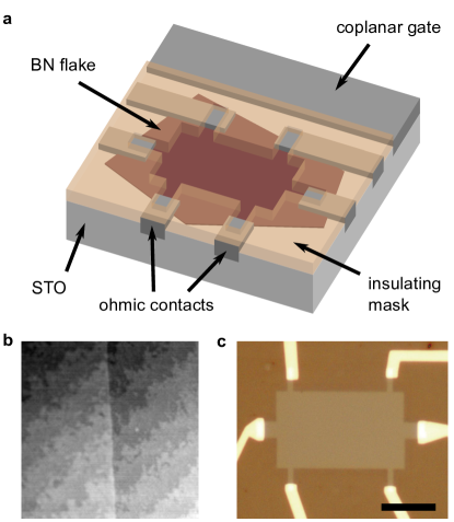
Each of our samples consists of a single crystal of STO partially covered by an atomically-flat BN flake (Fig. 1a). The BN flake conforms to the substrate without trapping contaminants, as evidenced by the 4 Å terrace steps of the underlying STO seen in the topography of the BN (Fig. 1b). The substrate is masked by a thick insulator except in a Hall bar-shaped channel area (Fig. 1c); the electrolyte induces negligible carrier density in the masked regions. In this work, we consider four BN-covered STO samples–denoted A, B, C, and D–with BN thicknesses measured to be 0.6, 1.0, 1.2, and 1.5 nm, respectively, by atomic force microscopy (see Supplementary Information for lateral dimensions and thickness measurement details). For each sample, we collect low-temperature magnetotransport data over multiple cooldowns at different coplanar gate voltages .
The striking improvement in 2DES quality with a BN spacer is evident in the magnetotransport properties of Sample A, which is covered by a 6 Å-thick flake (Fig. 2a,b). The five cooldowns of Sample A, numbered 1 through 5, correspond to different settings. Although higher typically induces higher density, this is not always the case because of hysteresis (see Methods) and because of drifting offset voltages from electrochemical reactions at the gate electrode. To extract density and mobility, we perform a simultaneous fit to the sheet resistance and the Hall coefficient , where is the Hall resistance, is the magnetic constant, and is the applied magnetic field. As is typical in the STO 2DES literature, we assume that the magnetotransport behavior can be described by two bands Joshua2012 . Although quantum oscillation data suggest several bands (discussed below), a two-band description often fits the data, providing reliable numbers for average mobility and total density (Supplementary Information). For LAO/STO, a two-band fit with four parameters (densities , , mobilities , ) captures the approximate shapes of and , but deviates from the data at higher fields Joshua2012 . We encounter the same difficulty: the two-band model cannot simultaneously fit the nonsaturating linear magnetoresistance and nearly-saturated Hall coefficient observed up to 31 T in our samples (Supplementary Information) and in LAO/STO samples BenShalom2010 . Inclusion of a third band cannot generally reproduce our high-field data, and where a three-band fit does work, the required densities are unrealistically large, frequently exceeding cm-2 with mobility cm2V-1s-1. We instead fit to a two-band model in which the sheet resistance of each band contains a term linear in applied field: for and . The linear term could arise from spatial fluctuations in mobility Parish2003 ; Kozlova2012 .
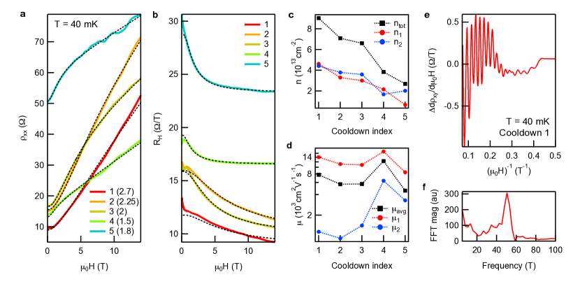
Our two-band fits with linear magnetoresistance provide an excellent match to the data (Fig. 2a,b). These fits exclude the low-field region, where the magnetotransport properties are affected by magnetic moments in the STO (Ref. 26 and Supplementary Information). We find a high-mobility band with density between and cm-2 (Fig. 2c) and mobility between 8000 and 17000 cm2V-1s-1 (Fig. 2d), as well as a low-mobility band with a similar density and mobility that grows with decreasing . The total induced density can reach cm-2 (Fig. 2c) with an average mobility approaching 8000 cm2V-1s-1 (Fig. 2d). The average mobility for Cooldown 4 exceeds 12000 cm2V-1s-1. These mobilities match (for lower densities) and exceed (for higher densities) the highest reported mobilities in LAO/STO 2DES Huijben2013 ; Xie2013 , and are ten times larger than the mobilities reported in the literature for electrolyte-gated STO 2DES at any carrier density Ueno2008 ; Ueno2010 ; Ueno2014 . Our conclusions are unchanged if we instead calculate and by naively dividing by , or if we fit with the four-parameter, two-band model (Supplementary Information).
Quantum oscillations appear above T in both and for all cooldowns. The oscillations from Cooldown 1 (Fig. 2e) show a primary oscillation frequency of 50 T (Fig. 2f), corresponding to a carrier density near cm-2. This contrasts with the results of the two-band Hall transport fits, in which both bands are at least ten times more populated. For a typical cooldown, we can identify multiple quantum oscillation frequencies corresponding to densities cm-2, regardless of the total density measured by the Hall effect. The strongest oscillations thus appear for the lowest Hall densities (see Cooldown 5 in Fig. 2a), as the bands that produce quantum oscillations now constitute a substantial fraction of the carriers. Our findings resemble quantum oscillation data collected on the highest-mobility LAO/STO 2DES, in which multiple bands of density cm-2 show quantum oscillations, and total Hall densities cm-2 or lower are required for strong oscillations in (Ref. 28, 29). The presence of low-density oscillating bands does not strongly impact the shapes of and , so the two-band model still captures most of the device behavior (Supplementary Information).
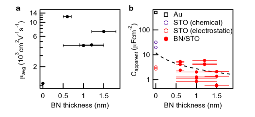
The maximum mobility that we have achieved in each of our four BN-covered samples is significantly higher than the maximum mobility that we have achieved in any uncovered STO sample (Fig. 3a). The mobility improvement with BN results in part from the added separation between the 2DES and the disordered charges in the electrolyte. As discussed below, we also expect that the BN acts as a barrier to surface-degrading chemical reactions that occur during electrolyte gating or during processing. Our limited sample size produces enough scatter in the maximum mobility as a function of thickness that we cannot identify the main sources of residual disorder.
A single layer of graphene is known to be permeable to atomic hydrogen Waqar2007 but impermeable to other small chemical species, including He atoms Bunch2008 and Li+ ions Das2013 . Because BN has a lattice structure nearly identical to that of graphene, we anticipate a similar diffusion resistance for even our thinnest BN barriers. The energy barrier to diffusion is so high (Ref. 32 calculates 10 eV for Li+ across graphene) that we still expect impermeability with dropped across our BN. An electrolyte-gated gold sample covered by 6 nm of BN behaved in accordance with these expectations: a gold oxide film is readily grown on uncovered gold samples Petach2014 , but the BN-covered gold sample was unmodified (Supplementary Information). The chemical species responsible for the redox reaction is unknown, but these results nonetheless illustrate that BN can limit chemical reactions during electrolyte gating.
An intriguing possibility for electrolyte-gated oxides is that BN barriers could prevent oxygen removal. Experiments on rutile TiO2 single crystals Schladt2013 and VO2 thin films Jeong2013 have found evidence that oxygen near the crystal surface diffuses out through the electrolyte, calling into question the relative roles of oxygen vacancy creation and electrostatic carrier accumulation in tuning sample properties. An electrolyte-gating study of STO found that injecting oxygen gas into the electrolyte suppresses the source-drain current, which was interpreted as evidence that the otherwise-observed carrier accumulation results from oxygen vacancies Li2013 . Another study of STO concluded that very high gate voltages are required to create oxygen vacancies, and that the reduced STO system (density cm-2) is three-dimensional and remains conductive at zero gate voltage Ueno2010 . While we cannot directly prove the absence of oxygen migration when gating BN-protected STO, we verify that electrostatic carrier accumulation can account for our data by considering the apparent capacitance between the electrolyte and the 2DES, defined as . If electrostatics alone is responsible for the carrier accumulation, should fall below a serial arrangement of two capacitances: that of the double layer formed by the ions (, Ref. 33), and that of the BN dielectric. This yields , where 4 is the dielectric constant of BN and is the sheet thickness. On the other hand, if carriers accumulate by chemical modification, is unrestricted.
For all BN-covered samples, falls near or below , and two orders of magnitude below for uncovered gold, whose surface is chemically modified by electrolyte gating Petach2014 . The capacitance to the channel from the large coplanar gate, located less than 200 m away, accounts for the violation of the electrostatic limit in Samples A (0.6 nm) and C (1.2 nm). Due to the low-temperature dielectric constant of 25000 in STO and the focusing of field lines from the large gate onto the much smaller Hall bar Rakhmilevitch2013 , this capacitance can be as large as several Fcm-2. We have measured such a capacitance on some samples by zeroing the coplanar gate voltage at low temperature. However, modulating the gate voltage at low temperature appears to cause mechanical problems as our ionic liquid droplet unfreezes upon warmup. We therefore did not collect coplanar gate capacitance data for most samples, and cannot quantitatively correct .
Our device geometry exposes some area of our contact metal directly to the electrolyte (Fig. 1a), limiting to about 3 V: above this, chemical reactions readily occur with the contact metal. This limitation in turn limits the maximum thickness of BN that can be used to create a metallic STO 2DEG. The lowest density for which we have measured a conducting state in our STO 2DES is cm-2, although the mobility edge may be somewhat lower. To accumulate cm-2 electrostatically requires a minimum capacitance of 0.5 Fcm-2, or a maximum BN thickness of 7 nm. Although we have not studied such thick BN flakes, we have measured several samples which had wrinkles in the BN several nm tall due to the transfer process (Supplementary Information). When these wrinkles cut fully across the current path between source and drain, the sample never conducted between source and drain. Presumably the area beneath the wrinkles remained insulating, in approximate numerical agreement with the electrostatic accumulation picture.
The BN barrier need not be kept thin if all conductive material can be masked. This is often difficult in insulators, since the electrolyte must create a conductive path between the device channel and metal contacts, unless the insulator can be chemically doped near the contacts. For intrinsically metallic systems, it is straightforward to mask all conductive area (see our BN on gold sample, Supplementary Information). In this case, higher voltages can in principle be applied without chemical reactions, increasing the maximum thickness of BN that can be used for a target electron density, which may have advantages for certain materials. Our technique is easily applied to other systems, and should enable electrolyte gating experiments that require high carrier mobility, high carrier density, and chemical stability of the surface.
Methods
Our samples were fabricated on (100) strontium titanate substrates from either Shinkosha Co. (Japan) or Crystec GmbH (Germany); the vendor for each sample is specified in the Supplementary Information. The surfaces of Shinkosha crystals were TiO2-terminated as received. We prepared a nominally TiO2-terminated surface on the Crystec samples by the method described in Ref. 35. A BN flake was transferred onto the STO surface using the water-based process described in Ref. 36, followed by an anneal for 4 hours at 500°C in an Ar/O2 atmosphere. An ohmic contact pattern was defined in PMMA via e-beam lithography at 10 kV, after which the sample was milled with Ar ions at 300 V to etch away the exposed BN and about 40 nm of the underlying STO. Ohmic contacts (10 nm titanium, 40 nm gold) were then deposited into the milled trenches by e-beam evaporation. Finally, an insulating mask with holes to expose the Hall bar and the coplanar gate was patterned using 10 kV e-beam lithography. The mask material was either crosslinked PMMA or sputtered alumina; in both cases a negative process was used so that the channel was not exposed to the e-beam.
Prior to measurement of each sample, we cleaned the sample surface of resist residues by a brief exposure to a remote oxygen plasma. We then covered the Hall bar and coplanar gate with a drop of the ionic liquid 1-ethyl-3-methylimidazolium bis(trifluoromethanesulfonyl)amide (EMI-TFSI) and placed the sample inside the vacuum chamber of our cryostat (either a dilution refrigerator with base temperature 40 mK or a variable-temperature insert reaching 350 mK or 1.5 K). We polarized the electrolyte at around 290 K, in either high vacuum or helium vapor, by applying a voltage to the coplanar gate. Upon cooling, the polarized electrolyte froze, and we collected magnetotransport data up to the highest available fields (9 T, 14 T, or 31 T) via standard lock-in techniques in a current-biased configuration. We typically used an ac source current of 2 A, which exceeded the superconducting critical current in all samples, suppressing the superconducting features that would otherwise appear for some cooldowns in Fig. 2. The sample was then warmed to near room temperature, melting the electrolyte. We always set to zero in between cooldowns, which introduces some hysteresis in .
Acknowledgements
We thank Thomas Schladt and Tanja Graf for helpful discussions at an early stage of this work, and Harold Hwang for a careful reading of our manuscript. Sample fabrication was supported by the Air Force Office of Science Research, Award No. FA9550-12-1-02520. Sample measurement was supported by the MURI program of the Army Research Office, Grant No. W911-NF-09-1-0398. Development of the ionic liquid gating technique was supported by the Center on Nanostructuring for Efficient Energy Conversion (CNEEC) at Stanford University, an Energy Frontier Research Center funded by the U.S. Department of Energy, Office of Basic Energy Sciences under Award No. DE-SC0001060. P.G. acknowledges support from the DOE Office of Science Graduate Fellowship Program. M.L. acknowledges support from Stanford University. J.R.W. and D.G.-G. acknowledge support from the W. M. Keck Foundation.
A portion of our sample fabrication and characterization was performed at the Stanford Nano Center (SNC)/Stanford Nanocharacterization Laboratory (SNL), part of the Stanford Nano Shared Facilities. A portion of our measurements was performed at the National High Magnetic Field Laboratory, which is supported by National Science Foundation Cooperative Agreement No. DMR-1157490, the State of Florida, and the U.S. Department of Energy.
Author contributions
P.G., J.R.W., and D.G.-G. designed the experiment. P.G. fabricated the BN on STO samples and performed the measurements, with help from M.L., S.W.S., and J.R.W. P.G., M.L., and D.G.-G. analyzed the data. T.A.P. performed the BN on gold experiment. K.W. and T.T. grew the BN crystals. P.G. prepared the manuscript with input from all authors.
Competing financial interests
The authors declare no competing financial interests.
References
- (1) Fujimoto, T. & Awaga, K. Electric-double-layer field-effect transistors with ionic liquids. Phys. Chem. Chem. Phys. 15, 8983–9006 (2013).
- (2) Schladt, T. D. et al. Crystal-Facet-Dependent Metallization in Electrolyte-Gated Rutile TiO2 Single Crystals. ACS Nano 7, 8074–8081 (2013).
- (3) Jeong, J. et al. Suppression of metal-insulator transition in VO2 by electric field-induced oxygen vacancy formation. Science 339, 1402–1405 (2013).
- (4) Li, M. et al. Suppression of ionic liquid gate-induced metallization of SrTiO3(001) by oxygen. Nano Lett. 13, 4675–4678 (2013).
- (5) Petach, T. A., Lee, M., Davis, R. C., Mehta, A. & Goldhaber-Gordon, D. Mechanism for the large conductance modulation in electrolyte-gated thin gold films. Phys. Rev. B 90, 081108 (2014).
- (6) Ueno, K. et al. Electric-field-induced superconductivity in an insulator. Nat. Mater. 7, 855–858 (2008).
- (7) Ueno, K. et al. Discovery of superconductivity in KTaO3 by electrostatic carrier doping. Nat. Nanotech. 6, 408–412 (2011).
- (8) Ye, J. T. et al. Superconducting dome in a gate-tuned band insulator. Science 338, 1193–1196 (2012).
- (9) Ahn, C. H., Triscone, J.-M. & Mannhart, J. Electric field effect in correlated oxide systems. Nature 424, 1015–1018 (2003).
- (10) Ahn, C. H. et al. Electrostatic Modulation of Superconductivity in Ultrathin GdBa2Cu3O7-x Films. Science 284, 1152–1155 (1999).
- (11) Takahashi, K. S. et al. Local switching of two-dimensional superconductivity using the ferroelectric field effect. Nature 441, 195–198 (2006).
- (12) Boucherit, M. et al. Modulation of over 1014 cm-2 electrons in SrTiO3/GdTiO3 heterostructures. App. Phys. Lett. 104, 182904 (2014).
- (13) Yuan, H. et al. High-Density Carrier Accumulation in ZnO Field-Effect Transistors Gated by Electric Double Layers of Ionic Liquids. Adv. Func. Mater. 19, 1046–1053 (2009).
- (14) Zhang, Y. J., Oka, T., Suzuki, R., Ye, J. T. & Iwasa, Y. Electrically switchable chiral light-emitting transistor. Science 344, 725–728 (2014).
- (15) Ueno, K., Shimotani, H., Iwasa, Y. & Kawasaki, M. Electrostatic charge accumulation versus electrochemical doping in SrTiO3 electric double layer transistors. App. Phys. Lett. 96, 252107 (2010).
- (16) Lee, Y. et al. Phase Diagram of Electrostatically Doped SrTiO3. Phys. Rev. Lett. 106, 136809 (2011).
- (17) Lee, M., Williams, J. R., Zhang, S., Frisbie, C. D. & Goldhaber-Gordon, D. Electrolyte Gate-Controlled Kondo Effect in SrTiO3. Phys. Rev. Lett. 107, 256601 (2011).
- (18) Li, M., Graf, T., Schladt, T. D., Jiang, X. & Parkin, S. S. P. Role of Percolation in the Conductance of Electrolyte-Gated SrTiO3. Phys. Rev. Lett. 109, 196803 (2012).
- (19) Stanwyck, S. W., Gallagher, P., Williams, J. R. & Goldhaber-Gordon, D. Universal conductance fluctuations in electrolyte-gated SrTiO3 nanostructures. App. Phys. Lett. 103, 213504 (2013).
- (20) Ueno, K. et al. Effective thickness of two-dimensional superconductivity in a tunable triangular quantum well of SrTiO3. Phys. Rev. B 89, 020508 (2014).
- (21) Huijben, M. et al. Defect Engineering in Oxide Heterostructures by Enhanced Oxygen Surface Exchange. Adv. Func. Mater. 23, 5240–5248 (2013).
- (22) Joshua, A., Pecker, S., Ruhman, J., Altman, E. & Ilani, S. A universal critical density underlying the physics of electrons at the LaAlO3/SrTiO3 interface. Nat. Commun. 3, 1129 (2012).
- (23) Ben Shalom, M., Ron, A., Palevski, A. & Dagan, Y. Shubnikov-De Haas Oscillations in SrTiO3/LaAlO3 Interface. Phys. Rev. Lett. 105, 206401 (2010).
- (24) Parish, M. & Littlewood, P. Non-saturating magnetoresistance in heavily disordered semiconductors. Nature 426, 1–4 (2003).
- (25) Kozlova, N. V. et al. Linear magnetoresistance due to multiple-electron scattering by low-mobility islands in an inhomogeneous conductor. Nat. Commun. 3, 1097 (2012).
- (26) Joshua, A., Ruhman, J., Pecker, S., Altman, E. & Ilani, S. Gate-tunable polarized phase of two-dimensional electrons at the LaAlO3/SrTiO3 interface. PNAS 110, 9633–9638 (2013).
- (27) Xie, Y., Bell, C., Hikita, Y., Harashima, S. & Hwang, H. Y. Enhancing electron mobility at the LaAlO3/SrTiO3 interface by surface control. Adv. Mater. 25, 4735–4738 (2013).
- (28) McCollam, A. et al. Quantum oscillations and subband properties of the two-dimensional electron gas at the LaAlO3/SrTiO3 interface. APL Mater. 2, 022102 (2014).
- (29) Xie, Y. et al. Quantum longitudinal and Hall transport at the LaAlO3/SrTiO3 interface at low electron densities. Solid State Commun. 197, 25–29 (2014).
- (30) Waqar, Z. Hydrogen accumulation in graphite and etching of graphite on hydrogen desorption. J. Mater. Sci. 42, 1169–1176 (2007).
- (31) Bunch, J. S. et al. Impermeable atomic membranes from graphene sheets. Nano Lett. 8, 2458–2462 (2008).
- (32) Das, D., Kim, S., Lee, K.-R. & Singh, A. K. Li diffusion through doped and defected graphene. Phys. Chem. Chem. Phys. 15, 15128–15134 (2013).
- (33) Ohno, H. Electrochemical Aspects of Ionic Liquids (Wiley, 2011).
- (34) Rakhmilevitch, D. et al. Anomalous response to gate voltage application in mesoscopic LaAlO3/SrTiO3 devices. Phys. Rev. B 87, 125409 (2013).
- (35) Connell, J. G., Isaac, B. J., Ekanayake, G. B., Strachan, D. R. & Seo, S. S. A. Preparation of atomically flat SrTiO3 surfaces using a deionized-water leaching and thermal annealing procedure. App. Phys. Lett. 101, 251607 (2012).
- (36) Amet, F., Williams, J. R., Watanabe, K., Taniguchi, T. & Goldhaber-Gordon, D. Insulating Behavior at the Neutrality Point in Single-Layer Graphene. Phys. Rev. Lett. 110, 216601 (2013).
See pages 1 of BNSTOsupp_arxiv.pdf See pages 2 of BNSTOsupp_arxiv.pdf See pages 3 of BNSTOsupp_arxiv.pdf See pages 4 of BNSTOsupp_arxiv.pdf See pages 5 of BNSTOsupp_arxiv.pdf See pages 6 of BNSTOsupp_arxiv.pdf See pages 7 of BNSTOsupp_arxiv.pdf See pages 8 of BNSTOsupp_arxiv.pdf See pages 9 of BNSTOsupp_arxiv.pdf See pages 10 of BNSTOsupp_arxiv.pdf See pages 11 of BNSTOsupp_arxiv.pdf See pages 12 of BNSTOsupp_arxiv.pdf See pages 13 of BNSTOsupp_arxiv.pdf See pages 14 of BNSTOsupp_arxiv.pdf See pages 15 of BNSTOsupp_arxiv.pdf See pages 16 of BNSTOsupp_arxiv.pdf See pages 17 of BNSTOsupp_arxiv.pdf See pages 18 of BNSTOsupp_arxiv.pdf